S100 Computers

Home S-100 Boards History New Boards Software Boards For Sale
Forum Other Web Sites News Index    

An S-100 Bus FPGA Board.     
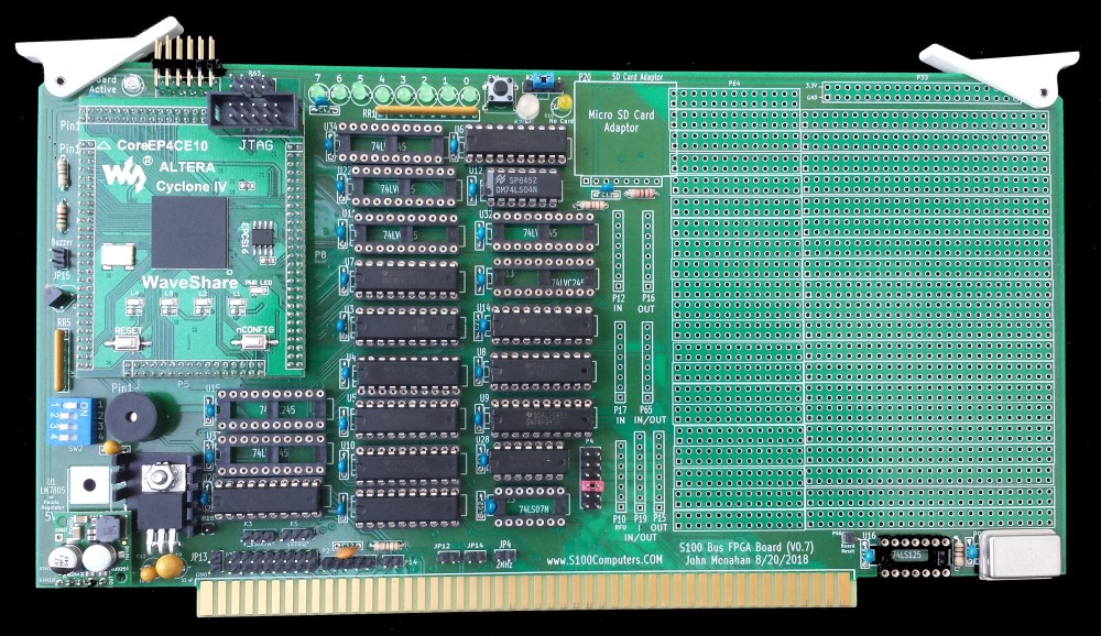
  V1.1 Final FPGA Board

Introduction
A field-programmable gate array (FPGA) is a natural extension of CPLD's and those a natural extension of the GALs we used on earlier boards.  It is in effect an integrated circuit designed to be configured by a customer or designer after manufacturing – thus the name "field-programmable". The FPGA configuration is done using a "hardware description language" (HDL).  There are two major languages Verilog and VHDL.

Verilog was created by Prabhu Goel, Phil Moorby, Chi-Lai Huang and Douglas Warmke around 1984. Originally, Verilog was only intended to describe and allow chip hardware simulation. The automated synthesis of subsets of the language to physically realizable gates etc. was developed after the language had achieved widespread usage. Verilog stands for the words "verification" and "logic". There were many upgrades/extensions over the years. The last major version appeared in 2005.

VHDL was originally developed for the U.S Department of Defense in order to document the behavior of the ASIC chips that supplier companies were including in equipment. Because of this background much of the syntax was based on the Ada programming language. The language has undergone numerous revisions and has a variety of sub-standards associated with it that augment or extend it in many ways, the last major release being in 2008.

Usage between the two tends to be polarized. Probably because of its Ada/Pascal style VHDL seems to be more popular in Europe.  The "C'" style syntax Verilog seems to be more popular in the US. 

Overlaid upon this are the chip "hardware camps".  Just like the original CPU chips, there are a number of FPGA chip manufacturers.  However there are two dominant players
Xilinx and Altera.   Recently Altera was acquired by Intel so I will refer to is as Altera/Intel.  Much of the information on the web still appears under the name Altera.   Both groups by now seem to have endless variations of their FPGA chip families.   The major ones are:-

Xilinx -- Spartan
Altera/Intel -- Cyclone.


Both companies provide extensive software to program their FPGAs.  The full blown "IDEs" are quite expensive to license but fortunately both companies now supply free "lite" versions. These lite versions are way more than adequate for our needs.

This brings me to the third component in our decision process,  picking an FPGA and programming it.   There are two fundamental ways (these days) you can program these chips. You can use the above two traditional programming languages (Verilog and VHDL) or,  you can program the FPGA using essentially a schematic and a graphic interface.  Both are available within the Xilinx or Altera/Intel IDE's .  The latter produces a special file called a
"Block Diagram File" (.bdf).  The IDE software understands this file (it actually internally makes a Verilog or VHDL file)  to program the FPGA.  The whole process is somewhat like writing a web site page.  You can either write the whole page yourself in HTML or use something like I'm using here (Expression Web),  to "draw" a web page in blocks, graphics etc.

Again, usage between the two approaches by people tends to be polarized.  The good news is that within IDE's you can import and export modules for both types.  You can for example see/export the Verilog code that makes up a complex
BDF module or you can convert a Verilog module into a BDF module.

Coming from by now, years of experience using KiCAD to lay out  over 100's of S100 bus PC boards I personally found the
BDF approach of programming an FPGA very easy. Within a day or two I was up and running programming an FPGA with quite complex circuits.   This was possible because the IDE supplies things like all the common 74xx logic chips, many of the common VSLI style chips (e.g.. UARTs),  and contains many libraries of many extremely complex/useful modules such as CPUs.  While you can drill down for detail,  at a top level they behave as "black boxes". You just supply the wire or bus connections -- which you draw as lines.   It would take me months of learning to do the equivalent in raw Verilog code.  I will illustrate this below. 

BTW, there is one well known/subscribed source code site for FPGA's called OpenCores  where you will find an enormous list of FPGA projects/code.  There numerous other excellent FPGA code applications on the web. For example Javier Valcare's FPGA home page and fpga4fun.

However first we have to decide on the hardware and software!  After a brief analysis,  I decided on the following setup:  I will work with a Altera/Intel Cyclone IV FPGA and use the Altera/Intel Quartus Prime V18.0 Liet IDE (in Windows 10).  A major factor in the choice of the Cyclone IV is that it is available as a socketed adaptor board.  The company WaveShare supplies a number of these adaptor boards.   Many of the major/recent FPGAs come only in a BGA format.   Clearly soldering chips like this is outside the capabilities of most of us. We will use their "CoreEPCE10" Cyclone IV board adaptor. Its schematic can be seen here.
    
  CoreEP4C10
    
This brings me to another "catch" with FPGAs.  While the chips can be programmed and reprogrammed indefinitely, all the information is lost when the power is turned off.   Normally you burn your program into Flash RAM which the FPGA then reads on power-up.  Few FPGAs have the Flash RAM within the chip. Most require a connection to a serial line connected Flash RAM on the actual PC board.  Fortunately the CoreEPCE10 already has this arrangement on the adaptor onboard -- in the form of a EPCS16 serial (16MB) Flash RAM chip.  This is essentially an SPI Flash device, with the physical interface consisting of the signals: MISO, MOSI, CS and CLK connected to a JTAG programming socket -- just like our CPLD chips. The Cyclone IV uses the first 256 words as a kind of  ‘boot-rom’. The rest is your own FPGA program.

One other issue using most FPGAs is the voltage(s) they require.  The Cyclone IV requires 1.2V, 2.5V and 3.3V inputs.  Normally one would have to supply 3 voltage regulators on a PC board.  The CoreEPCE10 does this from a 5V and 3.3V supply.

Finally we come to the last hurdle; With a 3.3V power supply we need a "voltage level shifters" to interface with the normal 5V 74LSxxx TTL circuits in our S100 bus.   We have seen this problem before with our Edison and Edison II boards where in that case we had to shift from 1.2V to 5 Volts.  Fortunately shifting from 3.3V to 5V is far easier. A specialized 74LVC245 chips is built for this purpose. We have however to blanket all pins on the FPGA with this chip. Any 5V input to the FPGA will irreversibly damage that chip pin and possibly the whole (expensive) FPGA.

The Board.
Broadly speaking our first FPGA board will be loosely modeled on our Edison II board.  With programming,  this FPGA board can (in theory), be configured to behave as almost any S100 bus board. Either as 1970's legacy boards or our own recent S100Computers boards. 

One thing that actually takes a bit of time to realize is how programmable these chips are. As we will see below, even with every major S100 bus pin "taken care of"  in our applications,  we have not used up even close to 1% of the FPGAs total gates capacity.   The CoreEPC10 unit has a total of 244 programmable GPIO pins.  The Cyclone IV actually has more, but they are used on the adaptor board for programming, diagnostic LEDs etc.  With that number of GPIO pins one feels like a kid in a candy store.  Unlike situations like for example the Edison CPU board,  where one has to multiplex pins,  in this case we almost always can work with dedicated I/O pins.    These pins BTW can be configured as inputs, outputs or bidirectional.   Our first "application" will be to program the board to behave as a simple port I/O board.  Later we will work up to more complete situations where the board will act as a true CPU driven bus slave or indeed a bus master.    Yes, amongst the code libraries for the Cyclone IV are very powerful CPU libraries!  There require very complex FPGA coding, but again, it's all done for us as a "black box" which one can easily utilize.

Here is a very oversimplified diagram of the board layout.
   
  Board layout

The board has a over 50 5V I/O connections at the side of the "Patch Area" that may be used for any application you might come up with. At any time one has absolute control and access to any S100 bus line. In a bus master configuration it could be in fact be the only CPU in the S100 bus.  The board also has a connector (P11) for a ribbon cable connection to a daughter S100 board with 8 direct connections (3.3V) to the FPGA.   Of course you can also add another top connector from the "patch" area to extend the boards use to a second board.

A Four layered Board
Early prototype versions of this board were 2 layered boards.  However I quickly noticed that the numerous level shifter 74LVC245s required a major portion of the boards real estate. This in effect would require a daughter board with an "Over the Top"  ribbon cable to layout any practical/functional S100 board utilizing the 50 spare pins (3.3V -> 5V) of the FPGA.  I even tried a board layout utilizing the 48 pin SMD 74ALVC164245's. These are in effect dual 74LVC245's.   That board was even worse!   In the end I decided to go with a 4 layered PC board. This frees up 1/3 of the board for any custom circuits you may design on the board.


Programming the Cyclone IV FPGA
Please keep in mind that programming an FPGA is different from the normal linear/sequential programming approach you may be used to.  On an FPGA everything is potentially happening at once.  Good FPGA programmers take years to excel and currently are in high demand.   Timing and power distributions across the chip almost become an art form.  Fortunately out needs will be far simpler.   Also there seems to be an excellent community of experienced people ready to help -- beginners.  I have found the Altera forum to be very useful and helpful.   However by far the best way to get started is to look at a few YouTube demonstrations.   

One outstanding YouTube video to get you going with Block Design File FPGA programming is this one by ClockFabrick Electronics Academy
A text summary is provided here
If you cannot get to that YouTube video you can directly view it in the video box below. However you have  to allow time for the video to upload completely (5-10 mins).
If possible use the direct YouTube link above.
Note, click on the "full screen icon" for easy viewing. Use ESC to return.   


With just that video alone you can do some serious work. 
Another pair of excellent videos are from the University of Colorado:-
Introduction to FPGA Design and Improving Productivity with IP Blocks.

Before we jump in to programming however, its nice to have a simple hardware test system to practice on. You can jump in and use the S100 board describe below directly but if you are a real beginner its nice to be able to flash a few LED's and read a few switches before you dig in deep.  At this level almost any FPGA will do.  There are many available.  I began with the Triasic DE0-Nano.
  
  DE0-nano   Wave Share Dev board Kit 
   
It's totally self contained,  all you need to do is hook it up to your PC USB port on a laptop.  I could not quickly find a simple video demo for programming a blinking LED for this board using Quartus with a BDF approach. However this one (FPGA Tutorial: Blink an LED) using Virlog directly,  is very informative to get you going. 

I should point out that one useful thing about these boards is they are very helpful at the start to test out a simple module you may be developing.   You have 4 input switches and 8 output diagnostic LED's.  As a real beginner getting the hang of FPGA programming in Quartus (even while traveling) I could test code, modules etc. easily on my laptop.   BTW, don't waste time with the Terasic software on their supplied DVD.  It does not seem to install/work correctly on Windows 10.  Typical of a Chinese company, great hardware, poor documentation/software. Just use the Quartus Prime IDE software directly.

WaveShare supplies a DVK600 kit (see the above picture), with a wide range of add-on's for FPGA program development with its Cyclone IV adaptor.  These will be very useful for developing and programming new FPGA driven S100 boards. Probably overkill for a beginner.

Quartus Prime.
The Quartus Prime IDE software package can be downloaded from this Intel site.  However you should first review this video about the installing process.  The whole Quartus Prime package is a large package, allow about 30 minutes to run the install.  If you use the Terasic development board it has its own FPGA programmer built in. Many others do also.  Most seem to utilize a "USB-Blaster" driver.    For the WaveShare unit you will need to get their USB-Blaster V2 to actually upload your code to the FPGA.  This is an excellent unit. It works simply and very relaibly from your PC USB port.

You can use the Terasic DE0-Nano to start programming an FPGA if you like.  It has 8 LEDs and 4 switches that allow you to do some sophisticated things.   However it's best you quickly get to using the WaveShare Cyclone IV FPGA.  That unit has 4 LEDs which can be programmed just by adding 5V and 3.3V power to the unit.   We will start with this.


Step By Step Building the FPGA Board
The build instructions are fairly simple for this board but because it is a complex board building it should not be rushed.  As always, first examine the bare board carefully for scratches or damaged traces, use a magnifying glass if need be.  A broken trace is almost impossible to detect by eye on a completed board.
   
Solder in all the required IC sockets, resistors, resistor arrays, capacitors, jumpers, and the Pololu 5V and 3.3V (LM3940) voltage regulators.  Do not add the LED's yet. Also do not add the MicroSD Card Adaptor. Be sure you put the resistor arrays in with the correct orientation of pin 1. Check their values before soldering (they are difficult to remove).  Insert all jumper arrays.

You may wish not to add the 6X2 double row reight angle pins of P11.  This connector has direct connections to the FPGA 3.3V pins.  Its function is to allow connection of the FPGA to a daughter S100 board board via a ribbon cable.  It's dangerous, a 5V input on these pins will severly damage the FPGA.  For any new circuit, always make sure the FPGA never sees a voltage greater than 3.3V.
 
Also note the 3 pins of K2 are for a dual colored LED not a 3 pin jumper.

If you use the Pololu 5V regulators (D24V25F5 or D24V22F5) be sure you insert them in the appropriate P1/P67 socket.   The 3.3V LM3904 3.3V regulator requires the removal of two or three of the fins on the LHS to fit under the Pololu 5V regulator. Here is a close-up picture.  Use a Jameco #70658 heat sink.  This regulator does not get even warm, but I always like to use heat sinks. 
    
    Heat Sink
Please take care to not "slobber" solder on the sockets. They are very closely spaced on this board with vias often close to a socket pin.
  
For prototype boards I generally use "double swipe" IC sockets. For a critical board like this I prefer to use "Machine Tooled" IC sockets.  However they are more expensive and you have to be particularly careful not to bend the IC pins.  The 2MHz clock oscillator can have its own special sockets (e.g. Jameco #133006) but actually I find the "Machine Tooled" IC sockets make a better connection.  I in fact solder the 2MHz oscillator (P7) directly to the board since it will never be changed.  Solder in the buzzer SP1 with the "+" pin on the RHS.
 
Place the board in the bus. There are two separate voltage rails on this board 5V and 3.3V. Carefully examine the schematic and check the voltage to the individual sockets are either 5V or 3.3V.   

BTW, your system should boot and run correctly with its Z80 master CPU board. If not, you have a serious solder bridge somewhere on the board.  Before you do anything else with a magnifying glass go over every socket on the board and examine for proper solder joints. I like to "reheat" each joint just to be on the safe side. The silk screen/varnish on these boards us quite thick. It's easy not to have a good solder joint for the ground pins.  Double check.   Extra time here will save you hours later, (Been there, done that! ). 

There is one major construction decision you need to make with this board right at the start.   The WaveShare unit uses unusual 2mm dual row pin connectors. Unlike to normal 0.1" connectors these are quite rare an expensive (Digi-Key #S5750-30-ND).  If you solder these female sockets to the board the WaveShare adaptor sits quite high on the board and will prevent the next S100 bus slot from being used.  If you carefully remove the JTAG socket top border edge with a wire cutter - all around about 1/8 "  It will fit into most S100 bus motherboards without taking up two slots. Alternatively you can solder the adaptor directly to the S100 board. Of course removing the adaptor is all but impossible in this case. 

Please note the Digi-Key #S5750-30-ND sockets for the WaveShare adaptor are quite tricky to fit on to the board.  I found the best way to do it is (after trimming to size), push them half way on to the adaptor pins and then wiggle them to fit the whole unit on to the S100 board.  Figure on spending 10 minutes on this step!  Do not solder them to the board first and then try and press the adaptor down on them. They are very fragile and internally the leaves will bend if socket angles are not exactly correct.  When in place, check each pin is visible on the back of the board before soldering.  Only then solder all around.  Add as little solder to each pin as possible - the narrow pins have a tendency to wick up solder internally. 

Leonard Young recently pointed out better sockets are available from Mouser (Preci-dip 833-87-038-10-001101)  as part 437-8338703810001101 for $3.04 ea.  You’ll need a few,  since 38 positions is a 2x19 strip.

BTW,  the KiCAD footprint for this adaptor board took me three prototype boards to get it exactly right. If you ever want to do your own board I suggest you start from this board. The large number of pins allow absolutely no margin in the fitting. 

We will first program the WaveShare/Cyclone IV FPGA just to flash the 4 LEDs on the adaptor board. For this all we need is the two above voltage regulators and the WaveShare adaptor attached to the S100 board.  Here is a picture of this setup.
     
    Step 2
    
Programming The FPGA.
Launch Quartus Prime and load the Project Demo_01.qpf and then the program
Demo_01.bdf.   All the .qpf and .bdf files we will use are supplied at the bottom of this page.  Typically you would make a folder:

C:\intelFPGA_lite\quartus\MyFPGAPrograms\S100Boards

It is very useful to have before you a printout of the FPGA board schematic and the WaveShare schematic in the steps below.  The latter for example shows the FPGA pins for the on-board LEDs. In all our programs its critical the correct FPGA pins are associated .bdf file pins.  Also make sure that Quartus Prime knows/assumes you are, (in this case), utilizing the Cyclone IV EP4CE10F17C8 chip.  Before going forward, now is a good time to take another look at the ClockFabrick Electronics Academy video.

Here is the very simple
Demo_01.bdf program.  It simply flashes the 4 LEDs on the WaveShare adaptor board. There is no interaction of the other FPGA pins with the S100 bus circuits. Note the file Demo_01.sof resides in the output_files directory. Also be sure your device is a EP4CE10F17.
     
     Demo_o1
    
If you have watched the above video,  the above
.bdf program is obvious and trivial.
Here is a picture of the relevant Programming Dialog Box.
       
    Programmer Dialog Box
   
The board only contains the 5V and 3.3V regulators and filter caps. Be sure you have 3.3V and 5V going to the appropriate pins on the Waveshare FPGA adaptor socket.
The actual compiling and programming process does take longer than you might expect (~30 seconds for the above).

Note some "virgin" Cyclone IV Adaptor boards from WaveShare have the FPGA preloaded with a program (in the
EPCS16 Flash RAM) that already pulses the 4 onboard LEDs.
Before programming the board note the rate/order at which the LEDs flash.

Upload the Demo_01.bpf  project and load the
Demo_01.brf file and program the FPGA with the Demo_01.sof file. The rate/order of the LEDs should change. 
Power down and re-power up the board. The original WaveShare rate/order of the flashing LEDs should return. 
This is because so far, for now, we are just dumping the FPGA code into the chip (not the Flash RAM).

You must get the above
Demo_01.bdf program to work before going further. Here is a picture of the programming setup.
    
    Step1
     
Once you have assured yourself that your ability to program the FPGA is sound remove the WaveShare FPGA adaptor.  Be very careful doing this. Leaver one corner at a time up a little going around and around.

Add the 10 LED's.
Before soldering them in place, and without the FPGA Adaptor, place the board in the S100 bus and ground the appropriate pins on the FPGA socket P6 to be sure they light up.    Be careful to stick a very narrow wire into pins  P6, 18-32. Also pin 18 of P7 (BOARD_ACTIVE).  Don't damage the socket pins. 

Next (carefully with a probe) jumper pin 14 of the U17 socket to 5V and orientate the dual color (3 pin) LED in K2 so it shines
Red (not Green). 
Ground pin 8 of P20 so the LED D10 lights up.
If all clear, then solder in and clip the extra wires of each LED.
(BTW, I always use a blue LED for D9 "Slave Active"  in my systems). 

Add back the FPGA Adaptor board and reprogram the FPGA with the above
Demo_01.brf program.
The D9 LED (
BOARD_ACTIVE*) should flash.

Next add U10 and U28.  Jumper P4 7-8 (XRDY). 

From your Z80 monitor display RAM
D0,FFFF

Your system should continuously scroll through your RAM display. 
With this process running, upload the
Demo_01.bdf program.
You should see the Z80 pauses and restart continuously as the S100 bus
XRDY lime pulses low.

Here is a picture of the board at this stage.  
   Step 3

While this is a very simple program it shows that your FPGA is able to control the S100 bus (via
XRDY).     This is important because you are using the U10 3.3V level shifter to activate the 5V XRDY line.

Next we will use our FPGA board to do something useful.  Again starting off very simple.   We will program the FPGA board to display on it 8 LEDs (D1-D8) the 8 bit value sent to the S100 bus I/O port
68H.  (Assuming port 68H is unused in your system. Use your Z80 Master  monitor "R" command to check)).

This will involve reading the S100 bus ports 16 address lines and the CPU's 8 bit S100 bus Data Out lines. When
sOUT goes high and pWR* goes low, the data to be displayed on the LEDs is latched.  There are numerous ways this can be programmed into the FPGA.  For simplicity,  I will use the 74xxx library approach in the .bdf file. 

The first thing one always has to consider is if the board is going to be considered a
SLAVE or MASTER bus board.  This critically defines the direction 74LVC245 level shifters to the S100 bus address, status and control lines.   We are clearly talking SLAVE mode here.  The FPGA will INPUT all these lines from the S100 bus and act accordingly.   This critical decision is set by the "DIRECTION" signal from jumper P21

LOW (Gnd)
DIRECTION = Slave Mode, S100 bus data from the bus to the FPGA.  (P21 jumpered 2-3, LED K2 Green, when U12 is inserted)
HIGH (3.3V)
DIRECTION = Master Mode, data from the FPGA to the  S100 bus.    (P21 jumpered 1-2, LED K2 Red, when U12 is inserted)

BTW, this
DIRECTION can be read on pin L16 of the FPGA if you need the information in programming the FPGA. 
For those more experienced, by jumpering K2 2-4, you can dynamically change the bus direction (
F_DIRECTION_SET, pin G16).  More on this later.

It is very important to appreciate that the boards bus level shifters (U7, U6, U5, U3, U4, U14 and U20 all 74LVC 245's) are directly connect to the S100 bus lines (on their 5V side).    These are powerful drivers.  You must always take care the their
OE* pin 19 is always HIGH unless you wish to interact with the S100 bus.   As you build your board below, always check that all their pin 19's are HIGH before adding the chip.  Fortunately all pins on the Cyclone IV are high on power up and before programming.  Carefully consider each 74LVC245s direction and OE* at all times. You do not want a bus conflict with your Z80 CPU boards buffers for example.

There are many ways a circuit could be programmed with the Cyclone IV and this board to write to an S100 I/O port.  Rather than be smart/elegant I will use a simple brute force approach.    This is one of the things you quickly realize using FPGA's is that there is almost endless supply of gates.  It is doubtful you will ever get close to using up the chips programming capacity, so you can afford to be "sloppy" duplicating circuits, overkilling "what if" scenarios etc.  You will find yourself laying down circuits that you would never consider on a 5"X10" S100 board with 74LSxx chips.  That said,  I cannot over-emphasize the importance of adding functionality one step/circuit at a time as you build your circuit.  Use the four onboard LEDs (L1-L4) of the WebShare adaptor board to flag/indicate your process.    Finally, I recommend you save your
.brf file (as a different name) as you step things along. That way if all fails, you can fall back to a previous version.  (Saved my neck several times already).

Quartus Prime is very powerful with almost endless options.  I do find it's somewhat "finicky" however with cut and past of circuits in your
.brf file.  Its best to add circuits from the top menus as you need them. 
 
Add U12 and jumper P21 2-3 (
Slave Mode). 
Add U7, U6, U5, U4, U9, U14, U20 and U17.  Place the card in the bus and check pins 1 & 19 of each chip is HIGH.  The LED K2 should be
Green.
U17 pin 19 will always be low and its pin 1 high.

Open the Project FPGA_Board_Port_Output_Test.qpf and the file
FPGA_Board_Port_Output_Test.bdf from the bottom of this page. 
If you have built any of our many S100 Bus boards in the past you will have no difficulty understanding the FPGA "circuit". 
Essentially the FPGA reads the bus address lines
A0-A15 and sends them to a pair of 74684 comparators.  If it detects a bus output (sOUT high) for port 68H it will send the eight S100 bus Data Out lines to internal latches which are read by the eight onboard LED's.
Here is the core
.bdf circuit.
Using our Z80 CPU board and its Master monitor to output to port
68H should set the LEDs. For example:-
 
QO68,33

     
   PortOut2
 
As you can see the circuit is dirt simple. In writing programs/circuits like this you do have to be very careful that you assign the correct FPGA pin number to each signal. 
As mentioned above, always be careful with the 74LVC245
OE* pins.

Next will write a simple FPGA program to allow our Z80 to read a value from port 68H.
Add U3 & U8.  Again check their pins 1 & 19. 
We will use the onboard 4 position dip switch
SW2 to define the upper and lower nibbles of the port data. 
This time open the Project FPGA_Board_Port_Input_Test.qpf and the file
FPGA_Board_Port_Input_Test.bdf.  The circuit is essentially the same as the previous one except this time we use the Z80 master monitor to input a value from port 68H.

QI68, 00110011

The core circuit is shown here.
    
  PortIn1

You should always see the 4 bit value from SW2 in the upper and lower nibbles from your Z80 master monitor. If not don't go further until you resolve the problem.  For example enter the following Z80 code in RAM at 0H and jump to it.

DB 68
C3 00 00


Add LED "flags" (L1,L2,L3 or L4 on the FPGA Adaptor) at various points in the .bdf to see where the problem is for debugging.
Here is a picture of the board at this stage.
  
    Step 4
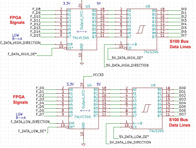
This brings me to the next item on this board.  As I have already explained above, all the 74LVC245 level shifters directly interface with the S100 bus.  I situations where the board is in a Slave configuration bus loading should not be an issue. Even in a 22 slot S100 bus, standard 74LS244/245 type buffers on other boards should have no problem interfacing with this board.  Indeed even in master mode,  the U5, U6, U7, U14 and U20 74LVC245s  (in my 22 slot system)  seem to work fine driving the S100 bus address, status and control lines.  I was however worried about the S100 bus data lines (the eight DI and DO lines).  To be safe,  I have spliced in a standard 74LS245 between the U3 and U4 74LVC245 and the S100 bus.  The direction and OE* pins of these two buffers should track/behave exactly the same for both the 74LVC245s and 74LS245s.  I'm not absolutely convinced both buffers are necessary -- almost definitely not for small S100 systems, but its nice to overkill on these critical S100 bus data lines. They fan-out to almost every board in the bus.  Here is the circuit on the board.
 
      Data Buffers

Now let us combine the two circuits. We will have an output port and input port at
68H.  The circuit is essentially a combination of the two above circuits with some bells and whistles.  Load the Project Port_IO_Test.qpf and the file Port_IO_Test.bdf and program the FPGA.
In this mode when you output to port
68H in your Z80 monitor you should see the LED's display the correct Hex value.
When you input from port
68H you should get the same value back.

QO68,33
QI68
00110011


The FPGA Board as a Bus Master
Now lets move things up a notch in terms of complexity, lets configure the board to temporary
Master mode and have it control the S100 bus lines rather than reading them.  We will have the board act as a Temporary bus master (just like our many previous CPU boards such as our 8086, 80486, 68030 etc.).   Note this configuration is not for everybody.  Switching S100 bus control is tricky (see here), the vast majority of applications for this board will probably be as a bus slave. Nevertheless since the Cyclone IV has its very own internal CPU (called Nios II), a bus master role is interesting.

First we jumper P21 1-2 so
DIRECTION is HIGH (3.3V). The LED K2 should now be Red.  This way the 74LVC245 buffers U7, U5, U3,U4, U14 and U20 are outputting to the S100 bus.  Critically however, in every case the OE* pin is High.  (All FPGA pins are high on power-up). 

Add U11 and U16. Jumper P4 1-2 and P2 4-5. Add jumper JP15 for the buzzer.  Jumper P2, 4-5 (TMA0*).

Next just as for our many other CPU boards,  we need a circuit to transfer control from the Z80 CPU board (the Bus master) to our new Temporary Bus Master on the S100 bus.  This process is explained in some detail here.  After reading that article the FPGA_Board_AddressLinesTest.qpf project and
FPGA_Board_AddressLinesTest.bdf file (see the bottom of this page), should make sense. Here is the key Master/Slave transfer circuit.  For simplicity we will generate a PHI clock of 1MHz.  (By changing the Clock PLL01_50 it can be anything up to about 10MHz).
   
    Handshake

The two above signals XFERI and XFERII are then utilized in the sequential transfer of control of the Z80 Address, data, status and control lines to the FPGA board.
The SMB actually requires a valid pSYNC, pSTVAL and pDBIN to latch the address lines into that boards HEX digital display. These are synthesized by the circuit below.
      
    Control Signals
  
To run this "program", boot up your Z80 and load up the FPGA code. Then transfer control to
TMA0 from your Z80 Monitor ("O"  command).  You should see the S100 bus Address lines and Data lines continuously change in value.  Here is a short video.


Here is a picture of the board at this stage:-  
   Step 5
Pressing the SW1 switch will hold the address & data lines. The buzzer should also sound.  Releasing the SW1 button and the count process should continue.
Please study and understand everything in the FPGA_Board_AddressLinesTest.bdf file before proceeding further.  It is essential that you understand ever aspect of that file before going further. From now on almost everything is going to be FPGA programming! 

Add all remaining IC's to the board. We will utilize the almost 60 spare pins of the Cyclone IV to adapt the board to our own custom circuits or old S100 Bus Board emulations.

Future FPGA Code/Configurations will be listed below.

Burning FPGA Code to Flash RAM.
Up until now whenever we programmed our FPGA via  the JTAG socket the data is lost whenever the power is turned off.   While fine for code development etc. it is not desirable for a final board configuration.  Like most FPGA applications the "final" code is saved in Flash RAM and immediately loaded by the FPGA each time upon power-up.  This is a standard and common characteristic of most FPGA's. Some older models in fact had a ROM onboard.    Our Cyclone IV Adaptor board has 16MB of Flash RAM on board for this purpose -- way more than we are ever going to need!

The tricky part is programming this Flash RAM.  I found the Intel documentation poor and confusing.  Here is a summary of the process: 
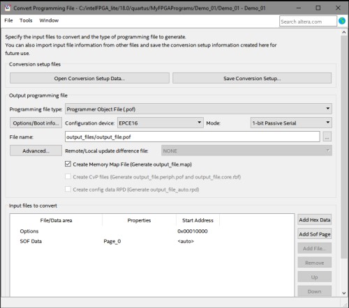
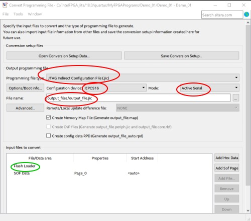
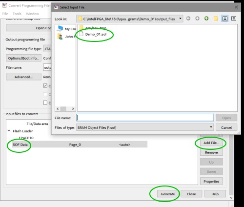
Within Quartus you need to "convert" your normal JTAG FPGA
.sof programming file to a special file .jic to program the Serial Flash RAM chip on the Weveshare board.

Within Quartus, click on the File Menu and select "
Convert Programming files". The dialog box below will popup.
From the dropdown box on the "
Programming File Type"  select a .jic file type.
This is the file format that is required to program the onboard serial Flash RAM.
For the
Options/Boot info select EPCS16. Leave Active Serial as is.
You can name the
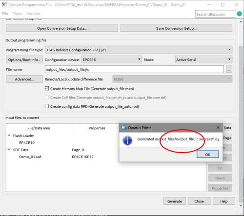
.jic output file anything you like. I usually just leave it output_file.jic.
Note it will be in the Ouartus generated "output_files" folder within your work directory.

Next click on
Flash loader within the lower "Input Files to Convert", then click on the highlighted "Add Device" button.
You will get a popup dialog box as shown below.
Select
Cyclone IV  and EP4CE10.  Note Quartus takes some time to allow you to actully select these options -- seems to be doing things in the background!
Next click on "
SOF Data" and "Add File".  You should see your "normal" FPGA program .sof file in your "output_files" folder within your work directory.
Finally click the "
Generate" button.
You should get a popup dialog saying "Generated
output_files/output_file.jic successfully.
Note the name and location of the converted file. Then close that dialog box.  See the pictures below.
                
    Programming 1     Programming 2
 
Programming 3 Programming 4
   
Programming 5
  
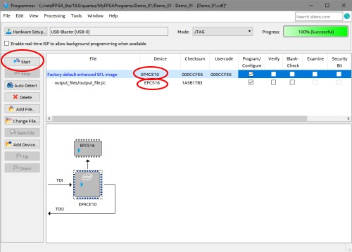
Next we need to actually flash the Waveshare boards RAM chip.
Click on the normal "Progarm Device (Open Programmer)" you normally use. If its not already open,  give it time to come up as a dialog box.
Make sure your board has power.  To be safe click the Auto Detect button. your normal xxx
.sof file should display with the device set as EP4CE10F17.

First delete the above line
xxx.sof  |  EP4CE10F17 etc.
Click on
Add File and select the xxx.jic file (in your file_output directory) you generated above.
Click on the Program/Configure little square character.
The
Start button should highlight.
Click on this and you will flash the RAM chip.  Follow the Progress bar until it is done.
You can power off and re-power your computer.
Your FPGA board should (after reset), start with whatever FPGA code is within the chip.
 
Programming 8
 
Note when you close the above dialog box, normally you do NOT save the changes.
Typically you want the chip to be quickly reprogrammable.


FPGA Code & Board Circuits.
This section, over time, will contain seperate page links on this site to new FPGA code and board circuits using the above board. There are now almost limetless examples of FPGA code in the public domain for most major digital electronic circuits. Three popular sites are OpenCores, Grants MUlTICOMP and fpga4fun. If you develope a usefull FPGA application with this board please consider sending it to me, I will place it in this section.

      Board Circuit Name  (Click to Select)          Board Description  
  UART_PORT   A simple UART port interface to the S100 Bus.  
    1602 LCD Display    Interfacing to a dual line 1602 LCD Display Module 
    A VGA PONG GAME   A simple VGA interface demo. 
    RAM_DEMO    A 4K OnChip Static RAM Circuit 
    PS2_KEY    A simple PS2 keyboard input port example 
    PS2_LCD    Display a PS2 keyboard input on a 1602 LCD Display 
    SPI INTERFACE    An SPI 16 bit Communications Interface to a Digital Potentiometer
    I2C INTERFACE    An I2C Communications Interface to an EEPROM
    SPI_INTERFACE V2    An improved SPI interface with 8, 16, 24, 32, 40 or 48 bits 

Installing Quartus Lite on Windows.
In spite of its name the
Quartus Lite IDE is a large program.  When fully installed the Quartus folder is over 15GB in size.  Installing it makes Microsoft's Visual Studio seem lightening fast! 
 
That said,  its an excellent IDE.  Figure on 1 hour to install and get it right.  For our purposes we will only be using probably 5% of its capabilities, but I have found if you try and get smart by not downloading or removing sections you run into problems later during usage. 

Please see here for instructions on how to install Quartus.

Quartus Prime Tricks & Shortcuts.
The Quartus Prime IDE software package is very extensive.  There are numerous configuration options. Even simple things like changing the menu icons choices can be frustrating. Unlike for example Microsoft's Visual Studio etc. you cannot drag and drop them -- at least in the current version.    If you try and get too smart editing/copying images in the .bdf window the program can get confused.  A few things I learned the hard way...

1. Be very careful when you place multiple copies of a logic item. Sometimes when you click you can place one item exactly over another yet the item appears as only one unit. For example a
NOTor a NOR gate. The compiler will insist the gate has no input when in fact the hidden gate under it is the problem.

2. Be careful when you join up and input or output port to a wire or bus line. Make sure they join by dragging them apart.

3. Some gates are negative true. I use names like pWR- to signify this. Quartus does not accept pWR*.

4. As I said above build a circuit in stages of increasing complexity saving versions along the way.

5. Be sure the designated FPGA for a new project is a
EP4CE10F17C8 for the above WebShare board.

6. Quartus is built with a large project in mind. It's not really well suited for multiple small projects like we have here.  I like to have each project in its own Windows directory.  When you create a new project this way you start with a clean blank page.  It's a real pain to have to each time lay down the basic S100 bus interface and pin designations.  While the may be a short cut I have not discovered I found the easiest way to do this is to do the following:-
 
            Create a new project say
NewProject.
            Create a new
.bdf file (NewProject.bdf).
            Add one item to the
NewProject.bdf file, say a NAND gate.
            Close the complete project.
            Then copy a previous S100 bus "
OldProject.bdf" file into the above directory.
            Delete the above
NewProject.bdf file and rename the OldProject.bdf file to NewProject.bdf.

Now when you launch the
NewProject.qpf and load the file NewProject.bdf you will have window from which you can add or remove items.

There is only one catch.  The pin designations did not come across.  On complex circuits these are a pain to add each time.  This is where it gets a little messy!
Pin info is in a
.qsf file.  If you bring the OldProject.qsf file across and rename it to NewProject.qsf  Quartus gets confused.  Here is what I found works:-
 
           Open
NewProject.qsf in Notepad and go to the very end of the file.
           Also open
OldProject.qsf and copy only the lines that start with set_location_assignment PIN.... to the end of the NewProject.qsf file
           Close both files.

Now your
NewProject.bpf project has pin designations and is ready for development.
Remember also in most cases you will have to bring across the library files (e.g. the
PLL01.* and Counter01.* files).

7. FPGAs only work with digital logic. So any circuit that requires a resistor or capicitor will have to be emulated in other ways. For example there are no 74121 or 74123 "chip" libary .bdf files. You could implement them using FPGA I/O pins but its far easier to use digital counters etc. Also for most FPGA chips, Open Collector gates are not available.  This requires you to emulate OC outputs to I/O circuits for example with OR circuits etc.

8. I have found if you sometimes take shortcuts in saving files under a different name/directory to later use it as a starting point for another project that Quartus can get confised and actully work on a different file by the same name.  When starting a new project using an old project (copied from a different directory) as a starting point I always delete the previous Quartus generated directories "
db", "incremental_db" and "output_files" in the new directory.  Quartus will regenarate them with a clean slate.

9. When you use the “Program Device” dialog box to actually burn the FPGA be sure the .sof  is the actual source file for the new burn. If you setup the Quartus source code folder is a different directory than when the original file was made the “output_files” path will be different. You need to delete the old path and “Add File” to a new one.  Quartus does not show the complete path.  

For more information about installing Quartus see here.

Bugs
1.    The silkscreen for the Q1 transistor is wrong. The flat side of the PN2907A transistor should be towards the side of the board.  The actual pins are correct. The bottom pin, the collector, is connected to the SP1 buzzer.
2.    Some of the pins coming from the Waveshare sockets actually go to more than one 74VCL245.  I don’t know how that happened.  At one point I must have been thinking bidirectional I/O or something.  Most of the “bad pins” are on P5:-  1,3,5,7,9,11,13,15.  Not a problem if you watch the directions of the buffers. Will be corrected on V2.
3.     There appears to be a few variations of the 74LVC245 20 pin DIP level Shifters chips with "A", "AN" etc after the 245.   As best I can tell so long as they are 20 pin DIPs they are all OK. I use Mouser chips # 595-SN74LVC245AN.

A Production S-100 Board

Realizing that a number of people might want to utilize a board like this together with a group of people on the  Google Groups S100Computers Forum, a "group purchases" is now open. Contact and join the group if you would like to be involved in this project.  Please see here for more information.
 
Please note the final verson of this board (V1.1) differs very slightly from some of the pictures on this page.  (The most significant difference is the addition or the 1K rersistor network RR2). The build and testing process remains unchanged.

The links below will contain the most recent schematic of this board.
Note, it may change over time and some IC part or pin numbers may not correlate exactly with the text in the article above.


Most current KiCAD files for this board         (V1.1a  Prototype zip  files  10/12/2018)
Most current Gerber files for this board       (V1.1 Prototype zip  files  10/3/2018)
Most current Schematic for this board         (V1.1a Prototype zip  files  10/12/2018)
Parts layout this board                               (V1.1a Supplied by Rick Bromagem  10/13/2018)
BOM for board (XLS File)                          (V1.1a Supplied by Rick Bromagem  10/13/2018)
BOM for board (.PDF File)                       (V1.1a Supplied by Rick Bromagem  10/13/2018)


Demo_01.zip    (V1.0  9/5/2018)
PortInTest.zip    (V1.0  9/5/2018)
PortOutTest.zip   (V1.0  9/5/2018)
Port_IO_Test.zip     (V1.0  9/5/2018)
AddressLinesTest.zip  
 (V1.0  9/5/2018)

Other pages describing my S-100 hardware and software.
Please click here to continue...

This page was last modified on 10/19/2022