An FPGA RAM Demo Circuit.
This
circuit example adds 4K of static RAM to our FPGA Prototype board.
When this RAM is addresses (currently at 8000H-8FFFH) in the S100 bus the S100
Bus Phantom line will be
assessed thereby inactivating any other RAM in the
system at that location. Note no hardware changes are made to the FPGA
board itself. All the circuits reside within the FPGA chip.
Introduction.
Most recent FPGA chips have the capability to be programmed to contain static
RAM. The Cyclone IV can contain up to 4K of static RAM (8 bits wide).
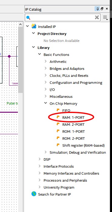
If you look at the Quartus IP window you will see that Intel supplies a few
different types of static RAM already packaged for us.
We will use the simplest type here, RAM with a single access buffer.
Clicking on it brings up a 5 step dialog box. Interestingly, you
will see that the RAM can be up to 256 bits wide. We will use 8 here. Also the
amount of RAM can be up to 16K -- though I'm not sure of these parameters for
the Cyclone IV.
A detailed description of all the FPGA Cyclone RAM (and ROM) options is
described in this Intel document.
Writing to, or reading from, this On Chip RAM is very simple -- along the lines
you would layout a "real" RAM board circuit. Again for speed and
simplicity we will use the Quartus .bdf file approach. So when you are
setting up the RAM parameters in the above dialog box at the last step, you save
the file as a .bdf file. Your new RAM dialog will then appeared as an
option in the Symbol/Project dialog on the toolbar. I named it
ON_CHIP_RAM2 in this
example
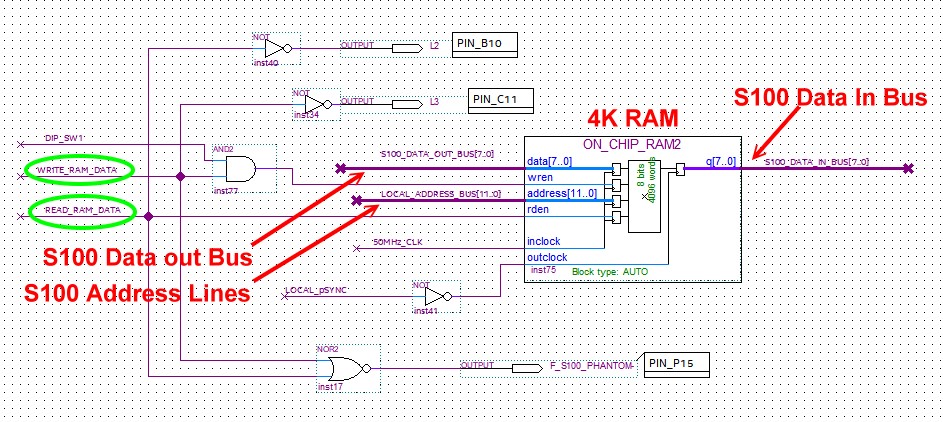
Here is the core of the FPGA circuit:-
The two key signals coming into the RAM circuit are
WRITE_RAM_DATA and
READ_RAM_DATA.
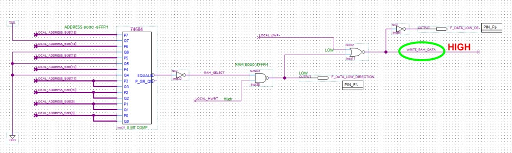
Again a very simple circuit. When the equivalent of the 74LS684 sees an
address range between 8000H and 8FFFH it goes low. Any Memory write will raise
the WRITE_RAM_DATA signal. A similar circuit is used for
READ_RAM_DATA.
The data is only written to, or read from the RAM, when these signals are high.
Any other address line changes are ignored. The above Intel IP
Library actually latches the data with a Low to High clock signal.
pSYNC (inverted) seems to
work file for RAM reads. I could not get a common S100 bus signal to work
for inclock. Fortunately it does not seem to be critical, any fast
clock seems to do. I used the 50mHz FPGA clock.
A few things of note in the circuit:
1. You will see i am reading and writing to the S100 bus data in and
out lines directly. The is no need for an extra layer of buffers. Of
course the FPGA pins are not directly connected to the S100 bus, the still go
through the level shifters/drivers U3+U8 and U4+U9. Thus we need
F_DATA_LOW_OE-, F_DATA_LOW_DIRECTION etc..
2. Since most systems these days will have 64K of static RAM you
don't want a memory conflict. The S100 bus has a special line "Phantom"
(Pin 67) which if low can inactivate a RAM board in the system.
Be sure to jumper P4 3-4 with a short wire bridge. We
use the FPGA pin F_S100_PHANTOM
to do this in our circuit. When low, the only active RAM is from the FPGA board.
3. You will notice that the
WRITE_RAM_DATA signal requires the dip switch SW1
to be high to be active. If it is low the ON_CHIP_RAM2 circuit behaves as
a ROM. In other words you can read the data but not (over) write it.
Testing.
The easiest test of RAM like this is to move your Z80 monitor at F000H-FFFFH to
8000H and jump to 8000H.
MF000,FFFF,8000
G8000
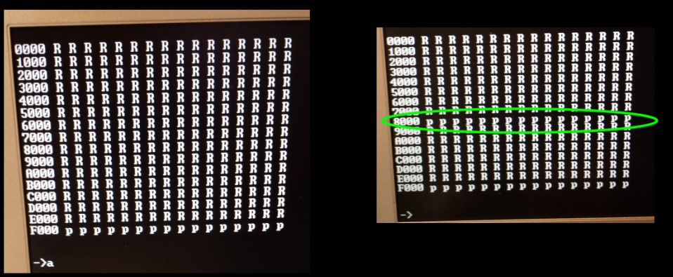
The Master Z80 monitor (at 10Mhz) should still sign on and run.
If you do a "A" command you should see RAM from 0H to EFFFH. If you set
the dip switch low you should see "P's" at 8000H to 8FFFH, but the monitor
should still run.
Here are two pictures:-
If this works you have a solid and reliable RAM window on your
FPAG prototype board.
RAM_DEMO.ZIP
RAM_ROM_INFO.PDF
This page was last modified on
05/11/2019