S100 Computers

Home S-100 Boards History New Boards Software Boards For Sale
Forum Other Web Sites News Index    
 
The S-100 BUS Pin Designations and Board Layout 
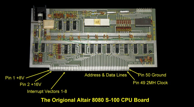
The original S-100 board bus interface pins were laid out (in a hurry) by an unknown engineer who worked as a contractor for MITS.  Unfortunately the pin arrangement is somewhat hap-hazard and not the best for noise resistance either. The exact pin placement/function on either side of the board was simply determined by the easiest way to bring all the 8080 pin signals down to the bus with a minimum of plated through holes on the board.  This was done before the days of the efficient CAD/CAM PC board layout programs we have today.   If you look at this 8080 board, there are remarkably few plated through holes on the board.  Fortunately MITS had the foresight to include S-100 bus vector interrupt and a DMA request line even though they were not used in those early systems.  Here is a picture of a very early MITS 8080 CPU board:-
The Origional 8080 MITS CPU Board

 
The following is a list of the pins of the S-100 bus as describe in the IEEE-696 specification along with some comments.
The original draft submitted to the IEEE can be obtained here.
The final version can be obtained here.

1  + 8 Volts     The instantaneous minimum must be greater than 7 volts. The average maximum must be less than +11 volts and the  instantaneous maximum must be less than 25 volts.  The optimum voltage is 8 Volts,  but many drop the voltage to 7.5 volts to lower heating of on-board voltage regulators.
  
2 +16 Volts The instantaneous minimum must be greater than 14.5 volts. The average maximum must be less than +21.5 volts and the  instantaneous maximum must be less than 35 volts.  The optimum voltage is 16 Volts.
  
3 XRDY This is a signal that is asserted by a slave to tell the master that it is ready to complete the current bus cycle. The slave may drive XRDY low to tell the master that it is not ready to  complete the operation. This will cause the master to wait until RDY goes high again, in effect extending the current bus cycle.
   
4-11 VI0*-VI7* There are 8 interrupt lines on the bus. A low on any one will signal to the current CPU that and interrupt is required. They are typically assigned priorities by an interrupt controller chip.
   
12 NMI* A low on this line triggers an immediate NMI interrupt. This signal need not generate an interrupt acknowledge and is edge triggered. On a Z80 if INT's are enabled the CPU will jump immediately to memory location 66H.
  
13 PWRFAIL* Seldom actually implemented but triggered to warn the CPU/system on a pending power loss.
  
14 DMA 3* One of 4 lines a temporary bus master sends to the bus Master bus controller signaling that it wants to have control of the bus. Examples would be an 8086  taking control of the bus from a Z80 bus master or a disk controller temporarily using the bus for direct memory access. 
 
15 A18   
16 A16    
17 A17
 
18 SDSB* When this line is low the status lines sMEMR, sWO, sM1, sINP, sOUT, sHLTA and sXTRQ normally controlled by the permanent bus master are floated. This allows the temporary master to control these lines.
  
19 CDSB* When this line is low the status lines pSYNC, pSTVAL, pDBIN, pWR and pHLDA normally controlled by the permanent bus master are floated. This allows the temporary master to control these lines. Note MWRT is not affected by CDSB.
   
20 GND On old systems this line was controlled from a front panel to stop or allow writing to RAM. Was almost never used. Now dedicated to a badly needed ground line in the center of the board.
  
21 NDEF This was the old S-100 Single Step line. It was generated by the front panel. Single step hardware is useful for debugging but there is no need for this line.  CompuPro (and possibly others) used this line in some boards (for example their 68000 CPU board) as a Master Clock disable to allow slaves to come on the bus with a different clock speed.
 
22 ADSB* When this line is low all address lines (A0-A23) normally controlled by the permanent bus master are floated. This allows the temporary master to control these lines.
  
23 DODSB* When this line is low the data output lines (DO0-D07) normally controlled by the permanent bus master are floated. This allows the temporary master to control these lines.
 
24 PHI This is the main system clock for the bus from which all other signals are linked. Both the master and slave CPU's use this signal. The bus specs are unclear as to how to implement a faster clock for a slave CPU.
 
25 pSTVAL* A very important signal. This strobe indicates the information on the bus for the address and status lines are valid. Note it is only meaningful when it occurs with pSYNC.
 
26 pHLDA This is a signal that indicates that the master has relinquished control of the S-100 Bus to another master.
 
27 RFU Not currently utilized.  Some people use it as a line for inverse master Clock (24). This allows boards like the Versafloppy II to work that count on the old Clock 1 signal on pin 2
 
28 RFU This was the old PINTE line. It monitored the 8080 to show when INT's are enabled. The signal was never used
 
29 A5  
30 A4  
31 A3  
32 A15  
33 A12  
34 A9
 
35 D01/DATA 1 Data bit 1 out to the bus for an 8 bit CPU, bidirectional data bit 1 for 16 bit data
36 DO0/DATA 0 Data bit 2 out to the bus for an 8 bit CPU, bidirectional data bit 1 for 16 bit data
 
37 A10
 
38 DO4/DATA 4  
39 DO5/DATA 5  
40 DO6/DATA 6  
41 DI2/DATA 10  
42 DI3/DATA 11  
43 DI7/DATA 15
 
44 sM1 The name M1 comes from the old 8080 designation for an op-code fetch cycle. This status line signifies that the master is fetching an instruction from the bus. Depending on the implementation of a particular master, this line may also be active during an interrupt acknowledge cycle.
 
45 sOUT This status line is active when the master is executing an output cycle and writing data to an I/O port address.
 
46 sINP This status line is active when the master is executing an input cycle and reading data from an I/O port address.
 
47 sMEMR This status line is active when the master is reading from a memory adders. It will go high for all memory reads including  an op-code fetch.
 
48 sHLTA This status line is active when the master enters a Halt state. An 8080, 8085, or Z80 microprocessor enters the Halt state by executing a HALT instruction. An interrupt request or reset is the only way to get out of a halted state, so this instruction is usually used to wait for an interrupt to occur. This instruction may have no equivalent in other processors. In that case, the processor would never enter the Halt state, and therefore sHLTA would never become active.
 
49 CLOCK  This is a 2 MHz clock signal that does not have to be synchronous with the system clock.  The frequency tolerance is + or - 0.5% and the duty cycle is between 40% and 60%. This signal is used as a timing reference for baud rate generators, real-time clocks, and interval timers.
 
50 GND  
     
     
51 +8 Volts The instantaneous minimum must be greater than 7 volts. The average maximum must be less than +11 volts and the  instantaneous maximum must be less than 25 volts.  The optimum voltage is 8 Volts,  but many drop the voltage to 7.5 volts to lower heating of on-board voltage regulators.
  
52 -16 Volts The instantaneous minimum must be less than -14.5 volts. The average maximum must be grater than -21.5 volts and the  instantaneous maximum must be grater than -35 volts.  The optimum voltage is -16 Volts.
  
53 GND This was the old S-100 bus Sense Switch Disable. It was used to active a circuit on the front panel to input data directly from panel switch.
 
54 SLAVE CLR* This signal resets all bus slaves to a known condition. Note that SLAVE CLR* used to be called EXT CLR*, for external clear. The function is still the same, but the name was changed to be consistent with the terminology of the standard.
 
55 DMA 0* One of 4 lines a temporary bus master sends to the bus Master bus controller signaling that it wants to have control of the bus. Examples would be an 8086  taking control of the bus from a Z80 bus master or a disk controller temporarily using the bus for direct memory access. Note: The old Victor Graphic 48K Dynamic RAM boards used this line to present a short reset signal on the bus to insure the Z80 could refresh RAM correctly. See here
 
56 DMA 1*  
57 DMA 2*
 
58 sXTRQ* This is a new status line that is asserted by the master to request that a 16-bit data transfer occur during the current bus cycle. If this line is not asserted (if high) then an 8-bit transfer will be requested by default.
 
59 A19
 
60 SIXTN* This signal is asserted by a slave device if it is capable of a 16-bit data transfer. If the master asserts sXTRQ* and SIXTN* is asserted by the addressed slave within a short  period of time, then the master may proceed with a 16-bit data transfer. If SIXTN* is not asserted by the slave, then the master should perform the transfer as two 8-bit transfers. If the master is not capable of performing the 16-bit transfer as two 8-bit transfers, an error condition will result immediately, with ERROR* asserted.  SIXTN* is a new S-100 signal not fount on old S-100 boards. However it has been implemented in a way that makes it compatible with these S-100 boards - an 8-bit memory board would never assert SIXTN*.
 
61 A20  
62 A21  
63 A22  
64 A23
 
65 NDEF
 
66 NDEF Some boards use this line for an output signal from the Z80 refresh signal (for example Vector Graphic's Z80 board).  When low, the lower 7 bits of the address lines hold the refresh address for dynamic RAM boards.
 
67 PHANTOM* This signal is provided so that slave devices may exist in the same address space by overlaying one another. One device (the phantom device) is inactive if PHANTOM* is inactive and a normal device is active. When PHANTOM* is asserted, the phantom device becomes active and the normal device becomes inactive. PHANTOM* may originate anywhere on the bus.
 
68 MWRT This is a memory write strobe that is not disabled along with the other control output bus signals. MWRT is derived from the following equation: MWRT = pWR-sOUT. In other words, when pWR# is true and sOUT is false, a memory write cycle is occurring.  Note MWRT be generated by only one device in any system. It may originate on the permanent master, a front panel, or on any other device that is permanently in the system. MWRT should be generated by the actual bus signals pWR# and sOUT. This ensures that any master will be able to write into memory which uses MWRT.
 
69 RFU
 
70 GND This was the old S-100 bus PS line. I was connected to the front panel LED to indicate that memory was protected from writing.
 
71 RFU This was the old S-100 RUN signal. It was high when the CPU was running and low when the front panel had stopped the machine. It was never widely used.
 
72 RDY RDY is a signal that is asserted by a slave to tell the master that it is ready to complete the  current bus cycle. The slave may drive RDY low to tell the master that it is not ready to complete the operation. This will cause the master to wait until RDY goes high again, in effect extending the current bus cycle.
 
73 INT* This is the general purpose interrupt request line for the S-100 Bus. It is usually maskable by a software instruction. When asserted by a slave, assuming the master has not masked interrupts, after completing the current cycle the master will enter an interrupt acknowledge cycle or cycles. Usually the interrupting device will send some kind of information to the master during the interrupt acknowledge cycle.  Note that INT* should be asserted as a level, meaning that INT* should remain low until the interrupting device has been serviced.
 
74 HOLD*  This signal is asserted by a temporary master to request that the permanent master relinquish the bus to the temporary master. The temporary master should continue to assert HOLD# until it determines that it is either done with the bus or will not be granted access. HOLD* may be masked at any time by the permanent master.
 
75 RESET* This signal resets all bus masters to a known condition. Any bus slave that needs to start in a known condition relative to the master may also be reset by RESET*. RESET* is often connected to a pushbutton switch located somewhere on the machine.  Note some of the early dynamic RAM boards (that did not have their own onboard refresh controller and relies on the Z80 refresh signal) suffered data loss if the refresh pulse was too long.
 
76 pSYNC This is a strobe that indicates the start of every bus cycle. It becomes active very near the beginning of every bus cycle, and remains active for approximately one cycle of the bus clock (pin 24).
 
77 pWR*   This signal is the generalized write strobe for the S-100 Bus. It is asserted for memory and I/O write cycles. It is used by the slave device to tell when the data output bus contains valid data.
 
78 pDBIN   This signal is the generalized read strobe for the S-100 Bus. It is asserted for memory read, I/O read, and interrupt acknowledge cycles. It is used by a slave device to turn on its data  bus drivers so that the data to be read is gated onto the bus at the proper time. The master should sample the data near the end of this read strobe.
 
79 A0  
80 A1  
81 A2  
82 A6  
83 A7  
84 A8  
85 A13  
86 A14  
87 A11  
88 DO2/DATA 2  
89 DO3/DATA 3  
90 DO7/DATA 7  
91 DI4/DATA 4  
92 DI5/DATA 13  
93 DI6/DATA 14  
94 DI1/DATA 9  
95 DI0/DATA 8
 
96 sINTA This status line is active when the master is responding to an interrupt request and expects the interrupting device or interrupt controller to place data on the Dl bus during this cycle.
 
97 sWO* This status line is active when the master is currently executing a memory write or an output write cycle.
 
98 ERROR* This is a generalized error signal line that can be used to inform the master that some kind of error has occurred. This can be a memory parity error, an attempt to write into a protected memory location, an attempt to perform a 16-bit transfer to an 8-bit device, etc.  This feature was rarely  implemented on the bus. On the Altair S-100 bus, this line was used to monitor the 8080 Stack line status. No other CPU have such a signal. Was never used. SD Systems on early boards, used this pin as a "debug" line. When forced low their CPU board forced address lines A14 & A15 low allowing their monitor program to go to address C000H.  Some even older boards used pin 98 as a dynamic RAM refresh signal.
 
99 POC* This signal must start out low when the system powers up, and remain low for at least 10 milliseconds after power is stable. POC* must be active only at power-on. POC* must also assert RESET* and SLAVE CLR*.
 
100 GND   Ground

TMA and S100 Bus Temporary Masters.
When microprocessor CPU's first came out they were not particularly fast -- often with a clock speed of only 1-4MHz. When a fast process was required -- for example a video application - a direct memory access "DMA" approach was often taken.  Another chip or circuit would stop the CPU take control of RAM and carry out the function, returning control back to the CPU when done.  This could be brief for example a video RAM read as in the case of the Cromemco TV Dazzler or longer as for example for many FDC boards.  In these applications DMA was a very efficient process.  However as more and more S100 boards appeared from differing manufactures timing issues started to arise. There was no agreed upon standard of "handshake" process between the CPU and the "DMA Controller".

As the IEEE S100 bus working group of Mark Garetz, George Morrow, Howard Fullmer and others began formulating a standard for the S100 bus David Gustavson proposed a scheme that would allow up to 16 DMA devices to exist on the S100 bus.  Over time this evolved into the concept of up to 16 controllers in a rank priority scheme being allowed to run the bus.  The actual priority each potential controller had could be defined in hardware by the bit pattern of 4 unused (at that time), S100 bus lines later named TMA0, TMA1, TMA2 & TMA3.  They would be known as "Temporary Masters" or "Slave Controllers". They only obtained control of the bus when allowed to do so by the "Bus Master".  The latter usually being a Z80 CPU. This combined with the 8 or 16 bit data paths of the S100 bus allowed for an dramatic increase in its utility.  Let us look at the process of how this transfer of control from the S100 bus master to a Temporary master/Slave actually is implemented. First in theory, and later in practice by S100 board manufacturers.

S100 Bus Master/Slave Transfers - Theory.
The first thing to say about temporary masters is that the in spite of their name, there need not be short lived in terms of their control of the bus.  An S100 Temporary master can control the bus indefinitely once it has control.

First let us assume the Bus master is a Z80  -- it can be any type of CPU,  but most systems are built with a Z80 as the master controller in the S100 bus.   To start the process of the Z80 relinquishing the bus,  slave controller pulls the S100 bus line HOLD* (pin 74) low.  This will lower the Z80 BUSRQ* pin and start the process within the CPU to finish its current operational cycle and yield the bus to somebody else.  Only when it has done this will it lower its BUSAK* pin which then ends up on the S100 bus as pHLDA (pin 26, high) .  The slave controller all this time has being waiting for this key acknowledgement to indicate that it now can get control of the bus.  It's very important to remember that the Z80 chip  has no knowledge of who is making the request, and from the slaves point of view,  it has no guarantee as to how long it will have to wait to get control.  

Now this process would be fine if we had a bus that allowed only one slave controller.  The S100 bus can have (in theory) up to 16.  How is this handled? The way the IEE-696 specifications work is that each requesting slave controller has a unique designated "priority" (0-15).  If two slaves request the bus at the same time the slave with the assigned highest designated priority gets the bus.  The lower priority slave has to wait until the higher priority slave gives the bus back.    It still may not get the bus if meanwhile another slave of higher priority than it applies.  The good news for the lower priority slave is that if/when it does get the bus it cannot be displaced by a higher priority slave. That slave has to wait until it is finished.  This is where the four S100 bus TMA0-TMA3 lines come in.  The requesting slaves pull down a 4 bit combination of these lines. All 4 lines together being a slave with the highest  priority.  How is all this done?

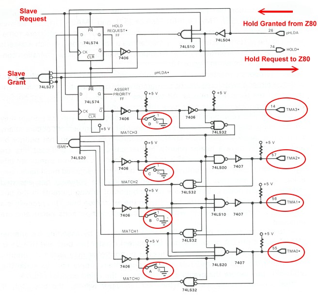
The S100 bus founders came up with a very clever circuit  to implement all this in a few IC chips shown here.
 
  TMA Discussions
  
This circuit would be on each slave S100 board. Each slave board has its priority assigned via 4 dip switches.  Any slave requesting the bus (see below) first posts its "Slave Request". If pHLDA is not asserted (Z80 currently has the bus),   and HOLD* is not already asserted the slave will assert its priority via TMA0-TMA3 and take the bus as describe above (pHLDA/HOLD).  The slave will know it has the bus when Slave Grant goes HIGH. 

On those rare occasions where two (or more) slaves  apply at exactly the same time the TMA0-TMA3 lines become relevant.  Each slave boards dip switch's priority is compared with the TMA0-TMA3 lines.  These are open collector lines.  The highest dip switch combination at that times "wins" and that slave gests to raise its Slave Grant signal and proceed to utilize the bus (after it gets back the usual pHLDA* from the master/Z80).    

One very important point to remember.  A slave in this scheme cannot call another slave -- higher or lower.  Once a slave has the bus the bus belongs to that slave. 

Now there is one other very important process we must consider in this transfer process.  The master/Z80 cannot immediately drop all its address lines , status lines and control lines and expect the slave to glitch free pick them up.  There has to be a very carefully laid out process for the transfer of power.  This is done in an agreed upon very well defined process in the IEEE-696 specs. 

The transfer process is carefully synchronized by the bus clock PHI (pin 24).   This can be (these days) 2-10MHz.   To implement this transfer process two signals are always synthesized on both the master/Z80 and slave boards called XFERI and XFERII to regulate this process.  First it's important to realize that these signals themselves never appear on the S100 bus. In fact on some IEEE-696 boards they really only effectively exist with a GAL (e.g.. the CompuPro 8085/8088 board).   In fact in hardware they can be active high or low. Most boards chose low. Different manufactures called them different names on their circuit schematics. XFERI & XFERII is what the IEEE-696 specs call them. It's what they do that is important.

On the bus master (Z80), on the lowering edge of the next clock cycle after it grants the S100 bus to the requesting slave it lowers XFERI*.  This has the effect of inactivating all the Address line, Status lines and Data Out line buffers on the master/Z80.  This is implemented by lowering the S100 bus ADSB*, SDSB* and DOSB* lines.  At the same time also one clock cycle after receiving control of the bus the relevant slave board lowers its XFERI* line.  This activates only its S100 bus Control lines driver (pSYNC, pSTVAL, pWR* and pDBIN).  At this point BOTH the master and slave are now driving the bus control lines.  Because for a brief moment there may be a driver conflict on some boards (and for all S100Computers boards),  the output from these lines on to the bus goes through a 10 Ohm resistor. 

On the next rising edge of the above clock cycle the bus master activates XFRTII*. This ends up inactivating its control lines buffer via the S100 bus signal CDSB*.  The master is now effectively now not on the S100 bus.  Over on the slave,  the rising edge of the above clock cycle the bus slave activates XFERTII*. This activates the slave Address lines, Status lines and Data Out line buffers and the slave now has complete control of the bus.  Any board in the bus can always tell who is in charge by looking at the TMA0*-TMA3 lines.  For example for our MSDOS Support board we normally don't want that boards ROMs visible on the bus unless there is an 8086-80486 style CPU active.  Its of no use for example to a 68030 using up a RAM address space window.  On that board it can be configured to only activate  the onboard ROMs when TMA0* is low.

S100 Bus Master/Slave Transfers - In Practice.
In actual reality as far as I know the above scheme was never implemented in full by a major S100 bus board manufacture. Even the well known S100 board manufactures like CompuPro and Intersystem's did not implement it on their IEEE-696 CPU boards.  Most CPU boards were in fact bus masters only. If there was a second CPU it was on the same board (e.g. a 8085/8088 Z80/68000 or Z80/80286).

The second problem was the IEEE-696 specs did not really address the clock speed of the two different CPU's.  In most cases the slave CPU is capable at running at a different (higher) speed than the bus master. It is desirable to up the speed of the slave once it has the bus.

Finally while 16 slaves are nice the reality is two or three different slave CPUs is all that is usually needed.  What is actually really needed is the ability of a slave to itself call a lower further slave. A slave of a slave if you like.  This for example could be a slave CPU board that uses a DMA or FDC controller.  The approach S100 bus manufactures used varied but in general were along the following protocol.  This is the approach for all our S100Computers CPU boards use and will be described here:-

The S100 bus can have (in theory) up to 4 slaves. Which slave gets to control the bus is defined simply (and completely) by software in the master/Z80 ROM.   A user defined I/O port is used to activate the process. This can be done in in either of three different ways.

1. Using our V1,V2 or V3 SMB board one just inputs from I/O port EDH. Depending on the boards jumpers one of the TMA0-TMA3 lines is lowered.
2. Using our V2 or V3 SMB  board the software outputs a bit pattern to I/O port EEH. This lowers a specified TMA0*-TMA3* line via software. 
3. On the slave board itself,  either in a GAL or in a CPLD one of the TMA0*-TMA3* lines is lowered again by inputting from a S100 bus I/O port.   

The actual port address above is user defined. The default is EDH and EEH.  However for number #3 it can be a different port number for each slave board. In this way differing TMA0*-TMA3* lines can be pulled down.   The key thing to remember is nothing happens to the slave CPU until the above I/O port process takes place.  For #3 the GAL or CPLD actually raises a slave board local "TMAx" signal which itself is jumpered to one of the TMA0*-TMA3* lines.

Lets follow a typical master/slave transition: 
         For method #1 & #2, the master/Z80 ROM code recognizes the I/O port request.  It lowers one of the  lines.  
         The relevant line TMA0*-TMA3* is jumpered to TMAx on the slave board 

         For method #3, the slave board GAL/CPLD code recognizes the I/O port request.  It raises the TMAx line directly.
         This line is however jumpered to one of the TMA0*-TMA3* lines. 

In all cases two things must happed.  TMAx must be raised and a unique TMA0-TMA3* must be lowered. 

It is the effective of raising the TMAx that initiates the master slave transfer from here on in. From a hardware point of view the master/Z80 does not know/care who is taking over the bus.

On the slave board the raising of TMAx causes a pHOLD* request to be placed on the bus.  After the master/Z80 replies back to the slave with pHLDA,  the bus master/Z80 on the lowering edge of the next clock cycle grants the S100 bus to the requesting slave which lowers its (internal) XFRERI* signal.  This has the effect of inactivating all the Address line, Status lines and Data Out line buffers on the master as we described above.  At the same time also one clock cycle after receiving control of the bus the relevant slave board lowers its XFERI* line.  This activates only its S100 bus Control lines driver (pSYNC, pSTVAL, pWR* and pDBIN) -- again as we described above.

On the next rising edge of the above clock cycle the bus master activates XFRTII*. This ends up inactivating its Control lines buffer via the S100 bus signal .  The master is now effectively now not on the S100 bus.  Over on the slave,  the rising edge of the above clock cycle the bus slave activates its XFERTI*. This activates the slave Address lines, Status lines and Data Out line buffers and the slave now has complete control of the bus.

The slave can remain in charge of the bus indefinitely from here on in.  When finished the whole process is unwound.  The slave releases pHOLD* the XFERII* and XFERI* signals are raised (in the reverse order in which they called on the master and slave boards) and the master picks up exactly where it left off on the next (Z80) opcode. 

On all S100computers.com we have two optional options.  First when the slave XFERII* signal is activated it not only places its pSYNC, pSTVAL, pWR* and pDBIN signals on the bus it also generates and places its own PHI signal on the bus.  Likewise when the XFERII* signal activates the master/Z80 PHI signal is removed from the bus. This allows for a variable bus clock rate.  The later S100 IEEE-696 CPU boards had a jumper to allow this (e.g. the Intersystem's Z80 VII board).

Second some of the S100Computers slave CPU boards could be jumpered to facilitate the above slave of a slave configuration.  This is a fairly complex process and definitely not for everybody.  It can be done in hardware as we did for our 80286 board and at least in theory with our CPLD driven more recent CPU boards.

There are a number of other ways the above handshaking process could be done.  For example you could implement  the XFERI* and XFERII* on the bus master just by sending out the ADSB*, SDSB* DOSB* and CDSB* from the slave board. 

  
S100 BUS 8 & 16 BIT DATA PATHS.
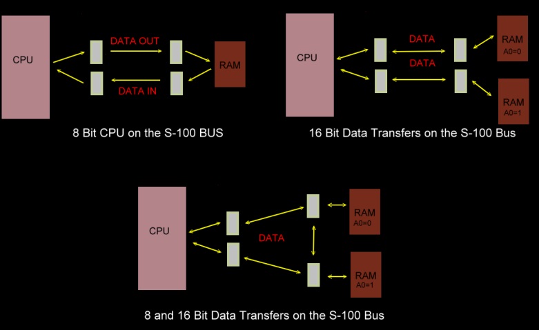
The S-100 bus was designed around the 8080 CPU. This CPU has a bi-directional 8 bit data path, however because Ed Roberts wanted to control it via a series of front panel switches, the CPU data bus was broken out into separate 8 bit Data In and Data Out paths on the S-100 bus.   This worked fine. RAM boards had their RAM chips connected to both data paths and I/O boards were likewise connected.   It was a somewhat inefficient setup but it worked (all for a simpler front panel).   The first diagram below shows the basic layout.
  
  8-16 data Paths
   
When 16 bit CPU's came along things got more complicated.  All 16 bit CPU's have a 16 bit bi-directional data path. They can interface directly to RAM chips that are 16 bits wide or two 8 bit wide RAM chips. In the early 80's the latter type of RAM's were much more common. Two 8 bit wide RAM chips differing only in address line A0 (0 or 1), would be connected to the 16 bit bus.  The S-100 Data In and Data out lines were utilized together as a single bi-directional 16 bit bus and were connected via buffers to the CPUs 16 data line pins.

Now if all you were going to use was such a 16 bit CPU that would be fine. But such a setup would not work with older 8 bit RAM cards or indeed with any I/O cards which also expect a split 8 bit interface.

The solution was simple and elegant and the heart of the IEEE-696 standard. For 16 bit systems the bus behaves as a 16 bit bidirectional bus. For 8 bit systems a bridge buffer on each RAM board transfers the data coming and going to the board over separate 8 bit data lines depending on whether it's address is odd or even. If we have 8 bit data coming to the board on an even address, it travels on the "Data Out" path and goes directly to the A=0 RAM bank.  If instead the 8 bit data is destined for an odd address it arrives as before at the RAM board top buffer but then is dropped down to the lower A0=1 RAM bank  via a bridging buffer.

If the 8 bit CPU wants to read a even address it activates this buffer in the opposite direction so the RAM A=0 bank data is shifted down to the S-100 data in lines. If the 8 bit CPU wishes to read am odd RAM address the A0=1 RAM bank data travels directly to the  CPU on the Data Out bus.

The hardware logic to do this is quite tricky. You need to factor in if we have a CPU read or write, if the data is 8 bits or 16 bits wide and if the destination address is on an even or odd address line.  (Fortunately no common 16 bit CPU transfers 16 bit data on an odd address line).

Back in the mid 80's companies like CompuPro and Macrotech implemented this logic in ROM like chips called
PAL's. While some of our earlier RAM and CPU boards utilized 74LSxxx chips, all our more recent boards utilize GALs of a CPLD.
  

This page was last modified on 05/30/2022