An SPI Master Controller Interface Demo using a Cyclone IV FPGA.
We will now go up a notch in circuit complexity we will add to our S100 bus
FPGA Prototype board. Here we
will construct an FPGA SPI interface and use it to communicate with a simple
chip Digital Potentiometer.
This is a simple IC device which outputs a voltage level (in this
case), from
0-5V, depending on
an 8 bit value of
0
to
FFH sent to it
over a simple 4 wire SPI connection.
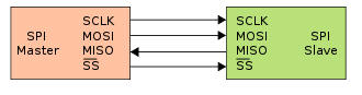
Introduction SPI
The Serial Peripheral Interface (SPI) is a synchronous serial communication
interface used for short distance communication. It is primarily used in
embedded systems. The interface was developed by Motorola in the mid 1980s.
Typical applications include SD cards and LCD displays. SPI devices communicate
in a full duplex mode using a master-slave architecture with a
single master. The master device originates the
frame for both writing
and reading to/from the slave(s). Multiple
slave devices can be supported through selection with individual slave select
(SS) lines. SPI is minimally a four-wire serial bus.
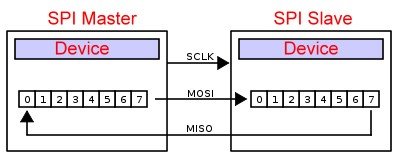
To begin communication, the bus master starts the clock, using a frequency
supported by the slave device. Typically this can be in the 100's of KHz range.
The master then selects the appropriate slave device by lowering that slaves SS
input. If a waiting period is required, such as in for an analog-to-digital
conversion, the master must wait for at least that period of time before issuing
clock cycles. This has to be agreed upon in the programming software.
The master then sends a bits on the
MOSI line and the slave reads them. At the same time
the slave sends bits on the MISO line to the master. This sequence is maintained
even when only one-directional data transfer is intended.
Its important to appreciate two things.
1. The sending and receiving data to/from the slave is completely
linked. There is just one loop like circuit with two shift registers (see
below).
2. The actual data format is completely determined by the
software in the master and slave. The number of bits transmitted can be 8,
16, 32 etc. In theory any number.
Most commonly, the data is in 16 bit packages. The first 8 bits
are used to control the device, the second 8 bits are the actual data.
However its very important to appreciate that the protocol is completely
fluid. You must carefully read the SPI device datasheet to determine the exact
nature of the interface and what each bit in a CMD code does. Worse, the master must also configure the clock polarity and phase with
respect to the data. Motorola SPI specification names these two options as CPOL and CPHA
respectively, and most vendors have adopted that convention. Getting into the
weeds:-
CPOL=0 is a clock which idles at 0, and each cycle consists of a pulse of 1.
CPOL=1 is a clock which idles at 1, and each cycle consists of a pulse of 0.
CPHA=0, the slave captures the data on the leading edge of the clock cycle.
CPHA=1, the slave captures the data
on the trailing edge of the clock cycle.
When the transmission is complete,
the master stops toggling the clock signal, and typically deselects the slave.
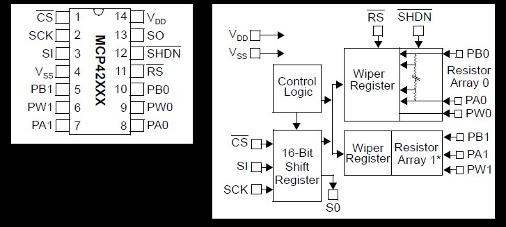
On the slave side of things we will use a very simple SPI device, a
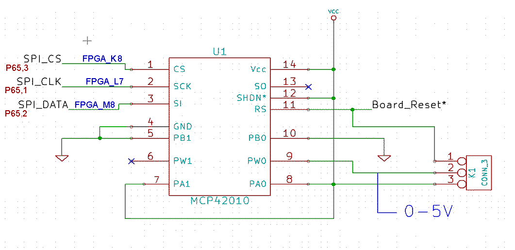
Microchip MCP42010 Digital Potentiometer.
We will use the PDIP Dual version:-
In the FPGA code below, depending on the 8 bit value fed (via the
SPI connection) to pin 3, a voltage value ranging from 0 to about 5V will appear
on pin 9 (and 6). While not needed in this case, it is interesting to
note that the basic clock signal is a high frequency, running in this case at 400 KHz.
The FPGA SPI Code.
There are numerous examples of building a FPGA SPI interface on the web.
As a beginner, frankly I found a number of them overly complex and/or confusing.
Fortunately I discovered a simple and well explained example by Scott Larson
here. In that example the SPI FPA code is in VHDL. Fortunately
the code was designed using Quartus II. So in line with all our previous
examples we simply take VHDL code and convert it to a block diagram (a
.bdf file).
To recap, we do this by loading up the VHDL text file (spi_3_wire_master.vhd)
and from the file menu drop down to Create/Update, Create a symbol file. The new
symbol file module will then be in the Project dropdown menu.
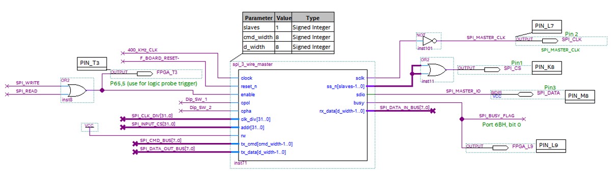
Here is the core
of the spi_3_wire_master
bdf module:-
There are a number of simple inputs to the module:-
This is a nice very adaptable SPI module. Overkill for our demo here. Most of
the signals are fairly obvious. clk_div is an input
that can be up to 32 bits wide to be used as the clock input divider.
Here (and often) we simply deliver the final clock signal directly so (clk_div
= 0). In our case
400KHz is generated in out PLL frequency generator. See the top of the .bdf
file entry. Likewise the number of slave devices is a 32 bit input.
We will use just 1 slave device. We will use an 8 bit input for SPI
control commands (tx_cmd), and also an 8 bit input for data (tx_data). In
this simple example we will not actually be using data returned from the SPI
slave.
It important to appreciate that the way this module works is that the cmd and data
inputs (8 bits each) much first be latched and stable as inputs to the module.
The actual SPI transmission then takes place when
enable is pulsed low. However
its essential this pulse only occurs on the rising edge of the clk input.
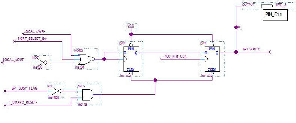
In order to insure this, we need the following logic:-
The S100 port write signal (pWR*)
is narrow and unsynchronized with the 400KHz clock signal. We must latch
it and pass it on to the SPI module as
enable on the next
rising edge of the 400KHz clock signal. While not used here, one would do the
same for SPI data reads.
We will use four S100 bus ports to interface and
control the SPI interface. We will use a 74139 library module to brake up the
address lines
A0 and
A1 into 3 port
selects.
68H, 69H, 6AH.
In our .bdf file we will use port 68H
to provide a latched S100 bus output to the SPI tx_cmd
input. We will use port 69H
to provide a latched S100 bus output to the SPI
tx_data input. We will then use
port 6AH to pulse the enable signal.
This will initiate the actual data transmission to the SPI slave. The SPI
module and slave device will actually require time to transmit the data. During
this time the
pi_3_wire_master busy
line will go high. This line can be read as bit 0 from input port
69H. In our example below we will not
require this since we are manually/slowly sending data to the SPI slave. However
the signal is used to reset the above SPI_WRITE FFs.
Set SW1 OPEN (cpol
HIGH)
Set SW2 CLOSED (cpha LOW)
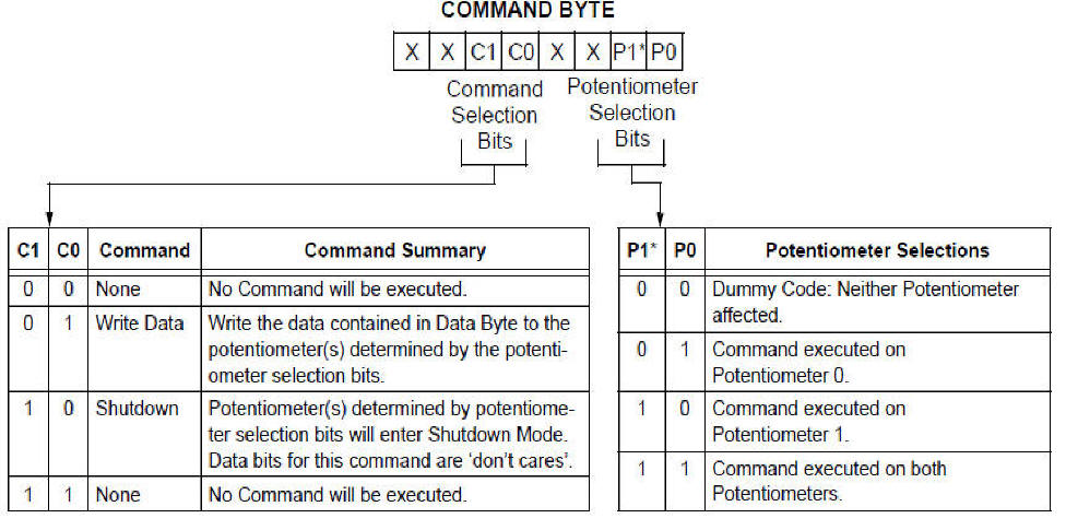
When the Microchip MCP42010 Digital Potentiometer powers up the
potentiometer will be in its mid position and we will see a voltage of
~2.5V on its pin 9. We can drop this
voltage to 1.25V by the following three Z80
monitor port output commands:-
QO68,DF
QO69,40
QO6A,00
You need to study the MCP42010 data sheet to see that
BD selects both potentiometers with a data
write.
If instead we sent
QO69,FF
the voltage would be ~5V.
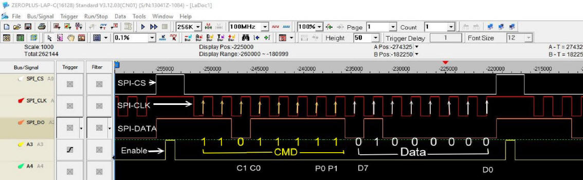
Let us take a logic probe and analyze the actual signals. Here is an
example triggered on Enable going high.
The cmd data is sent first. 8 bits, bit 7 to bit 0. Each SPI bit is
clocked in upon the rising edge of the SPI clock.
The 8 data bits are
sent. In this case
40H. Here is a
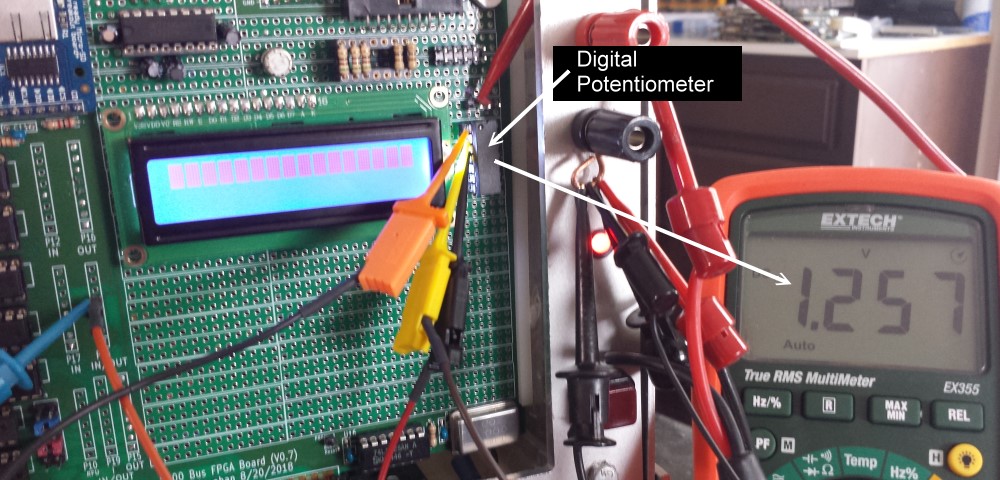
picture of the actual board setup.
Here the simple board schematic
Again this is a very simple example of using our Cyclone IV to interface an SPI
device.
Please study the files below to understand completely what is going on.
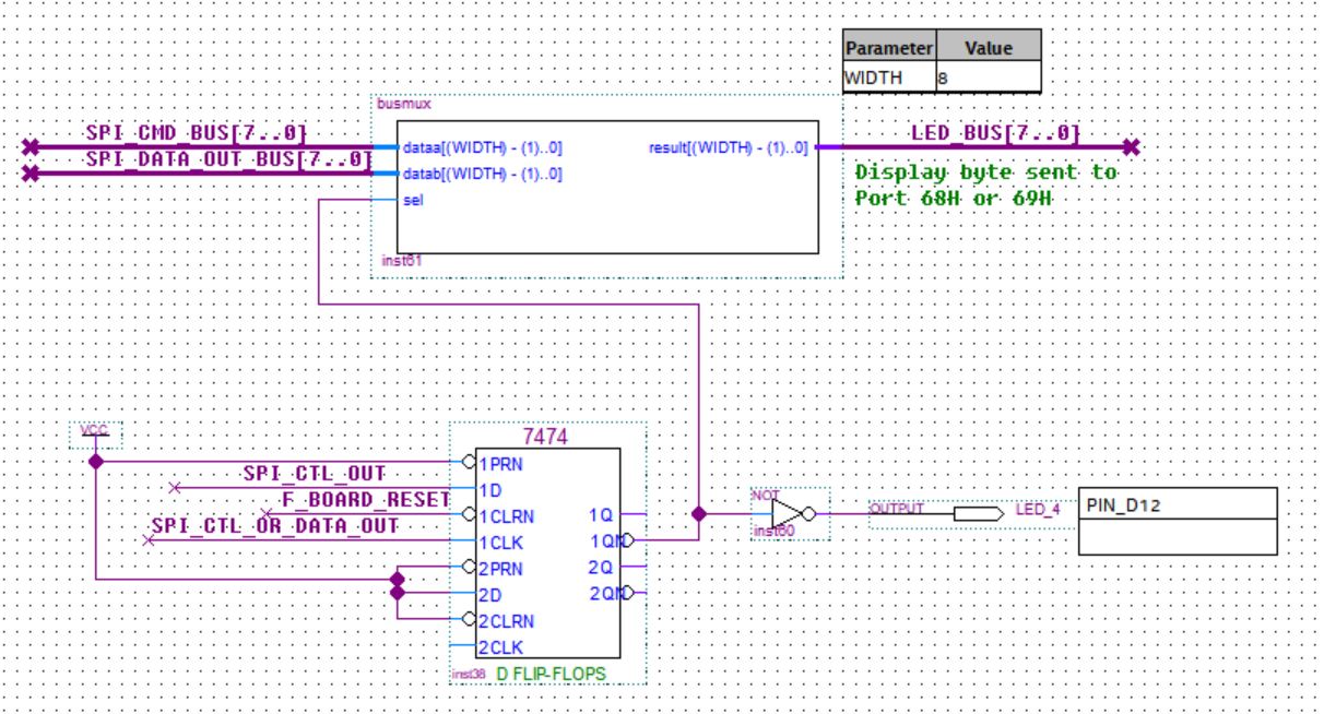
One nice extra addition is to have the boards eight LED's display latch the
data bytes sent to the tx_cmd
or tx_data ports.
Since the are two possible output ports we need to display the last byte sent.
We do this using a 2:1 MUX as shown here.
Bugs
Keep in mind that the Board_Reset FPGA input pin is the S100 bus
Slave
Clear not the system wide
Reset line.
MCP42010.pdf
(V1.0 11/25/2018)
SPI_Master.ZIP
(V1.0 11//25/2018)
SPI_3_wire-master.vhd
(V1.0 11/19/2018)
This page was last modified on
12/26/2018