An SPI Master Controller Interface Demo using a Cyclone IV FPGA.
Here we
will inprove on our earlier FPGA SPI interface and use it to communicate with a variable
number of of data bits. This can be 8, 16, 24, 32, 40 or 48 bits. Long SPI
continuous data streams are for example requires to interface SD Cards. These require 6 byte commands.
Unlike the I2C interface the SPI
clock cannot be stretched. You must have all the data bytes setup before you
start.
If you have not done so already, please read the introduction to the
SPI interface before going further.
To recap, to begin communication, the bus master starts the clock, using a frequency
supported by the slave device. Typically this can be in the 100's of KHz range.
The master then selects the appropriate slave device by lowering that slaves SS
input. If a waiting period is required, such as in for an analog-to-digital
conversion, the master must wait for at least that period of time before issuing
clock cycles. This has to be agreed upon in the programming software.
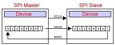
The master then sends a bits on the
MOSI line and the slave reads them. At the same time
the slave sends bits on the MISO line to the master. This sequence is maintained
even when only one-directional data transfer is intended.
Its important to appreciate two things.
1. The sending and receiving data to/from the slave is completely
linked. There is just one loop like circuit with two shift registers (see
below).
2. The actual data format is completely determined by the
software in the master and slave. The number of bits transmitted can be 8,
16, 32, 48 etc. In theory any number.
While the most common format is data is 16 bit packages, however, there are many devices
that require many more clock pulses.
I took our original FPGA 16 bit interface and modified it such that a user
defined variable number of bytes can be processed. This required a
modification of Scott Larson's code described
here. I separated the actual bidirectional SPI data line into a
separate MOSI and MISO line. I added a new 3 bit input that controls the
number of bytes processed. Here is the core FPGA circuit.
You will note that now the module data input is a single 48 bit wide data bus.
Gone are the separate two 8 bit "CMD"
and "Data" bus
input lines. Likewise the data received can be up to 48 bits wide.
The actual data with is controlled by a 3 bit input
BYTE_COUNT.
Outputting to port
6EH the following
gives:
QO6E,01
1 byte of SPI data
QO6E,02
2 bytes of SPI data
QO6E,03
3 bytes of SPI data
QO6E,04
4 bytes of SPI data
QO6E,05
5 bytes of SPI data
Outputting any other value (including 0) always outputs 6 bytes of SPI data.
There is also an option to address two Slave devices. If bit 7 of port 6EH is 0
then Slave0 is addressed. If it is high, Slave1 is addressed.
The actual data bytes are sent via ports
68H, 69H, 6AH, 6BH, 6CH & 6DH
for the data and 6EH
and 6FH
for the controls.
The first byte being 68H the first byte to appear on the SPI line, all the way
up to, if required 6D the last byte (bits 41-48).
So to use our earlier Microchip MCP42010 Digital Potentiometer
we would send out the following Z80
monitor port output commands:-
QO68,DF 8
bit CMD byte to MCP42010
QO69,40
8 bit DATA byte to MCP42010
QO6E,02
Tell interface we need to send a 16
bit SPI signal (on the default, slave0 device).
QO6F,00
Actually send/write the data to the
MCP42010
The actual logic probe signals should be exactly as we saw
previously.
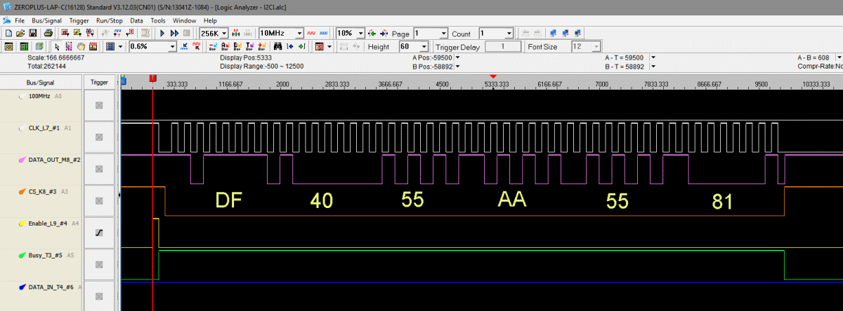
Here is an example of an SPI output of 48 bits (6 bytes) of
DF,40,55,AA,55,81.
To obtain this signal from your Z80 Master monitor type:
QO68,DF
QO69,40
QO6A,55
QO6B,AA
QO6C,55
QO6D,81
QO6E,00
<-- Send 6
Bytes. To Slave0
QO6F,00
<-- Activate the write process
Please see
here for more information on interfacing an SPI interface with an FPGA
Bugs
Keep in mind that the Board_Reset FPGA input pin is the S100 bus
Slave
Clear not the system wide
Reset line.
MCP42010.pdf
(V1.0 11/25/2018)
SPI_Master.ZIP
SPI_3_wire-master.vhd
This page was last modified on
08/01/2019


