| Jumper |
Function |
| JP5 |
Normally closed. Generate the S100 bus MWRT signal on this board when it is active. |
| JP1 | Normally closed. Generate the S100 bus 2MHz Clock signal on this board when it is active. |
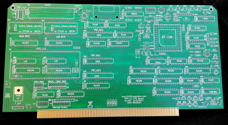
| P13,P14 |
These jumpers define the Baud rate, parity and stop bits for the
UART. See above for a picture |
| P11 |
Jumpers to accommodate RAM or ROM chips. For RAM J11 1-2. For
EEPROM's leave open. |
| JP4,JP5, JP6,JP7 | Normally all open unless the board is a bus master. |
| JP13,JP15 |
Normally closed to utilize the S100 bus
Phantom Line. Normally no need for JP15 |
| K2 & K3 |
RAM/ROM OE* & WR* signals. For RAM jumper both 2-3. For EEPROM
jumper both 1-2. |
| K1 |
Normally 1-2 |
| K9 |
Normally allow S100 bus
wait states with 1-2, During build use 2-3. |
| K7 |
UART Select,
Set 1-2 for core circuit testing. Normally 2-3 |
| K5 |
For slave mode 1-2 |
| JP9 |
Jumper after the CPLD is programmed |
| K6,JP12 |
Set 1-2 and jumper JP12 |
| P8 |
Set 1-2 and jumper JP13 |
| P9 or P17 | CPLD JTAG programming socket.
For Rockfield Research 1508 programmer use P5. Pin 1 is bottom left. |
| P22 |
Spare input CPLD pin |
| K3 & K4 |
XFERI & XFERII,
In slave mode, 2-3 |
| P10 |
S100 Bus TMA line to activate board. Normally 1-2 (or 3-4)
closed. |
| JP19,JP20,JP18,JP20 |
Jumpers to patch connections to extra S100 bus lines. Normally
all unconnected |
| P22 |
Inputs from S100 bus Interrupt vectors. Normally all open. |
| K10 |
This can be a mini-switch or jumper to determine where the
PDP_MON monitor data I/O is sent |
| P2 |
This a serial port connector for the UART with a pinout like our
Serial board. If the DB9 socket is used it must be jumpered as
described above. |
| JP8, JP11, JP10 |
Normally all open. Used only for a bus master |