S100 Computers

HomeS-100 Boards HistoryNew BoardsSoftwareBoards For Sale
ForumOther Web SitesNewsIndex  
  
An S-100 80286 CPU Board.
  
 
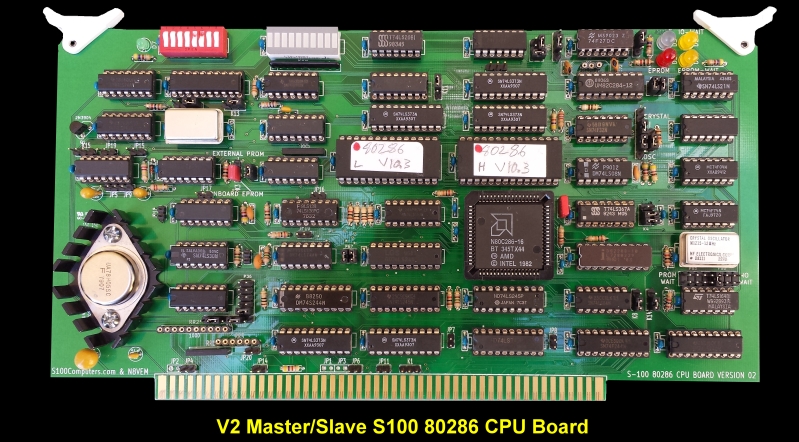
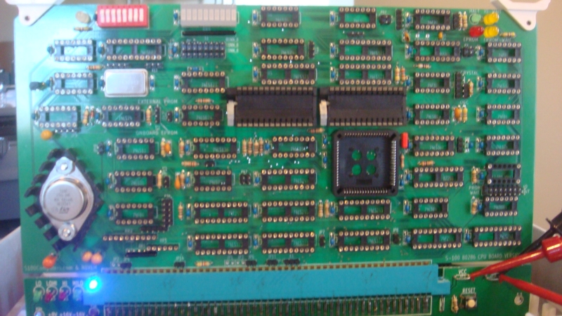
  Picture Of 80286 V2 Board


INTRODUCTION
A number of the later S-100 board manufactures had their own 80286 CPU card.  These boards moved the S-100 bus capabilities into the 16 bit world and past the 1MB memory addressing capability of the 8086. Software was usually either CPM86 or a variation of MS-DOS.  This was at the time the IBM-PC and PC clones began to dominate the area and so IBM-PC compatibility became the rage. Few succeeded in true software/hardware compatibility. Only the CompuPro and perhaps Macrotech based board systems came close to achieving this goal.  One of my goals will be to do this.

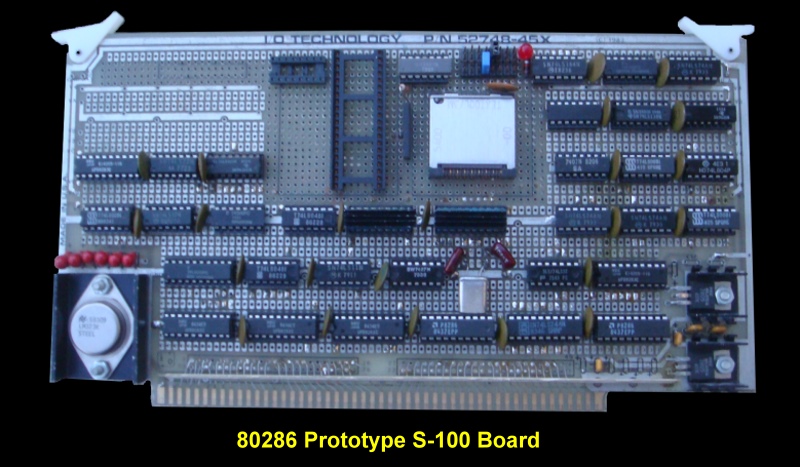
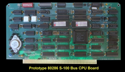
I built a very early S-100 80286 prototype board back in the early 80's.  Here is a picture of that board:-
  
Early 80286 Prototype Board


The board (still) works well up to about 5Mhz in my system.  It runs fairly hot however with these old chips -- thus the heat sinks attached to 82284 and 82288 chips!  Because of space limitations there was no on board monitor EPROM. Instead the board booted directly from RAM/ROM on the S-100 bus at FFFFF0H.  BTW, this is where our Z80 CPU board with its ability to address 1MB of RAM came in real handy. Because one can easily deposit 80286 code at that area in RAM for board testing etc. 

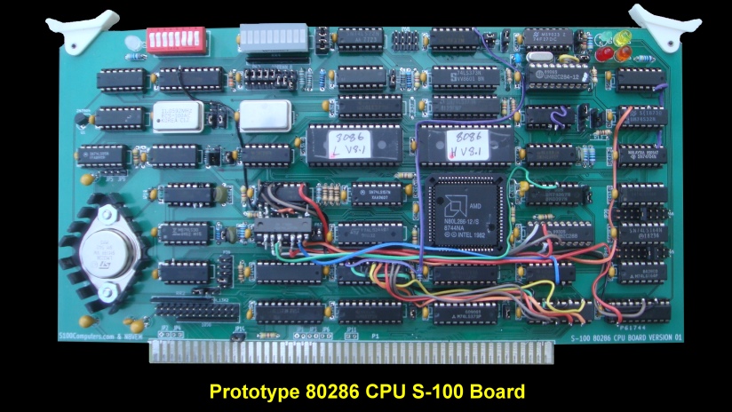
However I felt any new S-100 80286 board should be capable of running at a higher speed, something in the range of 8-12MHz using the later 80286-12 chips.  Consequently I modified the above board fairly extensively.   I decided to place an onboard pair of EPROMS on the board.  Using the schematic shown here, I drew up the following early prototype. Here is a picture of that board:-

V1 80286 Prototype Boadr

The board need some major modifications, thus the wire patches. These of course will be removed in the next version of this board.  There are more support chips on this board because we are now including the two EEPROMS. As we shall see below these two chips require their own address and data buffers (5 chips).  The basic circuit for this board is based on our now tried and true 8086 CPU S-100 board. The two boards have about 90% of the key circuits in common.

The Circuit
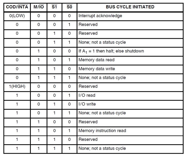
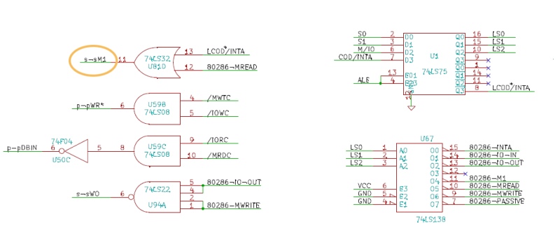
Let us look at the boards basic circuit components one at a time.  It is important to do this because we will need a reliable 80286 board to move up to a 80386 or higher board later.   At first glance the 80286 interface (the 80286, 82284 & 80288 chip set) seems similar to the 8086 corresponding chip set (the 8086, 8284 & 8288).   However there are some subtle but important differences. The major one being the 80286 status signals (S0, S1, M/IO* and COD/INTA*) now replace S0, S1 & S3 for the 8086 in its MAX mode.  Not only that, because the 80286 puts out "Reserved" status signal combinations, one has to latch the above signals with ALE to generate the corresponding valid S-100 status signals.  Here is a table of the 80286 status signals:-
  
 Status Signals Table
   
You will note that with the exception of the "Memory Instruction Read", (M1) we need only decode S0,S1 and M/IO* to generate unique S-100 status signals. The S-100 sM1 signal (pin#44) is really not much used in S-100 systems but we will synthesize it anyway with the following circuit:-
 
 SM1 Status Signal
 
  
The other status signals can be generated with a 74LS138 as shown above.  Note how we use the 74LS75 (U1) to latch the status signals that are then decoded by U67.
  
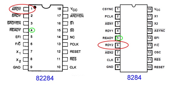
The other way the 80286 differs from the 8086 is in how it looks upon the "Ready line".  The ready signal going to the 80286 (pin #63) adds wait states to the CPU if it is high at a certain point in its bus cycle.  The 8086 in contrast, has it such that if its ready pin (pin #22) low it will add wait states.  On top of that the 80284 clock controller has a different pinout and in fact two different types of ready inputs. The so called "Asynchronous Ready input"  (ARDY*) and a "Synchronous ready" input (SRDY*).  If the latter can be clocked/synchronized with the CPU clock, you can gain a little more time in advance letting the CPU know a wait state will be required. I did not use this function on this first prototype board but will on the next.  Here is a diagram of the two clock generator chips.
     
 Clock Chips
  
 
The Master/Slave Transfer Logic
This board upon power on or reset will normally exist on the S-100 bus as a slave CPU board. That is it will be inactive while the Master CPU (usually a Z80) board is active. (It can be configured as a Master itself, but lets pass on this for now).   Please look at this diagram:-
 
 Handshake Signals

  
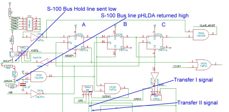
In this configuration the Intel 82284 Clock Controller holds the 8086 in a permanent reset state (its pin 11 is low).  The S-100 bus allows for up to 16 slaves (CPU/DMA) boards. They are selected by the four S-100 lines TMA0-3 (pins 55-57 & 14).  I will use the TMS0 line here.  To activate the board we lower TMA0 (typically by outputting a bit from a port elsewhere on the bus, e.g. the SMB, but this could even be a bounce less switch).  This lowered signal is passed along step by step the three 74LS74 flip flops A,B & C. A and C are clocked by the S-100 bus master clock Phi.  The output from flip flop A is sent back to the bus as a low on the S-100 line HOLD* (pin 74). This tells the Z80 another board wants the bus. When it is ready it raises the S-100 hold line pHLDA which clocks the flip flop B. This is then clocked (by Phi) through flip flop C and eventually raises the Res* pin 11 on the 8284. This releases the 80286 from its reset state. The output of flip flop B also puts out the important signal XFERII which amongst other things allows the "new" Phi clock signal for the 80286 to appear on the bus.  Meanwhile at this time all the Z80 status, data, address and control lines are tri-stated.  It's as if the Z80 no longer exists on the bus.

Now it should be pointed out that the original IEEE-696 specs allow for only 1 master clock on the bus. In real world practical systems this usually meant the Z80 clock.  It was not long however until almost every S-100 board manufacture  adapted a modification (like that above) that allowed the slave CPU to supply its own (faster) clock.  This is what I will use in all our Slave S-100 boards.  It is important also to remember that this board cannot itself transfer control to another slave board (for example a DMA controller) the board/software must refer back to the true S-100 bus master.  This is how the IEEE-696 protocol was setup.
 
The actual frequency used by the 80286 is high, at least by the old S-100 bus standards, (typically 10-12MHz). This requires a good motherboard/bus structure preferably with some type of line termination.   However before you get too excited about these high clock frequencies remember the first thing the 80286 does internally is divide the incoming clock by two for its actual operation.  So a 12 MHz 80286 is operating like a 6Mhz 8086.  Of course the 80286 requires less clock cycles for most instructions.

BTW, unlike our earlier 8088 and 8086 CPU boards which have the same above handshake/bus switching circuitry, this board has extra circuitry that may be of interest to the more sophisticated users....

Let me explain, in the IEEE-696 specs., there can be only one master that transfers control to slave bus devices (such as the above 80286 in our case).  Now it turns out that the 80286 itself has the ability to activate its own DMA device with its own HOLD and HLDA pins. The IEEE-696 standard has no protocol to handle this.  I have added circuitry to accommodate this HOLD within HOLD on the bus by using two of the IEEE-696 non-defined lines (NDEF3 & NDEF1).  At some stage I may utilize a powerful DMA controller board to accommodate this capability.  The circuit is centered around U97, U98, U79D and U63B in the schematic below.

Most users can completely ignore this section.


Status and Control Lines
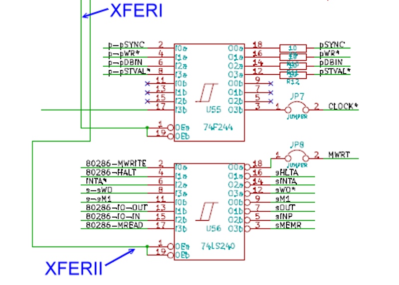
It is absolutely critical that the above transition takes place in an orderly fashion where at no time are any of the S-100 bus lines left floating -- no matter how short the time.  This is accomplished in a two step process called XFERI and XFERII.  In XFERI the Z80 bus status, data and address lines are switched over to the 80286 but the Z80 still retains control of the critical control lines pSYNC, pWR*, pDBIN and pSTVAL*.   In this way even though all the other S-100 lines are getting switched over nothing will happen to any of the S-100 boards (if they are IEEE-696 compatible).   No memory will be written to with garbage, no ports accessed etc.  When that transfer is complete, only then, does the second XFERII process take place.  For a very brief period of time the Z80 and 80286 will BOTH be controlling the pSYNC, pWR*, pDBIN and pSTVAL* lines.  (That is why on well designed boards they have 10 Ohms resistors -- to protect the bus drivers).   Once the Z80 signs off (one Phi clock cycle later), the 80286 has complete control of the S-100 bus.
        
 Control Signal Circuit
    

This whole process seems complicate at first and to some extent is,  but a lot of thought, care and attention was put into it by the original IEEE-696 committee to allow for an extremely reliable system.

If you don't quite understand the above, don't worry just look upon the circuits as a "black box" for Master/Slave switching. 


Data and Address  Lines
The 80286 does not multiplex its 24 address lines and 16 data lines like the 8086. While I do not see a reason why in a simple one CPU system, they are normally latched into 74LS373's (in our case U73, U74 & U75) with the ALE (Address Latch Enable) from pin 5 of the Bus Controller (the 82288). 

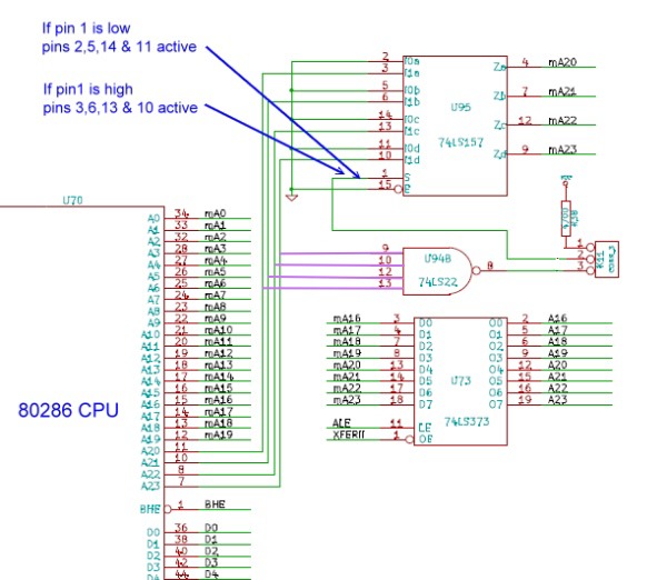
Remember, the 80286 always starts at 0FFFFF0H upon reset. This is at the very top of the S-100 buses memory 16 MB address space. In contrast, the 8086 starts at 0FFFF0H (at the top of the 1 MB address space).  It's usually convenient to write one BIOS/Monitor for both CPU's.  We play a trick on the 80286 in that whenever its top 4 address lines are all high (only at the top 64K of the 16 MB address space), these 4 address lines in hardware show up as all low on the S-100 bus. Thereby an 8086 BIOS/monitor ROM can be utilized.   A two line to one line converter (U95, a 74LS157) is used to accomplish this in the following circuit:-
  
  High Address Lines
  
Jumpering K11 1-2 will of course bypass this option.

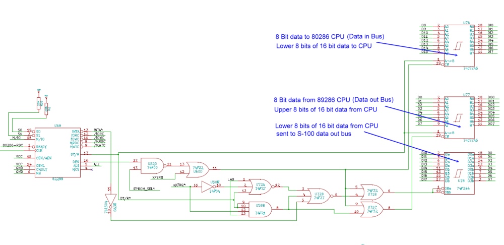
The 16 data lines are of course more complex. Not only must they be bi-directional, but they must splice into the S-100 bus to handle 8 or 16 bit data transfers.  The special IEEE-696 spec. sXTRQ* of the S-100 bus must be utilized to let other boards on the bus know what to expect.   I have discussed at length elsewhere on this site this process. See here.  Fortunately the 80286 has a special pin BHE (Bus High Enable) which greatly simplifies this process. Pin 19 of U84 delivers sXTRQ*  to the S-100 bus.   The somewhat complex circuitry here accomplishes this.
 
 8-16 Bit Data
  

All this would be fairly straightforward if it was not for the fact that the 8086 will input and output either 8 or 16 bits of data. 

The 74LS244, U78, takes care of the transferring both memory and port ODD/upper address IN  8 bit data to the lower byte data bits of the 80286 where it expects to find them.  The circuitry took quite some time to figure out, and for some people it may be best looked upon as a "black box".  It has proven itself to be very reliable in our 8086 board.


The Onboard EEPROM  
As I said above, my original prototype board did not have an onboard ROM.  Instead after a reset it looked at the S-100 bus RAM at FFFF0H.  There are some advantages to this. With a Z80 system that can examine and modify RAM at this location (see here) you can quickly test a board. This will be described below in detail.  However there are advantages to having a powerful on-board EPROM monitor on the board -- particularly if it is to be a bus master and the only CPU in a system.

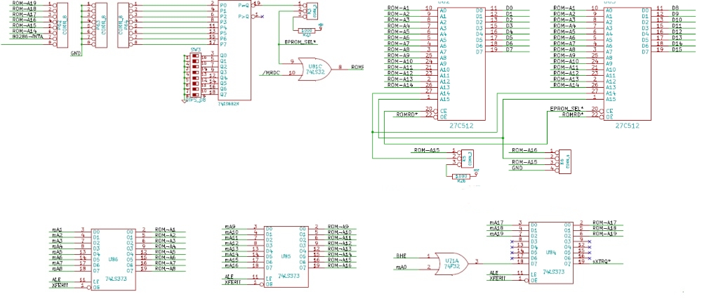
Unfortunately adding an EPROM takes more space than you might expect.  In order to simplify the hardware, first we use two EEPROMS, a high and low byte.  This avoids the need for a BHE pin function since the 80286 will never be a write to this memory location,  (the CPU itself takes care of the data lines for High/Low input data).  Furthermore whenever the 80286 is addressing the onboard EEPROM it must inactivate completely the drivers to the actual S-100 bus.   The EPROM_SEL* signal generated as shown in this schematic does this using pin 13 of U52D, (see above schematic).
  
 EPROM Circuit
   
      
Note how the outputs from the data pins of the two EEPROMS directly drive the data pins of the 80286 once ROMRD* is low.  Note also how EPROM_SEL* inactivates the S-100 drivers in the above previous schematic.  With SW3 the EEPROM can be configured to start at different locations.  However the 80286 starts from a reset at FFFFF0H. So normally we would place the ROMS at say FF8000H. Remember as I outlined above,  one unusual aspect of the 80286 (and higher) CPUs is that after reset while the CS register is set for 0000H the actual address pins point to FFFFF0. Only when we do our first long jump does the CS register match up with the address pins. This allows the 80286 upon a reset to act the same as an 8086. Starting from a software reset location of 0FFFF0H.  So if you are writing 80286 monitor code you can use your old 8086 code unless you do a far jump.  

While on the subject of PROMS/EEPROMS, a number of UV-EPROMs or EE-PROMs are possible using jumpers K5 and K6, I like to use 28C256 EE-PROMS. They are cheap these days and have 150 ns access times.  These are 32K X 8 PROMS.  Generally you don't need all that capacity (remember the PROMS are in pairs),  For my 8086 Monitor I use only the top half of each 28C256 EE-PROM.  So for example when burning (separately) the high and low bytes with the Wellon VP-280 Prom burner, the code would reside at 4000H-7FFFH within each prom.  On our board switch SW3 is configured so the PROM pair appear at 0F8000H - 0FFFFFH.  This is further detailed at the start of the 8086 Monitor listing, see here.


This board in my hands will work (at 12MHz - see below) with any of the S100Computers boards made over the years. It also works with a number of IEEE-696 Memory boards such as the CompuPro 128K static RAM-21 board, the 256K static RAM boards from BG Computers or Fulcrum and the Electrologics 1MB Memory Disk.  I have not tested it with any Dynamic RAM boards. If these boards have their own onboard refresh controller I suspect they would be fine -- at least up to 6MHz.   If however they rely on the Z80 refresh signal (non-IEEE 696 boards), they defiantly will not work.

For this board to run at 12MHz it has to be jumpered for (at least) three wait states for I/O in order to utilize I/O ports on other S-100 boards, (Note no wait states were required in the final production board, see below). Also for reliability a number of the 74LSxx chips need to be changed to the faster 74Fxx types.  These are indicated in the schematic. The Achilles heel of the board is for fast 8 bit reads of memory from odd address lines. The S-100 bus brings this 8 bits of data in to the board on the upper 8 bit (S-100) data lines.  They must be shifted down to the lower 8 bit data bus via U78 and then passed through U75.  This unfortunate "in, across, and then in"  process has a slight timing overhead, so it is important that the logic involved is fast. Thus the use of 74Fxx chips in these areas (U52, U60, U72, U58, U71, U78) on the board.

Realizing that people may wish to use this board with old S-100 boards that have slow I/O access times (old IMASI/Altair 2MHz systems) I added the following circuit that allows up to 4 wait states to be inserted during any S-100 bus Port I/O.  Note these board must have and recognize the S-100 sXTRQ*/SIXTN* signals.  Non-IEEE-696 boards (8 bit only) will not work.
  
 Wait State Circuit
 
     
The IOWAIT and EPROMWAIT lines feed into the RDY line of the 82284 clock generator.  For the 82284  there are two possible ways the ready line can be triggered.  The READY* line (pin 4) acts like the RDY1 or RDY2 lines of the 8284 that is used with the 8086.   It recognizes an asynchronous ready signal. That is the signal can strike at any time within the 80286 clock cycles and be recognized.   There is a second ready signal the 82284 can recognize called the "Synchronous Ready" (SRDY), which must be synchronized with the CPU clock signal that can also be used.  It has the advantage that it can be delayed a little bit more by the bus hardware and still catch the 80286 CPU in time.   The 82284 pins 1 & 2 activate either or both signals.  There are jumpers (P2), on our V2 board to utilize either signal. However I found that at least in my system the Asynchronous Ready signal is fine.


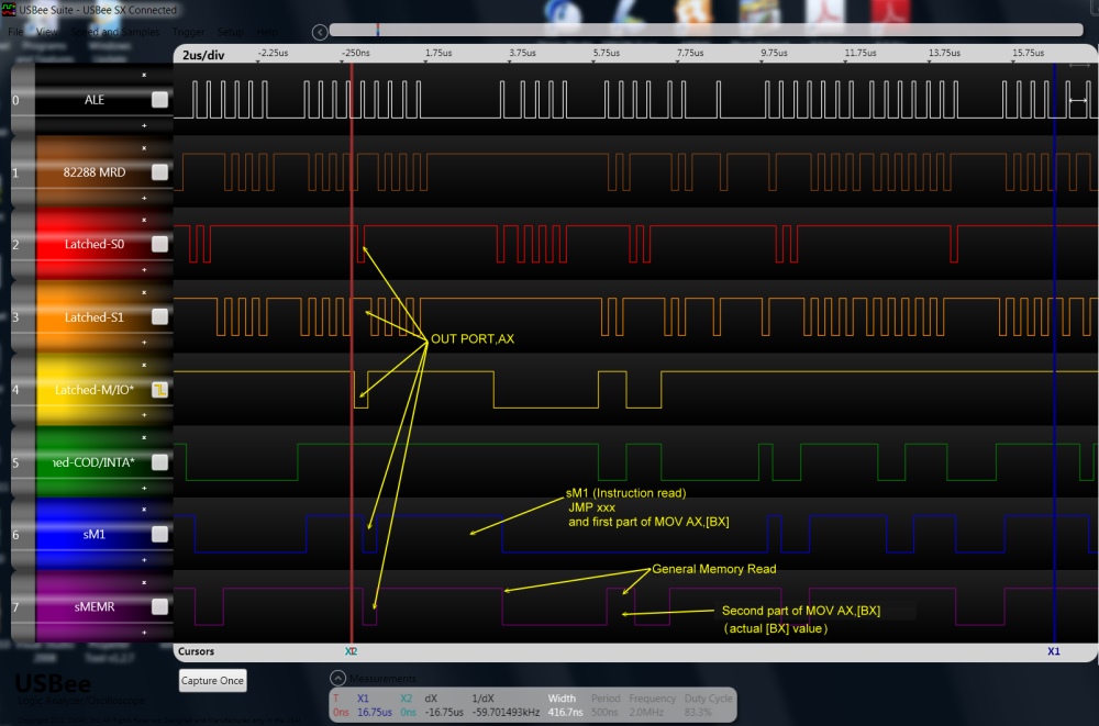
Here are some logic signals on from the board:-

 sM1 & sMREAD Signals

The above picture is for the probe synced on the OUT signal of the code:-

XXX:   MOV    AX,[BX]
          OUT    01H,AX
          JMP     XXX


The first line requires two types of memory reads. The code read (sM1) followed by the actual memory data read in this case. Consequently we have the two sMEMR signals and one sM1 signal.  Note how the status signals line up for the OUT instruction and at this time sM1 and sMEMR are low.

The next example we exercise the following code:-
 
             MOV   AL,33H
XLOOP:  OUT    01H,AL                   ;"3'' to CRT continuously
              JMP    XLOOP

 
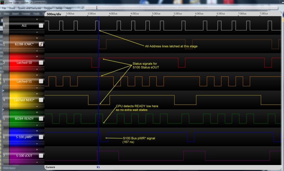
 sOUT Signals
    
Here we continuously output to an I/O port. The CPU status signals S0, S1, and M/IO* generate correctly the S-100 bus sOUT status signal.  This is with no wait state jumpers on P66.  The width of the pWR* signal is 167 ns.  Here is a picture if we add one wait state (Jumper P66 1-2)
   
 sOUT 1W

BTW, don't worry about the irregular top clock pulses. The reason they vary a little is because the data access rate of the PC based logic analyzer cannot keep up fast enough.

Note unlike the 8086 and 8088 CPU boards, because the incoming clock to the CPU is 2X the internal working frequency of the chip, the wait state jumpers signals coming from U87 (74LS164) are different. Except for the first jumper they are in pairs.

The data analyzer gave the WR* pulse width at 12MHz with 0-4 wait states as:-

0 wait states (no jumper) = 167 ns,  1 wait states (P66 1-2) = 333 ns,   2 waits states (P66 3-4) = 500 ns
3 wait states (P66 7-8) = 666 ns,  4 wait states (P66 = 11-12) = 833 ns


as measured for example for the sOUT signal (U56 pin 3).  With this board you can go up to 4 wait states.

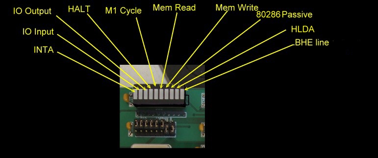
The board can be "single stepped" on the S-100 bus using for example our SMB board.  It is important to remember however that the 80286 has an internal 8 byte "look ahead" queue, so the status signals on the bus actually are slightly ahead of what the 80286 internally is doing. Normally this is not seen -- unless the queue is jumped by an opcode like JMP.  The 10 panel LED Bar at the top of the board indicate the current 80286 cycle.  Here is the breakdown:-
   
LED Bar Signals
  
Also remember if you single step the monitor using the onboard EEPROMS the data bus will NOT show the correct data the 80286 CPU is receiving (this is because the S-100 bus data lines are being bypassed on the board, you are in fact looking at RAM at that location in the S-100 bus!.   The address lines will of course be correct.  As will the data lines if you use an external S-100 bus EEPROM board.

If you put the following code in RAM (or ROM) at FFFF0H:-

B0, 33, E6, 01, EB, FA

and jump to it (reset point for 80286), The 80286 will continuously out the ASCII latter '3" on the console port 1. If you have the S100 Computers SMB and single step the 80286 you will see the appropriate LED's come on as indicated above.

The board has a special LED (labeled D3) that is useful as we shall see below in building the board. If you fill a ROM with 80286 "HALT" instructions (F4H). It should light up if the 80286 reads RAM/ROM correctly. This test is independent of any even/odd 8 or 16 bit logic on the board.    Because of slight differences in the way the 80286 presents its status lines, unlike the 8086 and 8088 boards, the LED "HALT" bar will not remain on. Use LED D3 instead.

The board will work with older 80286's (and 82284's & 82288's) at 6MHz.  To reach greater than 10MHz you need the equivalent chips. However these Intel chips do run hot. It does not seem to bother them, but I always like to run cool boards in my system. Consequently I normally use the CMOS equivalent chips. I use the AMD chip. This is a completely hardware equivalent CMOS chip to the Intel 80286 and is in fact rated for up to 12MHz!.  A good source of these chips is Unicorn Electronics

A second prototype board was done to "fine tune" some of the issue with the first board.  In particular the addressing of RAM above 1MB was not correct. Here is a picture of that board:-
 
 V2 Prototype 80286 

The half size oscillators do save space but I later found they are hard to find and do not exist is a wide range of frequencies. I decided to go back to the full size oscillators.  
 
The Final Production Board.
Based on the above prototype board lessons, a "production board" was fabricated.
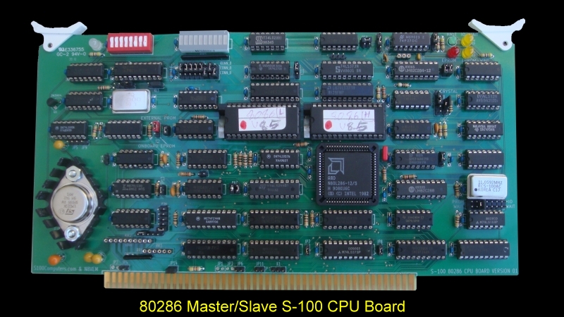
Here is a picture of the final production board:-

 Final 80286 CPU Board 

Step By Step Building The 80286 CPU Board.

Since for many this board may be more complex than what they are used to, I will go into some detail as to how to get it up and running.

The first step is to examine the bare board carefully for scratches or damaged traces, use a magnifying glass if need be. The quality of the boards we get is excellent. I must have done 40 by now, never had a problem, but there is always a first time. A broken trace is almost impossible to detect by eye on a completed board.

Next solder in all the required IC sockets, resistors, resistor arrays, capacitors, jumpers, and the voltage regulator.  Do not add the LED's or LED bar yet. Be sure you put the resistor arrays in with the correct orientation of pin 1. Check their values before  soldering (they are difficult to remove).  Remember if you already have 1K pull-up resistors for the  S-100 bus vector interrupt lines and DMA lines in your system (for example on your Z80 CPU board), you really don't need the resistors on this board  (RR2 & RR3).  You can insert single row sockets such as Jameco #78624 in case you want to add pull-up resistors in another system.  Be sure and insert the PLCC socket correctly with the notch at the top left-hand corner.

The TO-3 5V regulator heat sink must not touch the traces under it. Use either a mica TO-3 insulator or two small nut washers to separate it from the board itself.

For prototype boards I generally use "double swipe" IC sockets. For a critical board like this I prefer to use "Machine Tooled" IC sockets.  However they are more expensive and you have to be particularly careful not to bend the IC pins.  If you think you will be doing a lot of EEPROM burning you should use the Low Profile ZIF sockets (e.g. Jameco #102745) for the EEPROM socket.  If you think you will be changing the Monitor ROM's a lot you may want to consider two ZIF Test Sockets such as Jameco #103992.   If you use these sockets, do not insert caps C47 and C54. The two clock oscillators should have their own special sockets (e.g. Jameco #133006).  I in fact solder the 2MH oscillator directly to the board since it will never be changed. If not add it to the 2MHz socket.

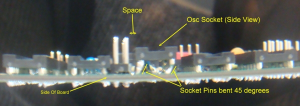
There is one complication with the CPU clock oscillator socket. Its actually too close to the wait state jumpers to fit the jumpers correctly (unless you use wire-wraps).  If you carefully bend the 4 pins of the socket to 45 degrees and solder it to the board this moves the socket and oscillator sufficiently away from the jumper pins so they can be inserted. Be sure you have 4 good solder joints. Here is a side picture of the board:-
  
 Side View 
  
Next insert all 5 LED's. Before soldering them in place ground the appropriate pin on the U66 socket to make sure it lights up.   I use blue for CPU active, green Halt, red EPROM select and yellow for wait states.

Next insert the LED bar (such as Jameco #2115531). Before soldering check the bars light up by grounding the appropriate pins on U67.
 
Check the voltage to sockets on the board is above 5V by placing the board in your S-100 system using an extender board. With no load you will typically get 5.00V  (+/- 0.25V).  BTW, your system should boot and run correctly with its Z80 master CPU board. If not, you have a serious solder bridge somewhere on the board.  Before you do anything else with a magnifying glass go over every socket on the board and examine for a proper solder joint. I like to "reheat" each joint just to be on the safe side. The silk screen/varnish on these boards us quite thick. It's easy not to have a good solder joint for the ground pins.  Double check.   Extra time here will save you hours later, (been there done that! ).

Here is a picture of the board at this stage:-
      
 Empty Board-2 
    
  
We will now build the board up in functional steps. Avoid the temptation of adding everything at once and popping it into your S-100 box. Step by step is faster in the end -- trust me.  We will set the board up configured as an S-100 bus slave.  Inputting port 0EDH (in my system, a Z80 monitor "W" or "O" command), will switch in this 80286 CPU board and switch out the Z80.

We will first add jumpers and IC's for this function.  While on jumpers, please note every time when we talk about jumpers,  position 1 is the square pad of the jumper. In order to minimize board trace lengths, its actual position/orientation on the board will differ from jumper to jumper.  Sometimes they are top to bottom or left to right, other times the exact opposite.  An incorrect jumper can be a real pain in debugging a non-working board. Check with the .brd schematic each time, to be sure . Make sure you correctly identify pin 2 in each case.

Jumper p36 1-2; P67 1-2 & 3-4 (both vertically); Add U92, U52, U89, U90, U91, U49.  Assuming we are using port 0EDH inputting data on this port with the bus Z80 CPU board will cause pin 1 of P36 to go high to low. Resetting the computer will bring it back high again.

Next we will install the HOLD/HLDA handshaking Circuit
Jumper p57 2-4 (horizontal); K12 1-2 (pin 1, RHS).  K9 4-5;  K10 3-4; JP12;  K4 1-2, P2 1-2, 3-4 (vertical), K2 1-2 (to use the oscillator as the CPU frequency source).   Later you can use  K2 2-3 if you want a crystal as the CPU frequency source.

For now insert an 8 MHz oscillator in socket P3.

Add U50, U53, U57, U59, U66, U63, U64 (the 82284 or 82C284, clock controller chip), U98 and U58.  Bend out U98 pin 1, ideally connect to pin 4. (Pin 1 should not be grounded).Place card in bus and activate. Pin 3 of U66 should go from tri-stated/inactive to high. The (blue) LED  D7 should light up.  Before activation in the bus the 4th from left bar (Halt) will light up. Upon activation the 4th bar should go out.
     
 Port Circuit-1
    

Next we will add the wait state circuit.
We will optimize the number of wait states later. With a 10MHz Crystal/Oscillator (5MHz S-100 bus clock), to be safe initially we will have 1 wait state for I/O cycles and 2 wait states for the on-board EEPROMS.   Here is how the jumpers should look:-
    
 Wait Jumpers
    
A maximum of 4 wait states can be added to I/O cycles or EEPROM access cycles on this board. Of course more can be added via external bus boards.  


Add U87 and U81.   Activate the board. Again the D7 led should light up.
 
Add the EPROM circuit.
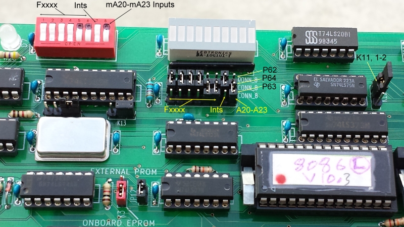
Unlike the 8086/8088, the 80286 starts upon reset at FFFFF0H in memory.  Its 4 high address lines (A20-A23) will be high. They will remain high until the CPU receives its first Far Jump.  At that point the address lines A20 -A23 will become active (and in real mode typically become 0's).  We need a way of recognizing this special A20-A23 high, situation.  U94 does this. If its pin 8  goes low, then U95 (a 2 line to 1 line selector)  forces mA20 - mA23 to 0's and via U73 the corresponding lines on the S-100 bus.  So an off-board EPROM board could be used with a standard 8086 monitor for example.  The onboard EEPROMs (containing our standard 8086 monitor code) are activated with the P62-P64 pin 8 jumper feeding pin 17 /SW3,8 of U80 (if K3 is jumpered 1-2).

Add U94,U95, U80, U72, U84, U85 and U86. Jumper K3 1-2.

Note should the 80286 address lines A20-A23 be anything other than FxxxxxH, U94 pin 8 is high. and U95 passes the address lines through directly from the CPU.

Address selection is obtained with U80 an 74LS682.  We use SW3 and Jumpers P62, P63 & P64 to select the EPROM address space

Please note, unlike our 8088 and 8086 boards, I use the full capacity of the two onboard 28C256 EEPROMS.  This means the address range of these EEPROMS will be from F0000H to FFFFFH.    This allows one to build a larger monitor adding things like for example the IBM-PC CGA Graphics Character set.   Be sure and set the equate 80286 = TRUE (and 8088 and 8086 = FALSE) in the monitor code. The code should start at position 0 within both EEPROMS. Low bytes in U82, high bytes in U83.

If you use 28C256 EEPROMS here is how the jumpers should look:-
  
 ROM Jumpers
  
 ROM Jumpers-2

BTW, you may note that the 80286 interrupt acknowledge signal is also factored into the equation.  This is to insure that should the 80286 send out an interrupt acknowledge signal, the U78 chip (see above) will transfer the interrupt vector down to the lower 8 bit data CPU input lines (via U63E and pin 3 of U52D).

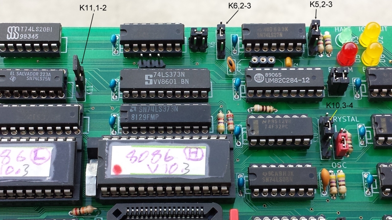
Continuing with our EPROM circuit; After adding U80 and Switch SW3,  jumper K3 1-2 (use onboard ROMS), and for 28C256's, jumpers K11 1-2, K5, 2-3 & K6 2-3.
Install U94, U95, U60 and U72.
Activate the board and check the D7 LED still lights up.

Install U84, U85 and U86.  Activate the board and check the D7 LED still lights up.  Here is a picture of the board at this stage.  If you are feeling lucky you can add the two 8086 Monitor EPROMS at this stage.  The Low byte PROM  always goes to the U82 socket. The high byte PROM goes to the U83 socket.
Here is a picture of the board at this stage.
          
 Prom Circuit Added-2
  
   
Add the DATA and ADDRESS Line circuits.

Add U76, U77, and U78.   Activate the board and check the D7 LED still lights up.
Add U55, U56. Add jumpers JP7, JP8. Activate the board and check the D7 LED still lights up.
Add address buffers U73, U74, U75.  Activate the board and check the D7 LED still lights up.

If you have the SMB and use the Z80 monitor "O" or "W" command to input from Port EDH (switch CPU's), the address displayed will actually be that location of the relevant code in the Z80 monitor itself.
Here is a picture of the board at this stage:-
    
 Address Circuit Added

  
Adding the 80286 CPU
Jumper K13 1-2.
Add U68 (82288 or 82C288), U1 and U67.  Add U71, U79, U74 and U2.  Add JP13 and JP14.
Activate the board and check the D7 LED still lights up. Also the HALT LED (green) D3 should light up.
 
Now comes the acid test, adding the 80286 CPU.  Carefully insert the CPU in U70. Insert in the bus and try transferring control to the 80286 CPU.   If you have a copy of the 8086 (or 80386) Monitor in your two ROMS the CPU should sign on and you are well on your way to getting your system going.

If the system hangs don't worry there are many options....


As a first test simply fill two EEPROMS with the 80286 instruction HALT (F4's).  Insert the two EPROMS in their sockets and activate the board. If all is well the CPU should after reset jump to memory location 0FFFF0H and activate the HALT LED (D3).  If so you are in good shape you can then proceed to build more elaborate EPROM based code as described above.

If you fail to force the CPU into a HALT state there may be something wrong with the board/CPU addressing capability.  One trick you can do is attach a jumper between P36 pin 2 and pin 2 of U58A.  Fill the EPROM with NOP's (90H). When the board is activated the CPU is immediately forced into a wait state. The address lines must show 0FFFF0H on your front panel if you are using for example our SMB. If not, something is wrong. Next switch your system into single step mode using the SMB. Only then, remove the pin2 of U58A jumper and single step the CPU.   The address lines should increase FFFF0, FFFF2,FFFF4,FFFF6... Check chips for these values.

This ability to single step the board in hardware is very useful for debugging.   I also have an option in the 8086 Monitor code at 0FFFF0H that if the IOBYTE port (0EFH) is 3FH (a switch on the SMB), the CPU will just continuously read that ports data and display the character on the console in a continuous non ending loop. 

Remember the default configuration for the 8086 monitor is for 16K of code to fit in the upper half of two 28C256 type EEPROMs.  (For the 8088 and 8086 boards using 28C256's,  you need to place the 16K  in the top half of the 32KX8 EEPROMs) This is not the case for this 80286 board. You can use the full 32K of each 28C256 EEPROM. You should set the "80286 Equate" in the 8086 monitor code to TRUE.  The code for the 80386 monitor always uses the full 28C256.

CPU SPEED
Using a 80386-12 AMD chip (12 MHz) I can get this board to boot CPM86 and MSDOS V4.01 using our 4MB Static RAM board @ 12MHz. (with no I/O or ROM wait states).  This requires the use of a 82C284-12 and at least an Intel 82288-10.  This is 2MHz above the Intel bus controller specs, your mileage may vary.

The board also works with our ROM/RAM board at that same speed and no wait states. 

With some older S100 Static RAM boards (particularly those that use PALs, such as the Godbout 128K static "RAM21" board or the BG Computers 256K Static RAM board), you need to bend out pin 2 of U56 and jumper it to pin 9 of U68 - the bus controller.  (Alternatively you can cut the trace going to pin 2 of U56 on the back of the board and add a short jumper to pin 9 of U68). This seems to provide the early MWRITE status signal these boards require.  Interestingly this is also the case for our 8088 CPU board (jumper K5,2-3),  but not the 8086 board

Source of Chips
For speeds of less than 10MHz on this board,  most chips can be 74LSxx. To get to 12MHz a number of these chips need to be replaced with 74Fxx or 74Sxx chips (see the schematic).  Particularly in this respect U78 and the chips that control it need to be 74Fxx chips.  This chip is the Achilles heel of the board where it swaps the high/low data lines for 8/16 bit access.  

I like to drive the S100 bus status lines (U55) with a 74F244 or better a 74S244.  However be aware if you are "messing around" with other boards in your system and have a bus conflict these drivers will often burn out a 74LSxx bus driver.  Input gates to the board should always be 74LSxx chips to avoid bus loading. BTW, U58A in the schematic should really be a 74LS21 for this reason.

The rated clock speed of the 80286, 82284 and 82288 is important.  For 12 MHz I use an AMD  80C286-12, an 82C284-12 and an Intel 82288-10 clock controller.  I could not find a 12MHz rated bus controller. Nevertheless on the two boards I have here, both run at 12MHz with no wait states.  The CPU and bus controller run warm but not red hot.

One excellent source of these chips is Unicorn Electronics.  I am looking for AMD 16 MHz chips illustrated here but have not found a source yet.


Configuring the 80286 as a Bus Master (No Slaves)

Up until now we have been using this board as an S-100 bus slave. Typically a Z80 CPU would control the bus until this board is activate by inputting from port EDH.  We will now convert the board to a true bus master where it initializes on power on/reset.  It's simple, just a few jumpers need to be changed.

First remove the current bus master (typically a Z80 board).
We then need to implement the boards Reset, Slave Reset and Power On Clear circuits IF these signals are not generated elsewhere on the S-100 bus.
If so Add jumpers JP4, JP5 and JP6
Jumper P57 1-3 (Bottom row horz.)
Jumper K9 2-4 and K10 2-4.
Insert the board in the bus. Power on, and/or hit the reset button, the monitor should come right up.
The only problem is the "Halt" LED stays on.  This is corrected by bending out pin 3 of U59A and adding back the jumper P57 2-4 (also leaving in place P57 1-3).


Configuring the 80286 as a Bus Master with Slave/DMA controllers

In this configuration the 80286 can pass control to another requesting bus controlling device if it follows the IEEE-969 protocol.   The trick is for the requesting slave device to raise the 80286 CPU Hold line, then when the 80286 is ready, it will raise its HLDA pin, this signals the slave device that a bus control transfer can occur.  Again a few more additional jumper changes are all that is required. 

First, unfortunately another small patch. If you have not already done so above, bend out U98 pin 1 and connect to pin 4. (Pin 1 should not be grounded).

I have tested this board configuration with our Master/Slave 68K board and our 6502 Master/Slave boards where they are both configured as bus slaves.   In both cases you can go back and forth between the two CPU's.

Configure the slave CPU (68K or 6502) so that inputting from port EDH activates the slave board.  First check you can activate the board with your Z80 board.

Remove the Z80 board and insert the 80286 board configured  as a bus master as described above.
Jumper K12 1-3, K9 3-4 and  K10 4-5
Add jumper JP11, JP18, K7 2-3 and K13 2-3.

From the monitor if you input from port ED control should switch over from the 80286 to the 68K (or 6502) monitor. 
Inputting again will switch control back to the 80286.  If this is done in code, the 80286 will always pick up where it left off.
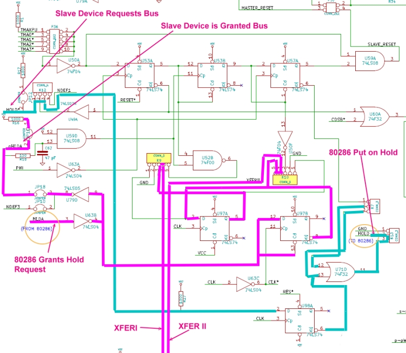
For those interested here is the path the signals take:-
 
   
 Schamatic 1
  
The slave requested HOLD* signal comes in to the board by jumpering K12 1-3. It is clocked by U98A and sent to the 80286 Hold Request pin as a high signal.  When the 80286 is ready to release the bus it will pass its high HLDA signal to pin 3 of U63A. This is sent back to the S-100 bus as a low pHLDA signal via U79D pin 8 (& JP18).   Seeing this signal low the slave device proceeds to take over the bus. On this 80286 board via U97B and U97A, first XFER II,  then XFER I are raised thereby inactivation the boards drivers to the bus (all status, control,  adders, data and CLK lines).  When this happens the 80286 is in a hold state and the S-100 slave device has complete control of the bus.  Once the slave device releases the bus (the exact reverse of the above process) the 80286 picks up exactly where it was -- as if nothing happened.


A Prototype V2 Version of the 80286 CPU S-100 Board.
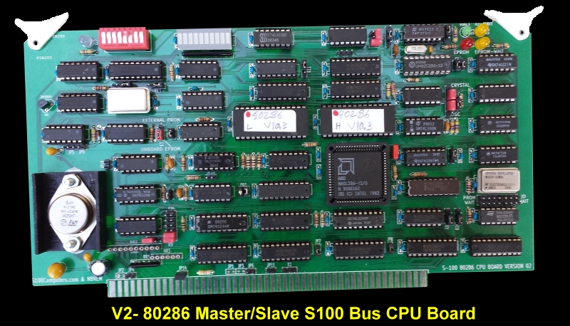
The above board has proven to be popular and reliable.  Over 20  boards were already made and distributed to users.  I decided to add a few small changes to the board to improve it's functionality. We are calling this board the V2-80286 CPU Board.

The changes/additions are:-
   
  1. Allow the use of older S100 bus static RAM boards to work with the board (see above), by adding jumpers for RAM read and write signals directly from the 82288 MWTC* and MRDC*. (jumpers K8 & K14)  
  2. Elaborate  on the above master /slave circuit so that the 80286 in slave mode can also pass control to a further "sub-slave" (or DMA controller) on the bus.  Patches described above for a master/slave configuration have now been corrected.
  3. Optimize the board layout and traces so the overall lengths are shorter and more reliable,
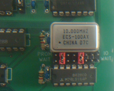
  4. Reposition the P3 Oscillator so it does not interfere with jumpers in P65 and p66 (see above).
  5. The halt LED light does not stay on in master mode.
  6. Reset jumper JP9 has been removed.  The master mode reset circuit was refined.
  7. Add and inactivate when in master mode S100 lines ADSB*, DDSB*, SDSB* and CDSB*.
          
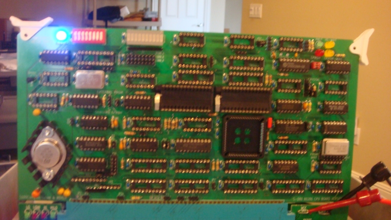
Here is a picture of the assembled V2 Prototype 80286 CPU board:-
    
 V2 Prototype 80286 Board
    
This new board retains all the chips and components of the original 80286 board,  (one extra 74LS32 chip was added). One can simply swap chips and utilized the new features of this board.  However be aware that some of the jumpers (and switch SW3 positions)  have changed.  The board with an AMD 80C286-16 CPU  I could get the board to run in my system with a 15MHz Oscillator "most of the time".  However I normally run the board with a 12 MHz AMD N80L286-12 (no I/O wait states), with on-board 28C256 EEPROMS or off-board EEPROMS on the MS-DOS support board.  At this speed the board is absolutely rock solid.

The main reason for building this V2 version was to expand its master slave capability (see below).   However by now allowing one to drive the S100 bus memory read/write signals from the 82288 I find that I can get the board to work reliably with many older S100 static RAM boards (For example the CompuPro RAM 21 Board).  This is accomplished by setting the jumpers of K8 & K14 to the 1-2 positions. In this position our own 4M static RAM and 1M RAM+ROM S100 boards also work fine.


Step By Step Building the V2 80286 CPU Board.
  Picture Of 80286 V2 Board 
 
The build instructions are fairly similar to the original (V1) board. However there are a few difference so I will repeat the whole write-up.
 
As always, first examine the bare board carefully for scratches or damaged traces, use a magnifying glass if need be. The quality of the boards we get is excellent. I must have done 50 by now, never had a problem, but there is always a first time. A broken trace is almost impossible to detect by eye on a completed board.  I find it useful to carefully slide a file at 45 degrees along the edges (front & back) of the S100 connectors for easier insertion into the bus. Carefully, just one or two strokes.
   
Next solder in all the required IC sockets, resistors, resistor arrays, capacitors, jumpers, and the voltage regulator.  Do not add the LED's or LED bar yet. Be sure you put the resistor arrays in with the correct orientation of pin 1. Check their values before  soldering (they are difficult to remove).  Remember if you already have 1K pull-up resistors for the  S-100 bus vector interrupt lines and DMA lines in your system (for example on your Z80 CPU board), you really don't need the resistors on this board  (RR2 & RR3).  You can insert single row sockets such as Jameco #78624 in case you want to add pull-up resistors in another system.  Be sure and insert the PLCC socket correctly with the notch at the top left-hand corner.  You might want to increase the value of R8 to ~200K Ohms if you have difficulties resetting some other boards in the system upon power on and you intend to run the board as a bus master.  This stretches out the reset, slave clear and POC pulses.
  
The TO-3 5V regulator heat sink must not touch the traces under it. Use either a mica TO-3 insulator or two small nut washers to separate it from the board itself.
  
For prototype boards I generally use "double swipe" IC sockets. For a critical board like this I prefer to use "Machine Tooled" IC sockets.  However they are more expensive and you have to be particularly careful not to bend the IC pins.  If you think you will be doing a lot of EEPROM burning you should use the Low Profile ZIF sockets (e.g. Jameco #102745) for the EEPROM socket.  If you think you will be changing the Monitor ROM's a lot you may want to consider two ZIF Test Sockets such as Jameco #103992.   If you use these sockets, do not insert caps C47 and C54. The two clock oscillators should have their own special sockets (e.g. Jameco #133006).  I in fact solder the 2MH oscillator directly to the board since it will never be changed. If not add it to the 2MHz socket.
 
Next insert all 5 LED's. Before soldering them in place ground the appropriate pin on the U66 socket to make sure it lights up.   I use blue for CPU active, green Halt, red EPROM select and yellow for wait states.  
There is one silk screen label error on the board. The text above the LED D3 ("Halt") is incorrect. It should be something like "80286 Active".  The actual HALT LED is D7.    You can use a green marker to cover the text.    For LED colors, I use Yellow for D6 & D2, Red for D5, Blue for D3 and green for D7.

Next insert the LED bar (such as Jameco #2115531). Before soldering check the bars light up by grounding the appropriate pins on U67.
 
Check the voltage to sockets on the board is above 5V by placing the board in your S-100 system using an extender board. With no load you will typically get 5.00V  (+/- 0.25V).  BTW, your system should boot and run correctly with its Z80 master CPU board. If not, you have a serious solder bridge somewhere on the board.  Before you do anything else with a magnifying glass go over every socket on the board and examine for a proper solder joint. I like to "reheat" each joint just to be on the safe side. The silk screen/varnish on these boards us quite thick. It's easy not to have a good solder joint for the ground pins.  Double check.   Extra time here will save you hours later, (been there done that! ).

We will now build the board up in functional steps. Avoid the temptation of adding everything at once and popping it into your S-100 box. Step by step is faster in the end -- trust me.  We will set the board up configured as an S-100 bus slave.  Inputting port 0EDH (in my system, a Z80 monitor "W" or "O" command), will switch in this 80286 CPU board and switch out the Z80.

We will first add jumpers and IC's for this function.  While on jumpers, please note every time when we talk about jumpers,  position 1 is the square pad of the jumper. In order to minimize board trace lengths, its actual position/orientation on the board will differ from jumper to jumper.  Sometimes they are top to bottom or left to right, other times the exact opposite.  An incorrect jumper can be a real pain in debugging a non-working board. Check with the .brd schematic each time, to be sure . Make sure you correctly identify pin 2 in each case.

Jumper p36 1-2; P67 1-2 & 3-4 (both vertically); Add U92, U52, U89, U90, U91, U49.  This P67 configuration assumes we are using port 0EDH. Inputting data on this port with the bus Z80 CPU board will cause pin 1 of P36 to go high to low. Resetting the computer will bring it back high again. 

Next we will install the HOLD/HLDA handshaking Circuit
Jumper p57 2-4 (vertical) and 5-6 (horizontal); K12 1-2 (pin 1, RHS).  K9 2-3 & 5-6;  K10 2-3 & 5-6; JP12;  K4 3-4 & 5-6, P2 1-2, 3-4 (vertical), K2 1-2 (to use the oscillator as the CPU frequency source).   Later you can use  K2 2-3 if you want a crystal as the CPU frequency source.

For now insert an 8 MHz oscillator in socket P3. Also while you are at it the 2MHz Oscillator.

Add U3, U50, U53, U57, U59, U66, U63, U64 (the 82284 or 82C284, clock controller chip), U98 and U58.  Place the card in the bus and activate. Pin 3 of U66 should go from tri-stated/inactive to high. The (blue) LED  D3 should light up.  Before activation in the bus the 4th from left bar (Halt) will light up. Upon activation the 4th bar should go out.  Here is a picture of the board at this stage:-
      
  V2 Board Switch
      
Next we will add the wait state circuit.
We will optimize the number of wait states later. With a 8MHz Crystal/Oscillator (4MHz S-100 bus clock), to be safe initially we will have 1 wait state for I/O cycles and 2 wait states for the on-board EEPROMS.   Here is how the jumpers should look:-
      
  V2 Board Wait Jumpers
      
A maximum of 4 wait states can be added to I/O cycles or EEPROM access cycles on this board. Of course more can be added via external bus boards.  


Add U87 and U81.   Activate the board. Again the D3 led should light up.

 
Add the EPROM circuit.
Unlike the 8086/8088, the 80286 starts upon reset at FFFFF0H in memory.  Its 4 high address lines (A20-A23) will be high. They will remain high until the CPU receives its first Far Jump.  At that point the address lines A20 -A23 will become active (and in real mode typically become 0's).  We need a way of recognizing this special A20-A23 high, situation.  U94 does this. If its pin 8  goes low, then U95 (a 2 line to 1 line selector)  forces mA20 - mA23 to 0's and via U73 the corresponding lines on the S-100 bus.  So an off-board EPROM board could be used with a standard 8086 monitor for example.  The onboard EEPROMs (containing our standard 8086 monitor code) are activated with the P62-P64 pin 8 jumper feeding pin 17 /SW3,8 of U80 (if K3 is jumpered 1-2).

Add U94,U95, U80, U72, U84, U85 and U86.

Note should the 80286 address lines A20-A23 be anything other than FxxxxxH, U94 pin 8 is high. and U95 passes the address lines through directly from the CPU.

Address selection is obtained with U80 an 74LS682.  We use SW3 to select the EPROM address space

Please note, unlike our 8088 and 8086 boards, I use the full capacity of the two onboard 28C256 EEPROMS.  This means the address range of these EEPROMS will be from F0000H to FFFFFH.    This allows one to build a larger monitor adding things like for example the IBM-PC CGA Graphics Character set.   Be sure and set the equate 80286 = TRUE (and 8088 and 8086 = FALSE) in the monitor code. The code should start at position 0 within both EEPROMS. Low bytes in U82, high bytes in U83.

If you use 28C256 EEPROMS here is how the jumpers should look:-
  
  V2 Board ROM Jumpers1
    

BTW, you may note that the 80286 interrupt acknowledge signal is also factored into the equation.  This is to insure that should the 80286 send out an interrupt acknowledge signal, the U78 chip (see above) will transfer the interrupt vector down to the lower 8 bit data CPU input lines (via U63E and pin 3 of U52D).

Continuing with our EPROM circuit; After adding U80 and Switch SW3,  jumper K3 1-2 (to use the onboard ROMS).  For 28C256's, jumpers K11 1-2, K5, 2-3 & K6 2-3.
Install U94, U95, U60 and U72.
Activate the board and check the D3 LED still lights up.

Here is a picture of the board at this stage.  If you are feeling lucky you can add the two 8086 Monitor EPROMS at this stage.  The Low byte PROM  always goes to the U82 socket. The high byte PROM goes to the U83 socket.
Here is a picture of the board at this stage.
             
  V2 Board ROM Jumpers2
    
   
Add the DATA and ADDRESS Line circuits.

Add U76, U77, and U78.   Activate the board and check the D3 LED still lights up.
Add U55, U56. Add jumpers JP7, JP8. Activate the board and check the D3 LED still lights up.
Add address buffers U73, U74, U75.  Activate the board and check the D3 LED still lights up.

If you have the SMB and use the Z80 monitor "O" or "W" command to input from Port EDH (switch CPU's), the address displayed will actually be that location of the relevant code in the Z80 monitor itself.
Here is a picture of the board at this stage:-
      
  V2 Board before CPU

     
Adding the 80286 CPU
Jumper K13 1-2. Jumper  JP7 & JP8 if your system front panel does not generate these signals.
Add U68 (a 82288 or 82C288), U1 and U67.  Add U71, U58, U60, and U2.  Add JP13 and JP14 if there are no other boards pulling these lines high.
Activate the board and check the D3 LED still lights up. Also the HALT LED (green) D7 should light up.
 
Now comes the acid test, adding the 80286 CPU.  Carefully insert the CPU in U70. Insert in the bus and try transferring control to the 80286 CPU.   If you have a copy of the 8086 (or 80386) Monitor in your two ROMS the CPU should sign on and you are well on your way to getting your system going.

If the system hangs don't worry there are many options....


As a first test simply fill two EEPROMS with the 80286 instruction HALT (F4's).  Insert the two EPROMS in their sockets and activate the board. If all is well the CPU should after reset jump to memory location 0FFFF0H and activate the HALT LED (D7).  If so you are in good shape you can then proceed to build more elaborate EPROM based code as described above.

If you fail to force the CPU into a HALT state there may be something wrong with the board/CPU addressing capability.  One trick you can do is attach a jumper between P36 pin 2 and pin 2 of U58A.  Fill the EPROM with NOP's (90H). When the board is activated the CPU is immediately forced into a wait state. The address lines must show 0FFFF0H on your front panel if you are using for example our SMB. If not, something is wrong. Next switch your system into single step mode using the SMB. Only then, remove the pin2 of U58A jumper and single step the CPU.   The address lines should increase FFFF0, FFFF2,FFFF4,FFFF6... Check chips for these values.

This ability to single step the board in hardware is very useful for debugging.   I also have an option in the 8086 Monitor code at 0FFFF0H that if the IOBYTE port (0EFH) is 3FH (a switch on the SMB), the CPU will just continuously read that ports data and display the character on the console in a continuous non ending loop. 

Remember the default configuration for the 8086 monitor is for 16K of code to fit in the upper half of two 28C256 type EEPROMs.  (For the 8088 and 8086 boards using 28C256's,  you need to place the 16K  in the top half of the 32KX8 EEPROMs) This is not the case for this 80286 board. You can use the full 32K of each 28C256 EEPROM. You should set the "80286 Equate" in the 8086 monitor code to TRUE.  The code for the 80386 monitor always uses the full 28C256.

Also remember that while the SMB will display the correct address on the bus in single step mode the data displayed will not be correct IF you are using the onboard EPROMS. To see the actual data you need to use off-board ROMs' such as those on our MSDOS support board or RAM+ROM board. 

Once you have a working system you can play around with the crystal or oscillator frequency.   In the extender card at 12MHz I use one EPROM wait state and one I/O wait state. In the bus itself only one I/O wait state seems to be required -- your mileage may vary.  I have not succeed in reliably getting higher speeds with this board (even using an AMD N80C286-16). However this may be because I cannot find a 16 MHz 82284 and 82286.
While not really necessary in slave mode, you can add jumpers JP9, JP16, JP17, JP19 & JP15.  Also you can add a crystal (X1) instead of an oscillator. In that case K2 needs to be jumpered K2-3.


The V2-80286 as an S100 Bus Slave.
This is by far the most common configuration for this board and is how we have the above build board configured.  In such a system typically a Z80 CPU would control the bus until this board is activated by one of the TMA0-3 S-100 lines.    This can be accomplished by either inputting data from the boards on-board I/O port 0EDH, or utilizing our SMB board to do so.  It is very important that all the correct jumpers of the board be correct for this to happen.
           
 
Jumper   Function 
JP4,JP5,JP6Used only if the board is to act as a bus master.  Generates Power On reset etc.  (Normally open)
JP12Use only if no other board on the bus pulls up the S-100 HOLD signal  (Normally open)
JP11Use only if no other board on the bus pulls up the S-100 HLDA signal  (Normally open)
K11This forces the 80286 reset address FFFFF0 to 0FFFF0 so the 8086 and 80286 external ROMS can be used in the same bus. Normally 1-2.
JP7Use only if no other board generates the S-100 2MHz clock signal when the 80286 is active (Closed in my system)
JP8 Use only if no other board generates the S-100 MWRT signal when the 80286 is active (Closed in my system)
P65Sets number of wait states for onboard EEPROM (0-4). (Open, I use 1 wait state with 28C256 EEPROMS at 12MHz)
P66Sets number of wait states for bus I/O and INTA cycles (0-4). I use 1 wait state in my system at 12MHz.
(Slow boards generate their own wait states)
P57Set to slave mode, so 5-6 and 4-2
P36Determines what S100 TMA line activates this board.  (Normally TMA0* from SMB, so P26 3-4. For onboard activation use 1-2 & 3-4) 
K8 Normally 1-2. MWTC* from 82288. Position 2-3 does not seem to work with some older S100 static RAM boards
K14Normally 1-2. MRDC* from 82288.  Position 2-3 does not seem to work with some older S100 static RAM boards
P13, P14Use only if no other board on the bus pulls up these signals  (Open in my system)
K1Brings the 80286 BHE signal to the bus for experimental purposes  (Normally open)
K21-2, Oscillator supplies CPU clock  (4-12MHz).   2-3 Onboard crystal supplies clock  (4-12 MHz)     (Normally 1-2)
K3Normally 1-2. If set 2-3 the onboard EEPROM circuit is invisible to the 80286. Use the latter if using ROMS for example on the MSDOS support board.
K5, K6These pins must be carefully selected for different EEPROM and EPROM types         (For 28C256's,  K5 2-3, K6 2-3)
K4Determines when the 80286 LEDs are enabled.   (Normally 5-6 & 3-4)
P67 Normally 1-2 and 3-4. This selects the port to activate the 80286 board on the bus, port EDH
SW3This selects where the onboard EEPROMS will reside in the CPU's 1MG address space
Normally 28C256 ROMs will be at FF000H, so SW3 will be open, open, open, open, closed, closed, open, open
RR2, RR3Insert a 1K resistor network in these positions IF no other board on the bus pulls VI0* - VI7* etc. high.  Normally they are not jumpered (they are pulled up by the Z80 master CPU).  It is essential multiple boards do not pull them high.
K9Determines when/how the XFER-I  process takes place  (For Slave mode 2-3 and 5-6)
K10Determines when/how the XFER-II process takes place   (For slave mode 2-3 and 4-5)
JP10 & JP18 Open in slave mode
K12 Send HOLD* request back to master (Z80), so K12 1-2
K7 & K13Used to put 80286 in hold state when high. Here, K7 2-3 and K13, 1-2
JP1,JP2 & JP3  If you S-100 bus is IEEE-696 compatible these jumpers allow extra ground access to the board. Most S-100 busses don't have this installed 
JP9,JP16,PP17,
JP19 & JP15 
These jumpers allow the board to disable the address, data, status and data lines. Not really relevant here but can be jumpered 
      
The circuit (see below) to carry out the "hand shake" controlled switching between the two CPU's is more or less as described above for the (V1) 80286 board.  The circuit is a little more complex and is shown here:-
      
  V2 FINAL circuit 1

The slave request is intimated by lowering pin 1 of U50A. This one clock cycle later lowers the S100 bus line HOLD* (K12 pin 1 goes low).  Pin 4 of U52B is also pulled low.  The Z80 master recognizes a DMA request, inactivates its Address, Data and Status lines and raises pHLDA.  This raises pin 5 of U52A (via U59D). Pin 6 of U52A is then lowered which lowers the  XFER-I line on the board.   This Activates U55 is for a brief moment both CPU are driving pSync, pWR*, pDBIN and pSTVAL*.  (The 10 Ohm resistors from U55 are there to make sure the drivers don't overheat).  On the next S100 clock cycle the Z80 inactivates its pSync, pWR*, pDBIN and pSTVAL* lines.  At exactly the same time pin 12 of U50F goes low via the clocking of U53B. This lowers pin 4 & 5 of K10 and eventually the boards XFER-II line.   XFER-II activates the 80286 Address, Data and Status lines and completes the transfer of control of the 80286 to the S100 bus.

Here is a close-up pair of pictures with the above jumper arrangements:-
   
  V2 Slave Jumpers 1
  
  V2 Slave Jumpers 2


The V2-80286 as an S100 Bus Master (No Slaves or DMA requests).
This is in fact the simplest board configuration. When the 80286 board comes on after power up (or after a hardware reset), the 80286 will completely control the S100 bus.  Depending on the system motherboard and/or front panel the S100 reset* signal (pin 76) , slave clear* (pin 54) and POC* (pin 99) may or may need to be generated. If not, they need to be generated on this 80286 board. Here are the main difference is the jumper configurations from those described above.
         
 
Jumper   Function 
JP4,JP5,JP6 Used if the board is to act as a bus master and the relevant signals are not generated elsewhere in the system.  (In my system, normally open)
With some older boards POC* should return high before Reset*.  May want to use only JP4 and JP5
P57Set to master mode, so 1-3 only
K9Pins 2,3 and 5 are connected (ground) to insure XFER-I will always be low
K10Pins 2,3 and 5 are connected (ground) to insure XFER-II will always be low

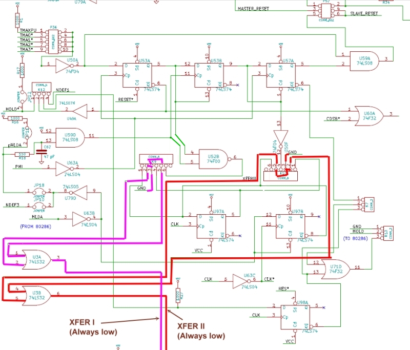
The circuit is quite simple and is shown here:-
  
  V2 FINAL Circuit 2
  
All we have to do is insure that the XFER-I and XFER-II lines remain low and that the reset line going to pin 11 of the 82284 (U64), is high.


Configuring the 80286 as a Bus Master with Slave/DMA controllers
In this configuration the 80286 can pass control to another requesting bus controlling device if it follows the IEEE-969 protocol.   The trick is for the requesting slave device to raise the 80286 CPU Hold line, then when the 80286 is ready, it will raise its HLDA pin, this signals the slave device that a bus control transfer can occur.  The minor errors/changes for the original "V1" board have now been corrected.
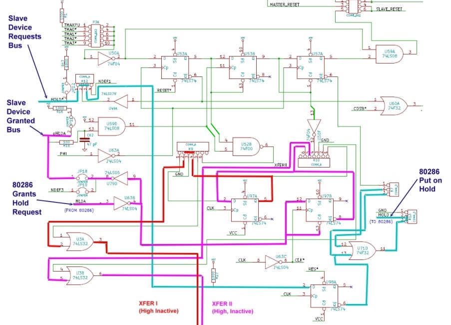
Here is the new circuit layout:-
  
  V2 FINAL Circuit 3a
  
The slave requested HOLD* signal comes in to the board by jumpering K12 1-3. It is clocked by U98A and sent to the 80286 Hold Request pin as a high signal (K13, 2-3).  When the 80286 is ready to release the bus it will pass its high HLDA signal to pin 3 of U63A. This is sent back to the S-100 bus as a low pHLDA signal via U79D pin 8 (& JP18).   Seeing this signal low, the slave device proceeds to take over the bus. On this 80286 board via U97B and U97A, first XFER II,  then XFER I are raised thereby inactivation the boards drivers to the bus (all status, control,  adders, data and CLK lines).  When this happens the 80286 is in a hold state and the S-100 slave device has complete control of the bus.  Once the slave device releases the bus (the exact reverse of the above process) the 80286 picks up exactly where it was -- as if nothing happened.
 
 
Jumper   Function 
JP4,JP5,JP6 Used if the board is to act as a bus master and the relevant signals are not generated elsewhere in the system.  (In my system, normally open)
With some older boards POC* should return high before Reset*.  May want to use only JP4 and JP5
P57Set to master mode, so 1-3 only
K12Need to input a DMA request from another board.  So K12 is set 1-3.
K13, K7We need to allow the 80286 to grant a hold state. So K13 2-3 and K7 2-3
JP18Add jumper. This places the 80286 Hold acknowledge signal (pHLDA) on the bus letting the requesting slave know it is ready for a bus transfer.
K9Pins 2-4, and 3-5 are connected to insure XFER-I will go HIGH when the slave has control of the bus
K10Pins 2-3 and 5-6 are connected (ground) to insure XFER-II will go HIGH when the slave has control of the bus
  
We can demonstrate this process by having the 80286 board come up as a bus master and also have in the bus our 68010 CPU board as a bus slave.   The 68010 board is activated by lowering TMA0*. That board will then trigger HOLD* on this board, wait for pHLDA to be returned to it and then take control of the bus.

Here is a short video demonstrating this process:-


Please see here for more information on software to run with this board.


The Z80 CPU board as a Bus Master, the V2-80286 as an S100 Bus Slave with the ability to call a "sub-slave".
This is a fairly complex arrangement  and probably will only be used by a few people. Nevertheless it illustrates the flexibility of these boards and the S100 bus. It should be noted that while the IEEE-696 S-100 specs defined one bus master and up to 16 bus slaves, in all cases the bus master always called the slave CPU's or DMA controller. The specs were undefined for example how a slave CPU would do DMA.   It was always anticipate control would be passed back to the bus master and that master would handle the DMA request.   While feasible (though I have not seen it done), I felt that by adding a few more jumpers and utilizing the S100 bus undefined lines NDEF1 and NDEF3 we can drop DMA control one level further down.  Thereby eliminating the software need for the master CPU to handle DMA requests.
 
As I just said above, we will need to use two unassigned S-100 bus lines for transfer control. We will use a lowered NDEF1 (S100 pin 21) as the line to request a DMA transfer control from the (slave) 80286 board.  The sub-slave/DMA controller will acknowledge it is ready the receive control by lowering NDEF3 (S100 pin 66).  It goes without saying,  any slave S100 board will have to have jumpers on board to recognize these lines as equivalent to the S100 bus signals  HOLD* and pHLDA.

Here is the layout:-
 
  V2 FINAL Circuit 4

Here is a summary or the relevant jumper configurations:-
  
 
Jumper   Function 
JP4,JP5,JP6 Used if the board is to act as a bus master and the relevant signals are not generated elsewhere in the system.  (In my system, normally open)
With some older boards POC* should return high before Reset*.  May want to use only JP4 and JP5
P57Set to slave mode, so 5-6 and 4-2
K12Need to input a DMA request from another board.  So K12 is set 1-3 and K12 3-4
K13, K7We need to allow the 80286 to grant a hold state. So K13 2-3 and K7 1-2
JP10Add jumper. (Make sure JP 18 is open). This signals to this slave 80286 that the sub-slave controller it is ready for a bus transfer.
K9Pins 5-6, and 2-4 are connected to insure XFER-I will go HIGH when the sub-slave has control of the bus
K10Pins 4-5 and 2-6 are connected to insure XFER-II will go HIGH when the sub-slave has control of the bus
 
In "normal" 80286 slave mode, the circuit behaves as described above.  When we want to transfer control one level further down we must inactivate XFER-I and XFER-II driven drivers. We cannot wind things back as for a slave transfer back to the master. Instead we inactivate them by raising pins 3 and 6 of U3 (see above).   However again we have to do it is a step by step clockwork process in conjunction with the sub-slave CPU (or DMA controller) that will be utilizing the bus. 

Two further points; The order of giving up the bus drivers is the reverse as that for a slave, (as far as the sub-slave is concerned, this board is a bus master).  So we inactivate XFER-II first and one clock cycle later XFER-I.    Second we cannot use the usual handshake signals HOLD* and pHLDA since these are already in use.   We will utilize two of the S-100 bus unassigned signal lines, NDEF1 and NDEF3 (pins 22 & 67) for this purpose.  There is no way around this requirement.  On all future slave CPU boards I will add a jumper to utilize these lines.  Fortunately our 68000 CPU master/slave board has the NDEF 1 & 3 pins as jumpers on board.   In the example video below I jumpered the 68K board JP7 pin to its JP 5 pin 2.  I had to bend out pin 10 of its U70 and connect it to pin 2 of its JP2. Make sure the 68K JP 7 jumper is not connected.
  
Here is a short video demonstrating this double level master, slave, slave process using the prototype version of this board:-


Please note that this process is relatively complex. It's best to step your board configuration along.
First setup the 80286 as a bus slave. Show you can transfer control to it.
Next setup your 68000/68010 board as a slave. Show you can transfer control to it.
Using two different TMA lines (TMA0* & TMA1*). Show you can from the Z80 bring up either of the CPU's. In each case going back to the Z80.
Only then should you configure the board as described above.

Bugs.
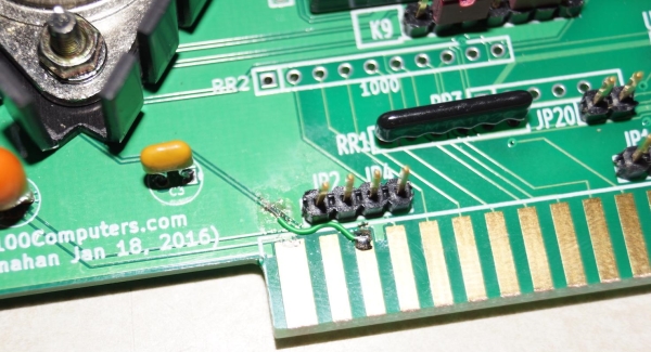
Alex Swedenburg has noticed an etching problem with the XRDY line going to pin 3 on the S100 bus.  There seems to be a short to ground in the area. it's impossible to see as the whole area is covered with the silkscreen. Check if pin 4 of U58 is shorted to ground on the new board.  If so cut and rejoin the trace as shown in this picture.  This error appears on the V2a boards only. The V2 boards appear to be fine.
     
  XRDY Error
    
No other bugs have been reported for these board currently.  However remember if you are using the onboard port (EDH) to activate the board be sure you jumper P36 1-2 & 3-4.  This is because other boards may be expecting the TMA0* line to be low when this board is active.   The onboard port alone will not lower the TMA0* line. 

S100 Bus Master/Slaves.
Please note this board is normally set to act as an IEEE-696 bus slave.  It should work with our Z80 CPU board described on this site. It is important to remember however that this 80286 CPU board is counting on the fact that when the bus master to relinquishes control of the bus to a slave device, the bus master inactivates all of its address, data, status and control lines while the slave has control of the bus. The S100 bus signals ADSB*, DDSB*, SDSB* and CDSB* are expected to all go low as specified by the IEEE-696 protocol.  Some older S100 bus Z80 boards driven boards may not do this.

This board can configured as a stand alone bus master. However you have to configure it as described above to lower the S100 bus signals ADSB*, DDSB*, SDSB* and CDSB* once control is transferred to the slave.

Source of Chips
For the CPU & support chips
I prefer the CMOS versions rather than the original older TTL versions which tend to run hot.   I use Unicorn Electronics as a source, but there are others -- even eBay. Be sure you get the 82C2xx chips and not the 82Cxx chips. The latter are support chips for the 8086 CPU.

A Production Board
Realizing that a number of people might want to utilize a board like this together with a group of people on the  Google Groups S100Computers Forum, "group purchases" are made from time to time. Please see here for more information.

The links below will contain the most recent schematic of this board.
Note, it may change over time and some IC part or pin numbers may not correlate exactly with the text in the article above.

MOST CURRENT 80286 CPU BOARD SCHEMATIC  (V1, FINAL-6, 3/18/2014)
MOST CURRENT 80286 CPU  BOARD LAYOUT  (V1, FINAL-6, 3/18/2014)
LIST OF BOARD ITEMS  (V3, FINAL-6 PRODUCTION RUN, 11/19/2013)


FINAL PROTOTYPE V2- 80286 CPU BOARD SCHEMATIC  (V2, 4/22/2014)
FINAL PROTOTYPE V2- 80286 CPU  BOARD LAYOUT  (V2, 4/22/2014)
Most current KiCAD files for this board  (S100 80286 V2.zip  11/5/2014)


Other pages describing my S-100 hardware and software.
Please click here to continue...

This page was last modified on 11/30/2017