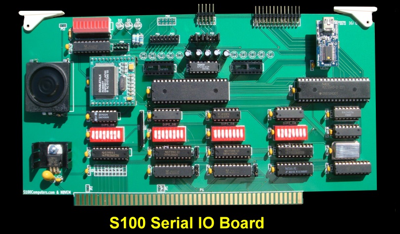
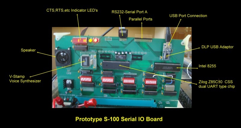
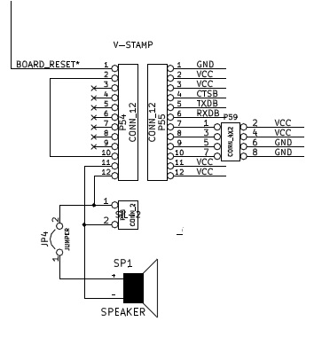
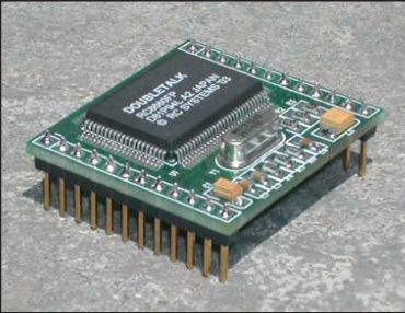
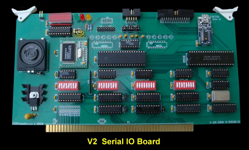
Serial IO Board Version V3.1
The demand for this board has been quite large. A
third version of this board was laid out. This version is called V3.1. The
first batch was made by PCBCart in Jan 2016. It is
identical to the above V2 board except that a
more detailed Silkscreen was drawn up. This one has labels over all the
IC's, and better legends over the switches and connectors.
The KiCAD and related files are presented below.
BUGS V3.1
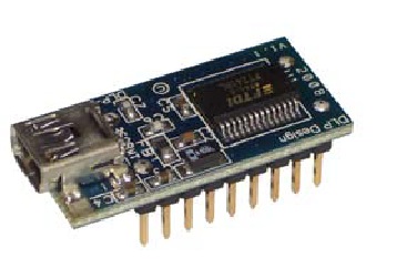
Wayne Warthen, pointed out that the default EEPROM mode for the newer
USB1232H "chip" is set for a mode other than
FIFO. This requires the board to be re-programmed using FTDIs tool
T_Prog utility
(http://www.ftdichip.com/Support/Utilities.htm#FT_Prog) to
make the FIFO mode work as described above. The older USB245R
"chip" does not require this modification and works as described
above.
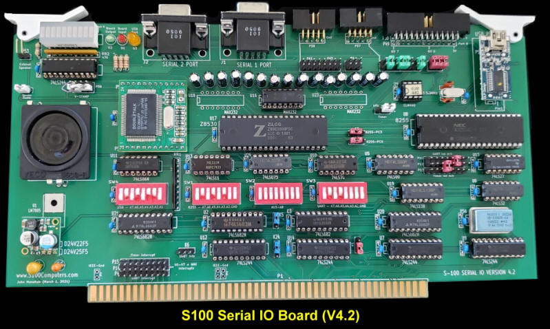
Serial IO Board Version V4.2
This board has been around 2010. It has shown itself to
be very popular and reliable. It is overdue a few tweaks and
improvements however.
Damian Wildie in Australia has
utilized the board as a console serial interface for use with Cromemco's
Cromix using our 68030 CPU
board.
Cromix is a popular OS for Cromemco computers with its
Unix like structure.
Please see:-
Introduction to Cromix-Plus Users Manual.pdf
Cromix-Plus Programmers Reference Manual.pdf
for more
information.
The new V4.2 board is identical to the V3.1 board with the following
additions:-
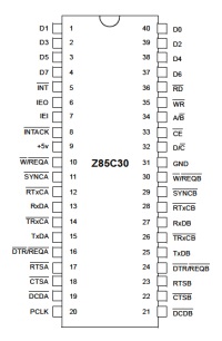
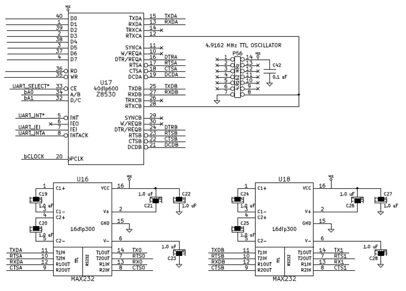
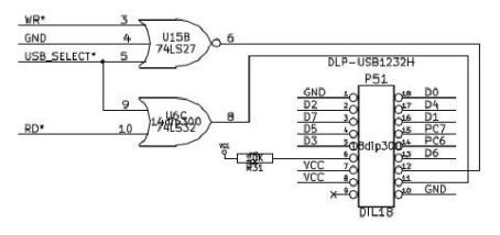
Z8530 Interrupts
The TBE & RDA interrupts generated by the Z8530 (U17) for both serial
ports are needed to run Cromix. Configuring the Z8530 to trigger
INT
is fairly straight forward, however,
the Z8530 requires its
INTACK
pin to be pulled low to deassert the
INT
signal. There is no circuitry on the board V3.1 board to do this.
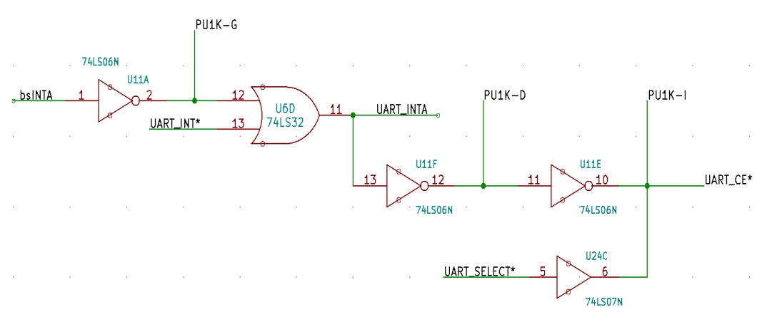
Damian implemented the following circuit using the spare gates and pull-ups
on the V3.1 board to do this.
bsINTA
is the S100
sINTA
via the spare buffer in U14. We have now incorporated a
proper
INTACK
signal in the V4.2 board.
An Onboard Timer Signal
The
Cromemco DPU &
XPU
CPU boards do not have a RTC chip. They rely on two timer
interrupts from the TMS5501 on the
16FDC
and 64FDC Boards.
One interrupt at 16 ms intervals for the system clock and another at 524288
uS for the real time clock. These values are not critical, A single
~100ms SMB board interrupt
for the system clock and from this calculating the real time increment
can be done -- but is not real accurate and subject to drift.
At boot time, the user is required to enter the current data and time to
initialize the real time clock. A stable 60Hz interrupt would work much
better. If this interrupt was to be combined with the Z8530's
interrupt, it would be necessary to be able to quickly identify the source.
Alternatively a different interrupt level could be used. It is
possible to utilize the timer on our
MSDOS Support Board but
this adds another board to the minimum system to run Cromix. A better
solution is to add an
EML440 timer
chip to the serial board. We have had good success with this chip on our
PDP11 CPU board.
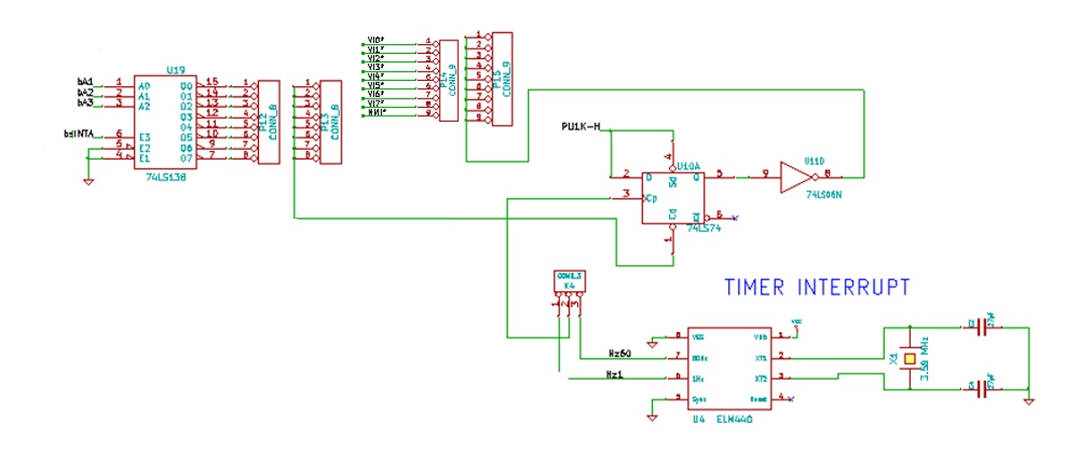
With at 60Hz with a 50% duty cycle from the ELM440, the Z8530 interrupts are
frequently being missed. By changing the square wave to a 10uS pulse
however it works reliably. Damian used a level 3 for the timer and 5 for
the Z8530. With this arrangement the interrupt circuitry on the 68030 board
appears to be working correctly, the 74LS148 correctly prioritized the level
5 interrupt whilst the level 3 line is held low. The timer interrupt
handler does not explicitly mask higher level interrupts, unless there is
something in Cromix that does. To work around this, he added a
resettable D type flip-flop to the output of the ELM440 that is reset by the
S100 bus sINTA signal. Here is the
relevant part of the schematic:-
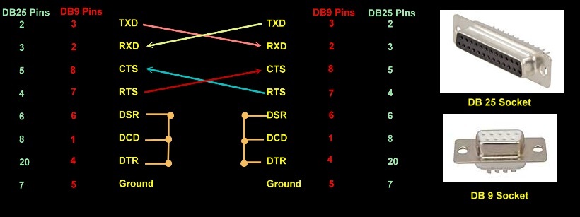
DB9 Connectors
The original Serial Board has a fair amount of unused board space.
It utilized two 10 pin headers to connect ribbon cables to the back of the
S100 Box for serial connections. For convenience we now add two female
DB9 sockets to the top of the board for simple quick connections. In
most cases this of course will not allow the cover to be placed on the top
of the S100 box however. Something in reality rarely done!
Pololu 5V Voltage Regulators
Besides the footprint for the linear 5V regulator and space for a heat sink
the V4.2 board now has pads to utilize the Pololu
D24V22F5 or
D24V25F5 5V regulators as well.
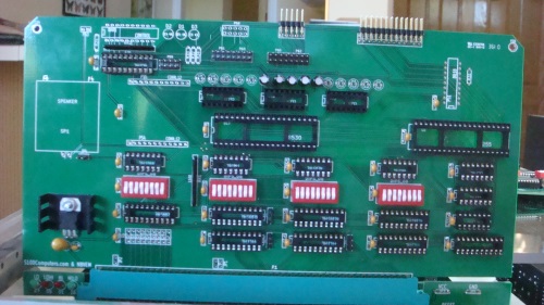
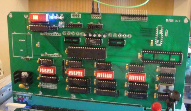
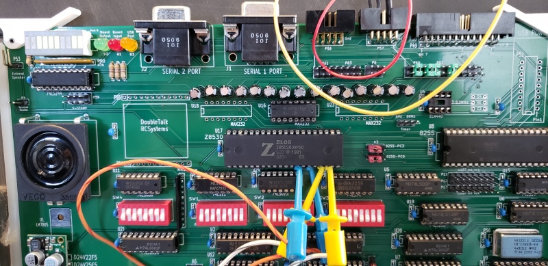
Here is a picture of this Serial IO board V4.2 version.
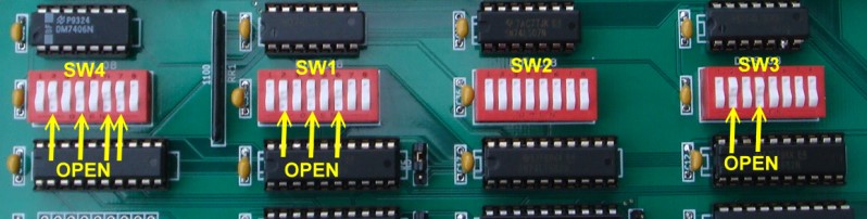
The build process and jumper connections for this board are almost identical
to that of the V3.1 version. The configuration switch settings are
identical.
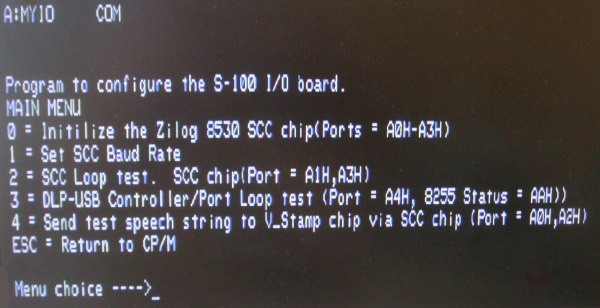
During the build be sure you get the serial "loop back" test
working before going further. If you pass that test much of the board is
working. Use the MYIO.Z80 program to test
the board.
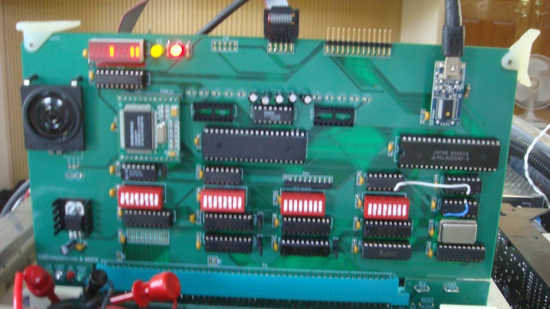
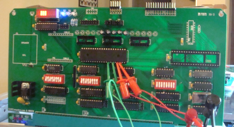
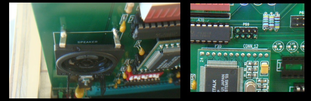
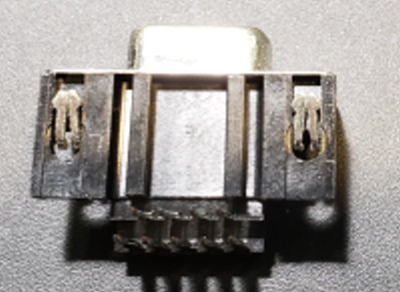
Here again is a close-up picture:-
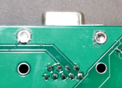
Please note for some DB9 Sockets the large ground/case pins do not line up
with the large board holes. Just bend them flat and later fill the two
board holes with solder. This attaches them to the board.
Here is a picture:-
Setting up jumpers/wires for an RS232 connection makes one really appreciate
the USB socket. The board has jumpers such that almost any
configuration can be configured. That's the good news. The bad news is
that are many possible connections to chose from. You first need to
decide if your serial connection is a "modem" or a "Computer" to another
terminal/computer. This affects how the RS232 pins 2 and 3 are
configured.
I use this board a lot to download and upload programs to/from my PC.
For this I use a USB port on the PC and a Serial -> USB port adaptor
connection on this board that connects in to the boards Serial port #1.
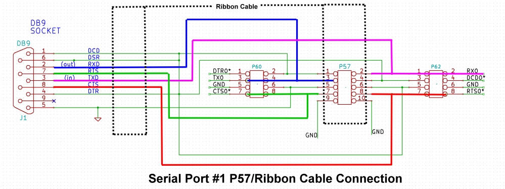
For the onboard P57 socket connected to a ribbon cable that is connected to
a DB9 female socket at the back of the S100 Box here is the jumper
arrangement.
The ribbon cable P57 pins connect to the DB9 pins as follows.
Cable
1->DB9 1, Cable 2->DB9 3, Cable 3->DB9 2,
Cable 4->DB9 4, Cable 5->DB9 5
Cable 6->DB9 4+6+1, cable 7->DB9 7, Cable 8->DB9 8, Cable 9->DB9 9,
Cable 10->DB9 NC.
P60 3->4, 7->8. and for P62 1->2, 7->8
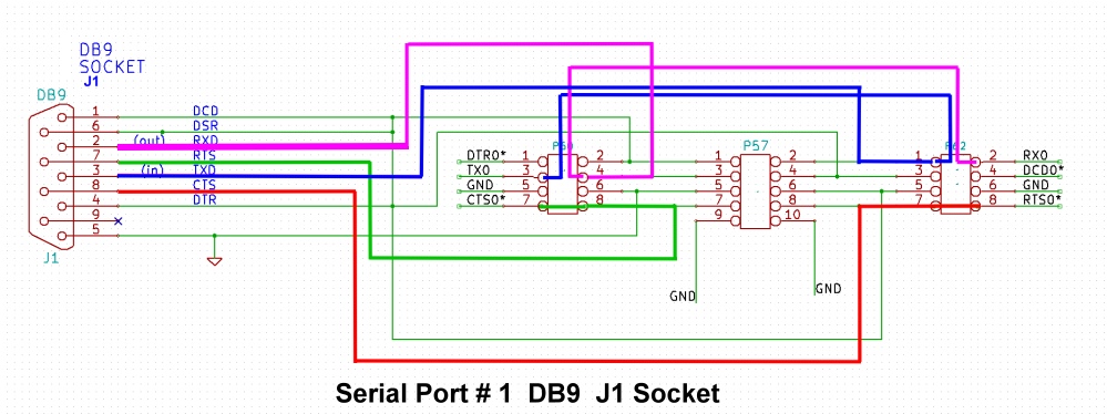
If you use the onboard DB9 J1 socket, here is the setup:-
P60 pin 3 to P62 pin 1, and P62 pin 1 to P60 pin 4.
Also P60 7->8 and P62 7->8.
Jumper P5 1->2, 3->4, 5->6.
The
ELM440 (U4 )can be ordered directly from ELM
here (in Canada). Its not
cheap ($8 each), but it seems very reliable/accurate. Here is the
ELM440 datasheet.
It
should provied a 1 or 60Hz signal on K4 and can be used as described above
or as a rough RTC.
Bugs
Henry Broekhuyse and Damian Wildie pointed out there
are errors affecting serial port 1 connector J1 and
J2 connector for serial port 2.
The schematic shows DB9B_RxD connecting J2-2 to P63-1 and P58-2. On the
board, DB9B_RxD is actually connected to P63-3 and P58-4
The schematic shows DB9B_DTR connecting J2-4 to P61-2 and P58-1. On the
board, DB9B_DTR is actually connected to P61-6 and P58-5
The schematic shows DB9A_DTR connecting J1-4 to P60-2 and P57-1. On the
board, DB9A_DTR is actually connected to P60-6 and P57-5