S100 Computers

HomeS-100 Boards HistoryNew BoardsSoftwareBoards For Sale
ForumOther Web SitesNewsIndex  

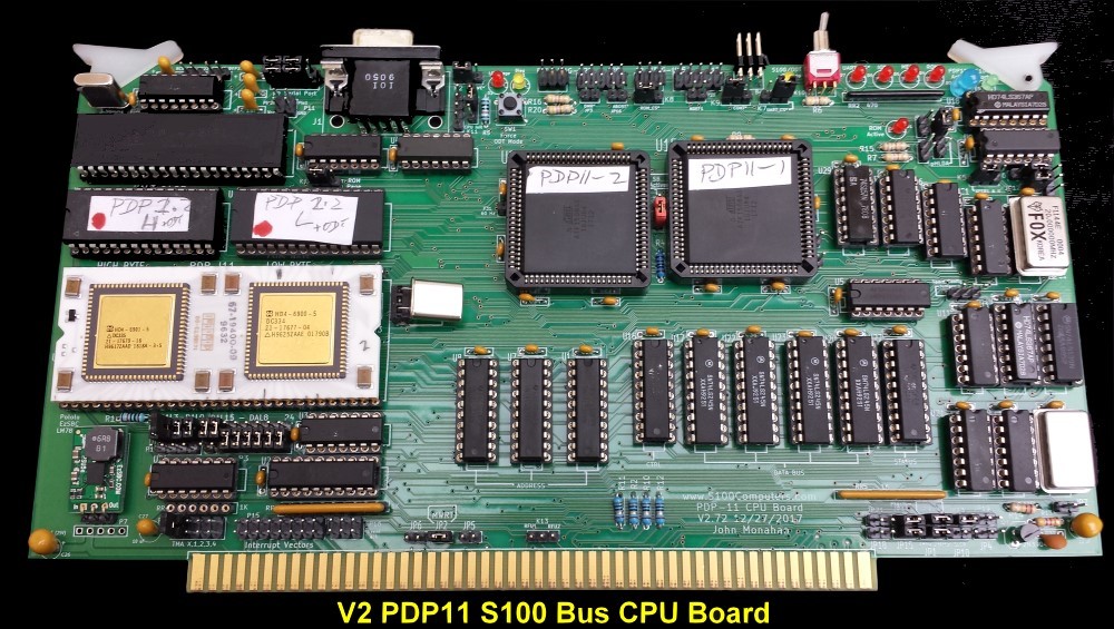
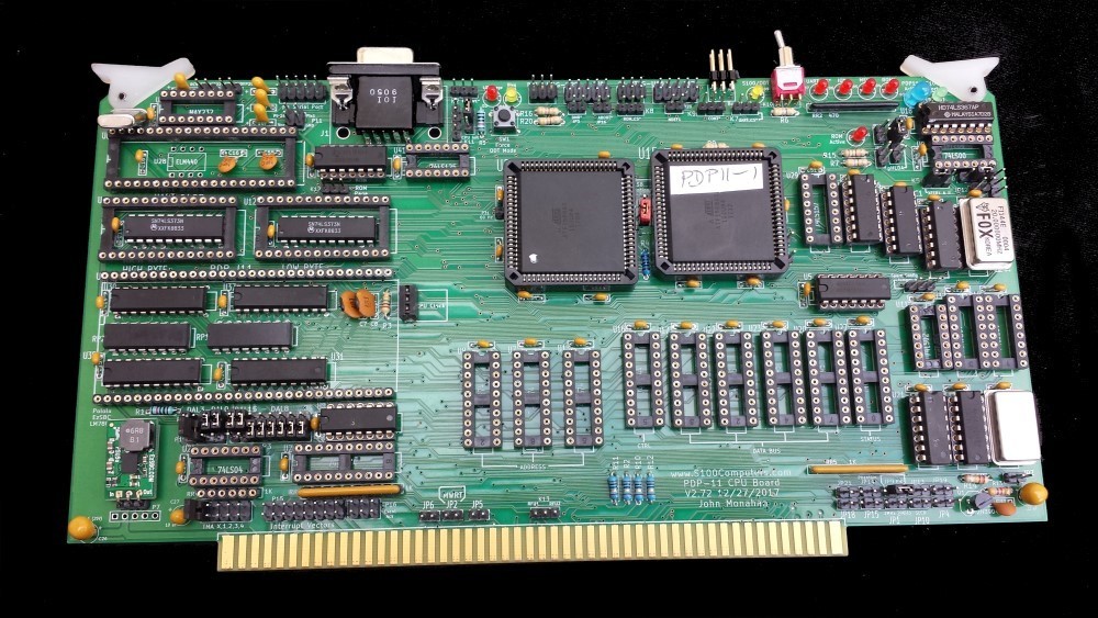
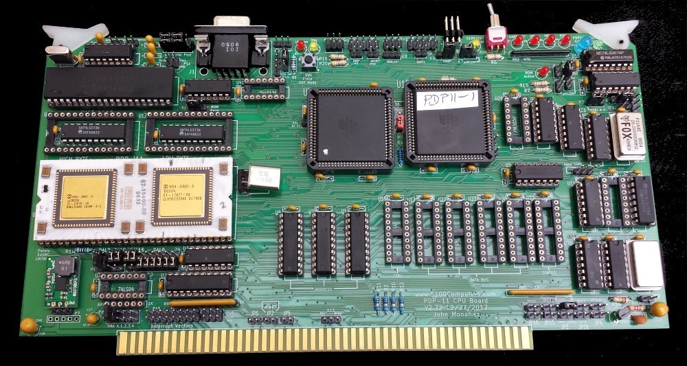
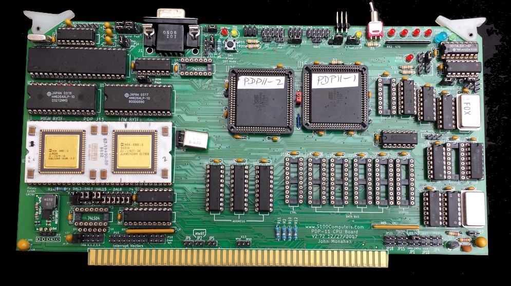
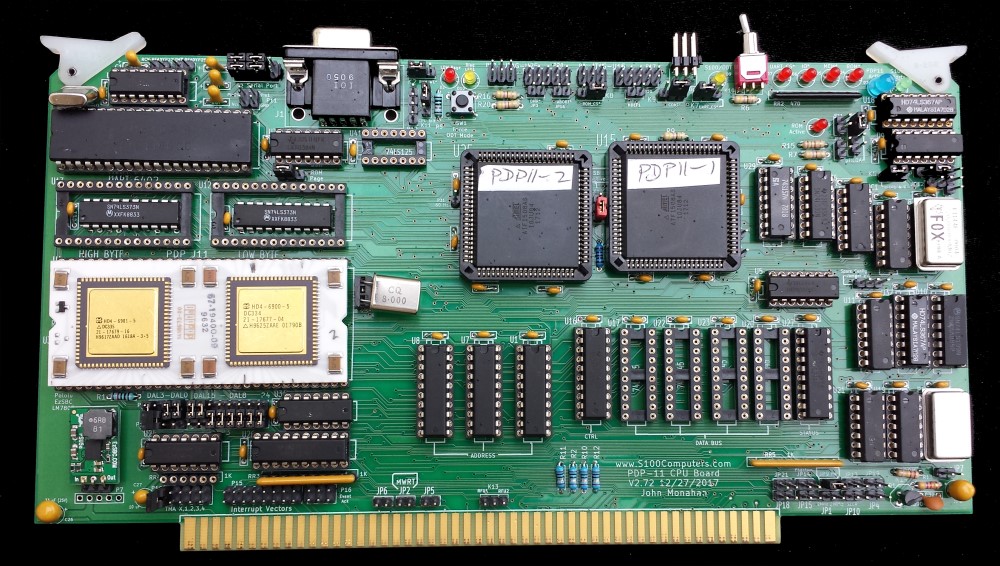
The PDP- J11 S100 Bus CPU V2 Board.
  
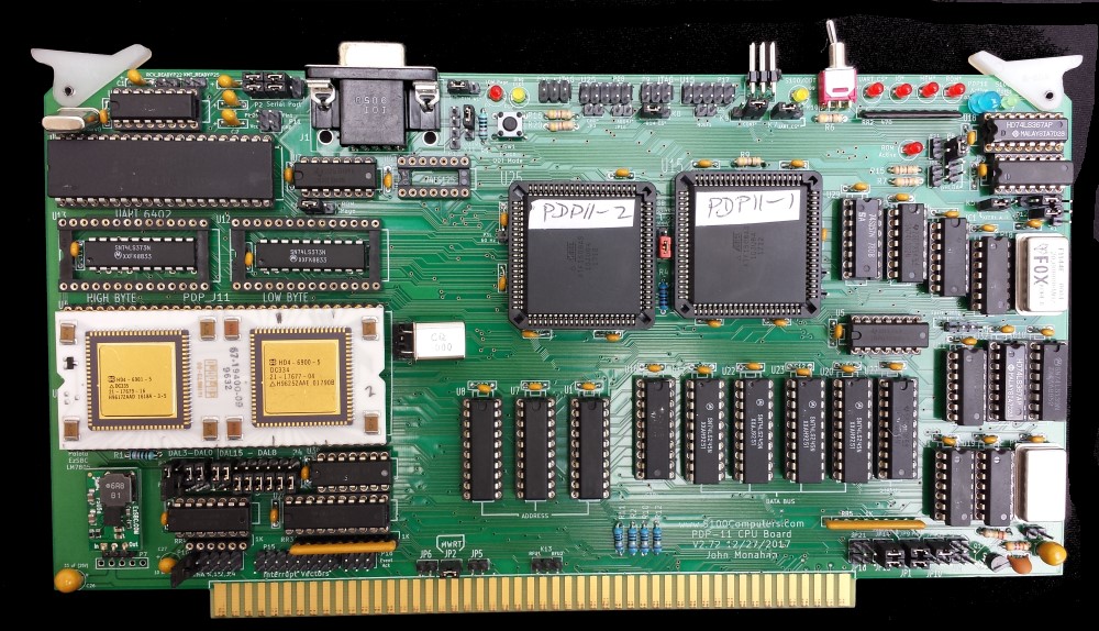
  Final Board
    
This is the second version of our original PDP-11 CPU Board.  It is essential that you become familiar with everything on that page before building and using this improved version of that board. The major modifications added to this "V2" board are:-

1.    The three 22V10 GALs on the V1 were condensed into a second 1508 CPLD.  There are no GALs on this board
2.    Code within this second CPLD allows for the handling of external bus interrupts similar to how Digital did it for their PDP minicomputers. 
3.    An Event Timer circuit and interrupt is now placed on this board and behaves exactly as the circuit on a Digital DL-11W Serial board
4.    A 6 pin ribbon cable connector is provided to directly interface with the PDP11 Support Board for serial port interrupts.  
5.    The board resets the CPU correctly with a bus hardware reset.
6.    The board can output to a port to completely remove the onboard monitor ROM – and thus not interfere with Digital OS software.
7.    The board can output to another port to set the upper/lower half of the 28C64 and so effectively get almost 2x more code in the EEPROM.
8
.    There is also a push button switch to force the CPU into ODT mode.

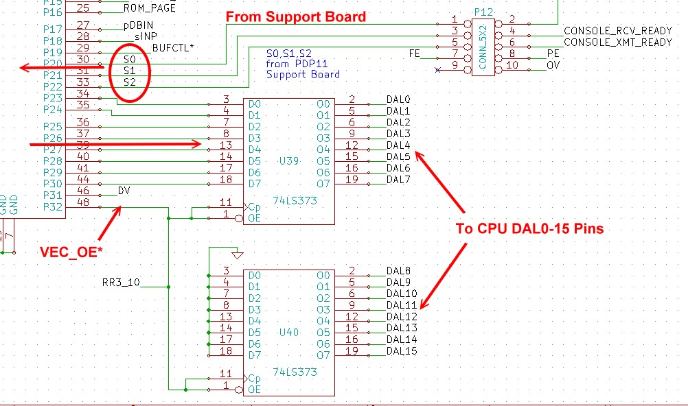
Apart from the addition of a second CPLD the main addition to this board over the V1 board is that this board now has is the ability to deposit an interrupt vector address directly on the PDP11 CPU DAL0-DAL15 pins. The two 72LS374 buffers  that do this (U39 & U40) reside under the two ROM's.  Space is tight on this board so they must be soldered directly to the board within the ROM sockets themselves. Here is a picture of the relevant circuit.
    
 nt Vectors Circuit
  
How interrupts are handled on PDP11 minicomputers is a complex process, rather than repeat things on this page, please go to here on our PDP11 Support Board page for a full explanation.

To recap from that page -- the CPU on this board will issue the unique INTA vector request shown below.  This will activate the two buffers and place the de-multiplexed S0,S1 & S2 interrupt vector RAM address on the  CPU DAL0-15 lines. During this brief time all data in from the S100 bus is blocked.

FIELD INT_VEC = [VEC_DAL7,VEC_DAL6,VEC_DAL5,VEC_DAL4,VEC_DAL3,VEC_DAL2,VEC_DAL1,VEC_DAL0];
FIELD INT_CODE = [S2,S1,S0];

!VEC_OE = LAIO3 & LAIO2 & !LAIO1 & LAIO0 & !BUFCTL;           /* Instruction INTA vector (1101) read request */


TABLE INT_CODE => INT_VEC {
         'b'000 => 'h'38; 'b'001 => 'h'38; 'b'010 => 'h'38;   /* S2,S1,S0 => Active LOW */
         'b'011 => 'h'38; 'b'100 => 'h'38; 'b'101 => 'h'38;
         'b'110 => 'h'30; 'b'111 => 'h'38;
          }

It is absolutely critical that this process is fast and 100% reliable.  Directly interfacing the above buffers to the CPU lines really helps this process.  The S100 bus is actually not involved.

Step By Step Building the PDP-J11 V2 CPU  Board
The build instructions are fairly simple for this board. It is essentially the same as for the original PDP11 board. However because it is a complex board building it should not be rushed.  As always, first examine the bare board carefully for scratches or damaged traces, use a magnifying glass if need be.  A broken trace is almost impossible to detect by eye on a completed board.

Build the board up in functional steps. Avoid the temptation of adding everything at once and popping it into your S-100 box. We will set the board up as a true S100 bus slave.  By programming the CPLDs and with the additional circuitry on the board it can in fact run it as a bus master.  I will leave this arrangement to our more experienced users.

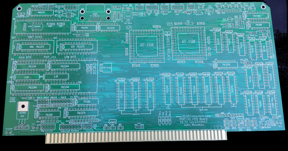
Here is a picture of the bare board:- 
        
  bare Board V2 
    
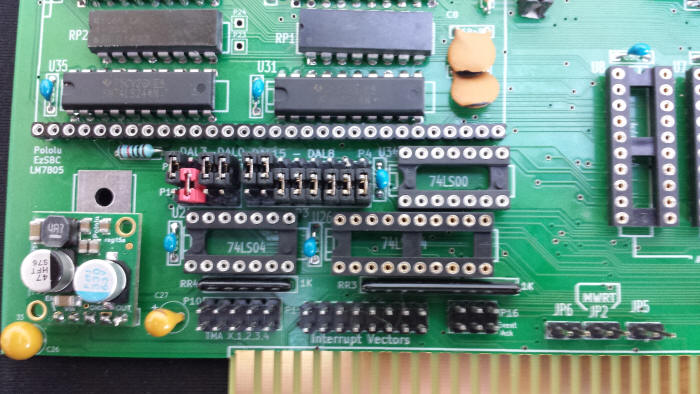
Solder in all the required IC sockets, resistors, the transistor Q1, resistor arrays, capacitors, jumpers, and the 5V voltage regulator.  For the latter you can use (but I don't recommend) a 7805+heatsink approach (e.g.. Jameco # 924633, a L7805CV). Better to use a more modern switcher regulators such as the Pololu # 2850 (5V, 2.5A) or EzSBC.com # PSU5a (5V 2.5A).  Do not add the LED's yet. Be sure you put the resistor arrays in with the correct orientation of pin 1 and check their values before soldering (they are difficult to remove).  Insert all jumper arrays. Be sure and have pin 1 of the CPLD socket on the LHS. For prototype boards I typically use common Aluminum Electrolytic caps. For the final board I use the corresponding Tantalum caps.  Be sure you have the + side of each cap correct -- particular C1, C6, C5 & C2.  Note K10 can be used with a 3 pin jumper, but it's best to use a small switch (see the picture below).  Be sure you have the push button micro switch SW1 in its correct orientation. See the schematic. If the board is to be used in slave mode only, you should in theory, not use the pull-up 1K resistors for the TMA lines (RR4).   However I find the 1K resistor load on each line with the 1K on the Z80 board is OK for its OC drivers to work fine. If you like, use a linear pin socket (see below). With the board configured as a bus master these lines must be pulled up, so add RR4.

Do NOT add sockets for U35,U31,U30,U37,U40,U39 & U28, RR1 & RR2.  We will (later) solder these components directly to the board (under the CPU and ROMs).
  
For prototype boards I generally use "double swipe" IC sockets. For a critical board like this I prefer to use "Machine Tooled" IC sockets.  However they are more expensive and you have to be particularly careful not to bend the IC pins.  The two clock oscillators can have their own special sockets (e.g. Jameco #133006) but actually I find the "Machine Tooled" IC sockets make a better connection.  I in fact solder the 2MHz oscillator (P1) directly to the board since it will never be changed.  For the sockets that have IC's under them you need cut out the cross bridge of the 40 pin or 28 pin sockets (see below) and trim the inside up with a file.  The spacing is very tight so check before you solder the socket in place.  (The alternative was a 4 layer board).
 
Place the board in the bus. Check the voltage to sockets on the board is about 5V by placing the board in your S-100 system using an extender board. With no load you will typically get 5.00V  (+/- 0.2V).  BTW, your system should boot and run correctly with its Z80 master CPU board. If not, you have a serious solder bridge somewhere on the board.  Before you do anything else with a magnifying glass go over every socket on the board and examine for proper solder joints. I like to "reheat" each joint just to be on the safe side. The silk screen/varnish on these boards us quite thick. It's easy not to have a good solder joint for the ground pins.  Double check.   Extra time here will save you hours later. 

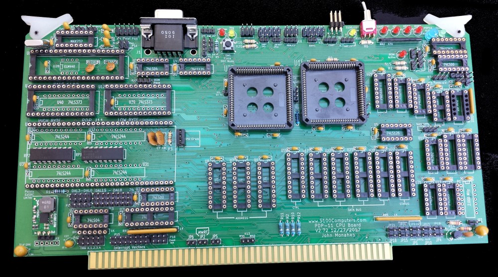
Next insert all 10 LED's. Before soldering them in place ground one at a time pins 3,5,7,9 & 11 of U18, pin 13 of U32, on the CPLD side of resistor R7 & R20 and pin 2 of K10,  to be sure they are all OK.   (I always use a blue LED for D3 "Board Active"  in my systems).   Solder in both 2.2K Resistor networks (RP1 & RP2).  Check each pair of pins across the chip is 2.2K Ohms.  Be sure its not a bus resistor network.  Here is a picture of the board at this stage:-
  
  Build Step 1 
    
We will first construct the basic circuit required for the master/slave S100 bus flip.
Please remember that for 3 or more pin jumpers, pin 1 is always the square pad.  It is not necessarily the one on the top, or LHS.  

First insert the CPLD in socket U15 taking care that pin 1 is in the center LHS.  Program this CPLD with the code provided at the bottom of this page.  If you are using a virgin CPLD you probably don't need to program it first but to be on the safe side you don't want input/output gate conflicts with a previously programed chip.  With no chips/jumpers on the board this is never an issue.  Be sure you use the correct connector/code to program it.

Next insert the second CPLD U25.  and program that one the same way.

The Z80 must boot up correctly with the two programmed CPLDs inserted.

You can directly solder in the 2MHz Oscillator at this stage.   Leave it above the surface of the board in case there is a card guide issue.

We now need to add the input address line buffers (U30, U37 and U36)  as inputs to this U25 CPLD.  These chips must be soldered directly to the board (under the CPU and UART chips).  It is critical you are sure these buffers are OK. If possible pull chips from another working board, just to be sure. 

We may as well also install the Interrupt Vector buffers U39 and U40 (74LS373's), and the "power on buffers" U31 & U35 (74LS244's).  All these chips should be known working chips before being soldered directly to the board. 

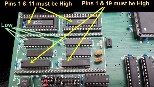
Install the "Power On Jumpers", P4 pins, 1-2 and 3-4. P3 pins, 5-6, 7-8, 8-10, 11-12, 13-14.   P20 pins, 1-2,  5-6,7-8.     P20 pin 3 to P4 pin 2. (See below and here for an explanation of these jumpers). It is absolutely essential that pins U39, U40, U31 & U35 are normally inactive.  Check the pins as shown here.
       
  Build Step 2
  Img8
     

Add U3, U19, IC1, U21, U5, U33, U34, U36 and U18.  Jumper P10 1-2 and K5 1-2.   Add K14, 2-3 (assuming no Support Board currently).
In your Z80 monitor use the "O" command (or however in your system you pass control over to an S100 bus  slave device), check that that jumper pin P10 1-2 goes from LOW to HIGH.  Hit reset,  it should flip back to LOW. 
   
Add the 20MHz Oscillator P18.
Jumper JP9. Add jumper K11 1-2 and K7 1-2.  Jumper P8 1-2 (top two pins) and K6 2-3 (right two pins).
Now with the "O" command the LED D1 "ROM Active" should light up as well as LED D3 "PDP Active". (The others are undefined).
The Z80 master monitor should "hang" after displaying "
TMA line 0 active".
A reset should turn off all LEDs.   Here is a picture of the board at this stage:-
   
  Build Step 3
        
Next we will add the UART serial interface to the board.
Add U2 (the MAX232N chip).  Add U6 (the UART). Add U26, U10, U11, U9.  The add U1, U8 and U7.
Jumper K12 1-2. 

Set the switch K10 (or jumper) 2-3. With power, the LED D9 should NOT light up.
When you press the button SW1 pin 9 of the CPU socket should go from low to high.

Assuming you will initially be using the DB9 serial socket J1, jumper P2 1-3, 2-4, 5-7 & 6-8. See the picture below.  BTW, the P2 connector is pin for pin compatible with the serial connector on our Serial I/O board so later you can hookup a ribbon cable internally in your system to a serial DB9 connector at  the back of your box.
     
Jumper K9 2-3. Power up the board and check you are getting a ~156.24 KHz clock,  (156/16 KHz = 9765  or ~9800 baud) if you have a frequency counter on pin 40 of the UART (U6).  At least check you are getting a continuous pulses with a logic probe on pin 40. 
 
To start, add a 3-8 MHz crystal to pins X2.   Then carefully add the J11 CPU chip.  The pins on this chip are delicate so be very careful inserting the chip into the two rows of sockets.  Double check you don't have any chips in backwards. Most of these CPU work well in the 10-12 MHz range but we will start off low. If difficulties below,  drop the frequency.

Next connect a serial connection to a TTY terminal on your PC to the top DB9 connector J1. 
There are many programs. I like "Absolute Telnet" but the free PuTTY or Tera Term ones are also excellent. 
The serial connection to this board must be (in the default mode USED here), 
9600 Baud, 8 data bits, 2 stop bits, and no parity.
If you use a USB to Serial connector/cable in most cases you need only specify the Baud rate and stop bits.

Power up your system and with the Z80 "O" command transfer control to this board.
You may see random characters on your TTY terminal.  Briefly press the SW1 button, you should see the J11 ODT Console signon prompt '@'. 
You may actually see the '@' signon with the 'O' command.
In every case however the SW1 button will present the ODT '@' prompt.

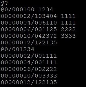
Since the is no RAM on the board at this time all you can do is display the CPU registers.
Type R0 followed by a '/' . You should see the current (random) value in the CPU's R0 register.
Typing further LF's (Crtrl j's), will cycle through all the CPU registers. 
Here is an example output:-
   
 Build Step 3e
  
You can change the (octal) values by entering a new value followed by a Ctl-J (LF) and go back and confirm the change(s).
If you press your system reset button you should be able to repeat the above process.
 
Here is a picture of the board at this stage:
   
  Build Step 4
           
It is absolutely essential you get the above diagnostic test working before going further. The ability to interact as described above is a fantastic advantage of this CPU chip.  Most of our other CPU boards require almost a complete build of the board before getting any life out of them.  Debugging such a non-functional board can be problematic.   There are few chips on the board at this stage. It should not be too hard to identify a problem.  Upon obtaining control of the bus. Pin 1 of U7 must go low. Pin 11 of U7 must be pulsing. Jumper K11 pin 2 must go from Low to High (INIT*, pin 33 of the CPU) after a hardware reset.  Pin 9 of the CPU (HALT*) should be Low (unless SW1 is pressed).

If you do not see the signon prompt, your first suspicion should be the serial connection to your PC.   Disconnect the serial connection and try a loop test or a connection to another serial port (ideally at 9600 baud). Be sure you have all the jumpers exactly as described and shown above. Check that pin 25 of the UART pulses low when you enter a CR from your PC.   BTW, if you have the SMB you can jumper this boards P10, 3-4,  and use TMA0* on that board for the PDP11 to get control of the bus.

Do not go forward until you get the above ODT signon test to work.

We will next (temporarily) add 16K of local RAM to the board to further test/flush out our circuit.  You could in fact skip this step since in the end we will be using only RAM on the S100 bus.  However I really recommend you go the extra mile.

Add two HM6264LP-10 (16KX8) static RAM chips (or their equivalent) to U12 & U13.
Jumper P11 1-2 (the jumper should be vertical on the LHS connecting Vcc to pin 26 of the RAM chips).
Jumper K2 2-3 and K8 2-3.
Boot up the CPU with the usual "O" command.
You should be able to see and modify RAM starting at 0H in RAM.
Here is a picture of the board at this stage:-
     
  Build Step 5
       
Below we change the 16 bit words at 0-10H in RAM and then verify that we have done so.
Remember all values are in octal. All addresses must be on an even byte boundary.
      
 Build Step 4a
    
If you get this far you are well on your way to having a functional system.  The next step is to replace the onboard 16K of RAM with access to the S100 bus RAM. 
For this we need to add the S100 bus data buffers and for the first time call upon the CPLD to step in and handle RAM I/O requests.

First remove the onboard RAM chips U12 & U13. We will not need them any more. Remove Jumper P11.
For the (later) onboard ROMs jumper K2 1-2. Leave K8 2-3 for now.
Add U29 and U32.  Add U24 (To prevent false interrupts).  Repeat the above ODT signon to display the CPU registers

Add U16 and U27 (the S100 bus status and control lines). 
Repeat the above ODT signon test from power up to display the CPU registers.

Here is a picture of the board at this stage:-
        
  Build Step 6
   
Add U17, U20, U22 and U23 (the data buffers to the S100 bus).  
At this point all chips should be on the board except the two ROM sockets U13 & U12 and U41.
 
Add the MWRT jumper JP2. (Note this assumes your Z80/bus master hands over the MWRT signal to the current slave).
Add JP1, JP14, JP15, JP13 and JP12 -- to be on the safe side.

Repeat the above RAM read/write test.
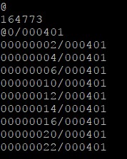
Go back to your Z80 and fill RAM 0-100H with say
01H. Then check with the PDP-J11 that you see these values (000401 octal). 
Here is a picture of what you should see for RAM at 0H.
  
 11 In RAM
   
Within the ODT change a few values to (say)
123 octal.
Go back to your Z80 and confirm the value has changed. You should see
53 00, 53 00, 53,00....
Remember within the ODT monitor all reads/writes are words on an even address boundary.
Here is a picture of the board at this stage:-
        
  Build Step 7
         
BTW, we noted for the original PDP-11 CPU board, that the J11 designates addresses 3F
E000h - 3FFFFFH as port IO's. We need to "translate them" to 8/16 bit ports 0000H-1FFFH on the S100 bus.  This is done in hardware and is completely transparent to the J-11 CPU.  The following circuit does the trick:-
        
  Port Address Lines 
  
Unlike the original PDP11 CPU board the address line A12 is not altered so we get the full PDP11 port address range
0-1FFFH.

We will now start to utilize more of the code in the U25 CPLD.
We need to be especially careful with the onboard UART (U6) address lines.  For our original (V1) PDP11 CPU Board any an all address in the range 3F
FF70H to 3FFF76H went directly to the J11 for console/UART IO (and not act as ports on the S100 bus).  For this board there are two different situations:

If this boards UART is "acting alone" (and only in status bit mode), than, as for the V1 board, all addresses in the range
3F1F70H to 3F1F76H  are blocked S100 bus access and go to/from the onboard UART.  If this board is working with our PDP11 Support Board  and we wish to utilize the default ODT UART on that board, then all the UART data ports on this board (3F1F70H to 3F1F76H) are blocked.  Which option is determined by the jumper K14 (in the middle of the board.  It is essential that this jumper is always in the correct position.  If it is not, the V2 PDP11 CPU board will not be able to obtain ODT console data and will hang.  So remember:-
    
  Support Board Jumper
    
I know this is going to be a source of error as people forget this requirement. The only way around this would be to have some signal value sensing from the Support Board coming across via the P12 connector -- perhaps in a later version of this CPLD code.  Here is the relevant code in the U25 CPLD:
 
                                                                        
!!UART_ADDRESS = ((LA21_19 & LA18_16                                      /* Always 3F */
                 & LA15 & LA14 & LA13 & LA12 & LA11 & LA10 & LA9 & LA8    /* Note address lines before U29 (FFxx) */
                 & !LA7 & !LA6 & !LA5 & LA4 & !LA3 &
SB_ACTIVE)           /* All 4 U6 ODT UART Ports, 10 to 17 do NOT go to the S100 bus */
                                                                          /* The ODT UART is on the Support Board. This is an extra UART */

               #  (LA21_19 & LA18_16                                      /* Always 3F */
                &  LA15 & LA14 & LA13 & LA12 & LA11 & LA10 & LA9 & LA8    /* Note address lines before U29 (FFxx) */
                & !LA7 & LA6 & LA5 & LA4 & !LA3 &
!SB_ACTIVE));           /* All 4 U6 ODT UART Ports, 1F70 to 17F7 do NOT go to the S100 bus */
                                                                        
 /* The ODT UART is U6 on this board */

!UART_CS      = !UART_ADDRESS & !LBS_IO & !XFERII;                        /* UART is in range (No S100 bus ports allowed) */


Whenever
UART_CS* is low the S100 bus buffers (U17, U20, U22 & U23) are inactive and data comes across from the UART directly on the onboard CPU.

Set  K7 2-3 and set K14 2-3 (assuming no support board at the moment).  Repeat the above RAM RD/WR test.

As described for the V1 PDP-11 CPU board, upon power up the CPU memory management facilities are not active.  Available RAM is in effect from 0H to DFFFH.   We will place the onboard ROMs at
C000-DFFFH.  So any and all addresses in the range
C000H to DFFFH will go to the boards onboard ROM's and not input RAM data from the S100 bus.  Again we use the U25 CPLD to flag this situation as  ROM_ADDRESS*.  To be sure its working, use the ODT monitor command to examine RAM at 140000 (E000H).  Jumper K8 1-2. As you examine RAM in that range pin 2 of jumper K8 must pulse.   If not check the code in the U25 CPLD.   Jumper K9 1-2.

Burning the Onboard EEPROMS
Program two AT28C64 EEPROMs with the latest PDP11 monitor code available at the bottom of this page.  Please read here about this monitor before proceeding. Be sure you correctly burn the High/Low bytes with your PROM programmer. Insert the 8KX8 EEPROMS (AT28C64). Make sure the High byte is in U13 and the Low byte is in U12. Jumper K8 from now on, should always be set 1-2.

Please note, versions V2 and later of the PDP_MON.MAC code allows you to use a High and Low 4K page of the 28C64 EEPROM.  This in effect doubles the capacity of code that can fit between
C000H and DFFFH in the CPU's RAM space.  Programming these EEPROMs requires 4 files and is quite tricky.  See here.    Unless you are very comfortable with that process, during this build process start with the V1.5 version of the monitor which does not utilize this High/Low page feature.

Alternatively
just use the low page of the EEPROM to start with.  To do so, assemble and make a .bin file using:-
 
"
PDP_MON_LOW_PAGE.MAC"  found at the bottom of this page.  Do a "normal" Even/Odd EEPROM burn. 

Note the High/Low ROM page feature requires K12 jumpered 2-3.  For the V1 or just low page option, use K12 1-2.  Be sure the K10 Jumper/Switch is such that the LED D9 is on (for active Low Page). 
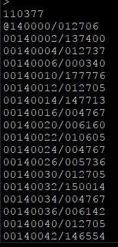
Reading RAM at 140000 (D000H) should show something like this, (if you use the V1.5 version of the monitor) :-   
 
 EEPROM Data

This corresponds to the following code at the start of the PDP11 Monitor (V1.5).

140000 012706 137400          Start: MOV   #CPU_STACK,SP    ; Setup stack at BF00H (for now, below ROM ORG at C000H)
140004 012737 000340 177776          MOV   #&00E0,@#PSW     ; Block ALL Interrupts (Clear bits 7-5)
140012 012705 147713                 MOV   #Signon,R5       ; Point to Signon Message
140016 004767 006160                 JSR   PC,PrStr         ; Print string
140022 010605                        MOV   SP,R5            ; Show current SP
140024 004767 005736                 JSR   PC,PutWord_R5
140030 012705 150012                 MOV   #Signon1,R5      ; Point to Signon Message finish
140034 004767 006142                 JSR   PC,PrStr         ; Print string
140040 012705 146554          Loop1: MOV   #MainMenu,R5     ; Point to Main Menu
140044 004767 006132                 JSR   PC,PrStr         ; Print string


If the bytes are not the same as you have in your monitor code then the is probably an addressing problem with your EEPROMs. 
Note the start code for versions V2 or later is different -- see your PDP_MON_LOW_PAGE.LST file printout.

If you are satisfied that you are reading your ROMs correctly use
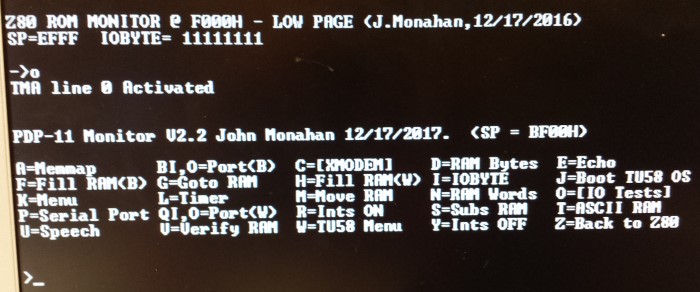
140000G to transfer CPU control to your onboard ROM Monitor.  You should see something like this on your TTY terminal.
     
  V2 main menu 
      
I have done many prototypes of this board as it evolved in complexity.  Seeing the above display is always a moment of relief. Enjoy it!

At this point all IC's should be on the board except U41 and the ELM timer chip under the UART (see below).
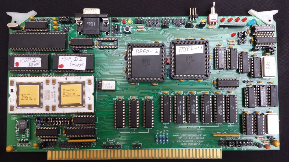
Here is a picture of the board at this stage:
    
  Build Step 8 
    

A PDP11 Power On Recap.

As we noted for the original PDP11 CPU board, any and all addresses in the range (3F)E000H to (3F)FFFFH are understood to access I/O ports by the J11.  This board converts addresses in that range to the corresponding S100 bus I/O ports in the range 0 to 1FFFH. Only addresses 0H to (3F)DFFFH are available to RAM.  Further within the (3F)E000-(3F)FFFH block, (3F)FFE0H to (3F)FFE8H are "System Registers" (see below).  Further complicating matters when the J11 first powers up only the address range 0H to FFFFH is available (16 bits). The CPU internal memory management registers must be programed to access the 4MB (in 64K blocks).  So in startup mode accessible RAM is 0H to DFFFH. It is important to remember that any and all addresses in the range E000H to FFFFH are automatically translated to address (3F)E000h to (3)FFFFFH. In other words, with memory management inactive, if the address lines A15 & A14 are high then address lines A21-A14 are all high - no exceptions.  The J11 CPU lowers LBA_IO* for I/O access (Pin 1 of U29).

So far we have been running the CPU at low speed with a 3-8MHz (see above).  We will now active the CPU's wait state capability by jumpering K9 1-2. While not normally used with our current high speed RAM boards, that jumper does allow us to utilize S100 bus wait states.  This can be seen if you use the monitor "D" command to display RAM and hit the SMB "Stop Button".

Next we need to have the CPU jump to the EEPROM and run the code from there in non-ODT mode. 
I will repeat the write-up on the J11 "Power Up" circuit we described for the V1 PDP11 board for clarity.

Normally upon power the CPU looks at the very initial values of its DAL0-DAL15 lines for startup information. On pages 8-7 to 8-8 of the PDP User Guide there is a description of a circuit that allows you to define where the CPU starts in its 64K RAM space.  Upon power up the CPU inputs the DAL 0-15 lines when a General Purpose Read  is placed on the AIO03-AIO0 lines (1110) and the Read code on DAL 0-7 is 000 or 002.  This is a single read/pulse.  The PDP interprets the 16 bit data as follows:-
  
 Power Up Bits

We incorporated the following circuit on the board to trap these situations:-
Here is the circuit:-
     
 Power Up Circuit
   
The U25 CPLD relevant code is:-

!reg0.d = !DAL0 & !DAL1 & !DAL2 & !DAL3 & !DAL4 & !DAL5 & !DAL6 & !DAL7
        # !DAL0 & DAL1 & !DAL2 & !DAL3 & !DAL4 & !DAL5 & !DAL6 & !DAL7;

reg0.ar = !MASTER_RESET;
reg0.ck = ALE;

!POWER_UP = !reg0 & LAIO3 & LAIO2 & LAIO1 & !LAIO0 & !BUFCTL;
 

We use the above CPLD code to provide the one time only, initial pulse to the two 74LS244's. The input values are determined by the jumpers P3, P4 and P19, P20. Way back at the start we jumpered P20 & P19 to always power up in ODT mode. In particular  P20 pin 3 to P19 pin 2.  We will now set P20 Pin 2-3.   If both the DAL1 & DAL 2 lines are high the CPU on power up will bypass the ODT console mode and directly jump to the address boundary defined by DAL15-9. This should always happen UNLESS the J11 HALT (pin 9) is high (SW1 pressed).   Depending on the jumper/switch K10 the PDP monitor will either input/output through  the UART (LED D9 off) or to the S100 Bus Console-IO board (LED D9 on).  
 
    V2 Main Menu 
 
Please read about the PDP11 Monitor commands here.  Remember if you utilize the High/Low Page ROM options jumper K12 2-3.

You now have the PDP V2 board running essentially as the original "V1" board.

Remember if you are in "S100 Bus" mode and you press the pushbutton SW1 you will always force the PDP11 into ODT mode where output will only appear via the onboard UART to your TTY terminal.  If the serial connection is not in place the board will appear hung.

Also remember there are
S100_ONLY and ODT_ONLY equates in the PDP11 ROM Monitor. Be sure it is set to false if you want the above SW1 switch option to work.

The PDP11 Event Interrupt Circuit.
The next step is to implement PDP11 style interrupt timer.  This is where this board differs considerably from the original V1 PDP11 board. Before you do this you need to carefully understand how the event timer interrupt works in PDP11 systems.

First let us look at the Timer circuit.  This is a circuit that emulates the timer on a DL11-W board in a Digital Unibus system.   Back in those days there were no RTC chips, timers supplied regular interrupt pulses to the CPU which kept track of time.  That is why when you signed on to an Operating system of that era you had to enter the (starting) time and date.  However this interrupt function was deemed so important by Digital that they gave the J11 CPU its own input pin (EVENT*, pin 8) and interrupt.  It's important to appreciate that in spite of its name,  this interrupt has nothing to do with the other interrupts/circuits we will discuss on the PDP11 Support Board.   Furthermore its up to the software to decide what to do with the interrupt.  In their Documentation Digital calls the interrupt the "Line Clock" interrupt. It is assumed to run at 60 Hertz (in the US). In all Digital software the Line Clock interrupt will cause the PDP-J11 to vector to RAM location 40H, (100 Octal).  We will discuss this in a moment, but the response from there can be a simple Interrupt return (IRET)/Ignore or an update of the time and date. 

First let us look at a timer circuit I used.
  
  ELM Timer Circuit    
  
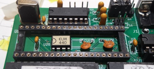
I experimented with a number of circuits.  In most cases I found the 60Hz pulse was not accurate and lead to second/minutes drift over time.  In the end I decided upon the simple single one chip approach of the ELM440.  It's only an 8 pin dip and fits conveniently under the UART socket on the board as shown above. This specialized chip is not available from most common vendors but can be ordered directly from ELM here (in Canada). Its not cheap ($8 each), but it seems very reliable/accurate.  Here is the ELM440 datasheet. The 60Hz signal from U28 will go directly to the U25 CPLD where it is processed as described below.

Solder the chip directly to the board. Also add U41.  Here is a picture of the arrangement.
       
  Elm Chip
   
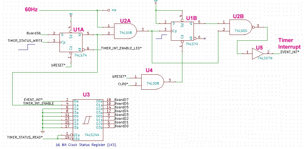
It is simplest to understand if we first look at a hardware approach I used in an early PDP11 timer circuit shown here.
     
  Timer Interrupt Circuit
                   
In the PDP11 Digital Unibus system,  the timer interrupt must first be activated in software by setting
bit 6 of port 66H High, (the Timer Status Register) .  This we do by setting the U1A Flip Flop (FF). Then (and only then), can the U1B FF be clocked by a timer interrupt every 60 Hertz.  This will cause a pulse on U5 pin2 which travels over an S100 bus interrupt line to the V2 CPU board and eventually to pin 8 of the J11 CPU.  The CPU upon receiving this interrupt, when interrupts are activated, always branches to location
40H. Interrupt vectors on the J11 consists of two 16 bit numbers, first the interrupt routine RAM location and second the PSW word. Again always -- no exceptions. You need to carefully study the Digital PDP11 User Guide to understand this process.  As an example I wrote a simple timer routine in our PDP11 Monitor that simply beeps the "bell" every 5 seconds on systems with our Console IO board.  If you say, display with the RAM with the monitor "D" command it will beep every 5 seconds during the display.  (BTW, with the older V2 Console IO board there is a slight delay during the beep. There is none with the new V3 version of that board, see here for more details).  Note, the 60Hz signal is available on the board at P31.

Anyway here is the relevant PDP11 Monitor event code.

align
EventRoutine:
        MOV R0,-(SP)
        ADC @#&44            ; Remember we had the vector setup to set the carry bit so this increments
        ADC @#&46            ; location 44H (104 octal) and carry over the overflow to carry and then adds it to 46H
                             ; so this is a sneak increment of a 32-bit integer (you can’t use the INC
                             ; instruction as it does not update the carry bit). Can count to over 8 days!
                             ; (Trick from Peter Schranz, Switzerland)
        CMPB #&01,@#&45      ; We get to 00000010,00000000 for RAM at 45+44 in ~ 5 seconds
        BHI Event1
        CLR @#&44            ; Reset Timer
        MOV #&07,R0          ; Send Bell/beep to CRT about every 5 seconds
        JSR PC,CONSOLE_OUT
Event1: MOV (SP)+,R0
        RTI


Because the routine is run so often it has to be very fast.  It uses a unique trick to increase a stored 32 bit value in RAM location
44H-47H.  (This kind of thing you will find a lot of in Digital PDP11 assembly code.  RAM was scarce back then).

We have one remaining thing to do.  We need to let the above circuit know the event was processed and clear the U1B FF.  The PDP11 issues a special code when it recognizes a timer event interrupt. Then -- and only then,  will this pin combination exist.

!EVENT_ACK = !LAIO3 & LAIO2 & !LAIO1 & LAIO0 & !DAL7 & DAL6 & !DAL5 & !DAL4 & !DAL3 & !DAL2 & !DAL1 & !DAL0;

This combination is recognized in the U25 CPLD and will send a low CLR0* low signal to U4 clearing the U1B FF.  The whole process repeats again (at a rate of 60 Hertz). 
I want to stress that all of the above is a unique process and has nothing to do with "normal CPU interrupts" we will next when we go to the PDP11 Support Board Interrupts.

That was how I initially setup the hardware on an early prototype board to understand and debug the process. 
On this final board I have brought the U1A and U1B FF's directly into the CPLD.  Here is the equivalent CPLD code in U25.

Pinnode = reg7,reg8;
Pinnode = TIMER_ENABLE;
Pinnode = TIMER_STATUS_BUFFER;                                /* Note TIMER_STATUS_BUFFER is local to this CPLD. */


!TIMER_ACK = !LAIO3 & LAIO2 & !LAIO1 & LAIO0 & !DAL7 & DAL6 & !DAL5 & !DAL4 & !DAL3 & !DAL2 & !DAL1 & !DAL0;

!TIMER_STATUS_BUFFER = LA19_21 & LA16_18                                      /* Always 3F */
                     & LA15 & LA14 & LA13 & LA12 & LA11 & LA10 & LA9 & LA8   
                     & !LA7 & LA6 & LA5 & !LA4 & !LA3 & LA2 & LA1 & !LA0;     /* Ports 1F66 */


TIMER_STATUS_WRITE = !TIMER_STATUS_BUFFER & sOUT;            /* Byte Write FF66H = 1F66H */
!TIMER_STATUS_READ = !TIMER_STATUS_BUFFER & sINP & pDBIN;    /* Byte/Word Read FF66H = 1F66H & 1F67H */

!STATUS_READ_BIT7 = !TIMER_EVENT;                            /* Bit 7 of Low Byte for Timer Status Port (0=Interrupt) */
!STATUS_READ_BIT6 = TIMER_ENABLE;                            /* Bit 6 of Low Timer Status Port (0=Timer Active) */

reg7.d       = DO_BIT6;
reg7.ck      = TIMER_STATUS_WRITE;
reg7.ar      = !MASTER_RESET;
TIMER_ENABLE = reg7;

reg8.d       = 'b'1;
reg8.ck      = TIMER_ENABLE & HZ60;
reg8.ar      = !MASTER_RESET # !TIMER_ACK;                    /* Clear Interrupt when EVENT_ACK is returned */
!TIMER_EVENT = reg8 & TIMER_ENABLE & HZ60;                    /* Sent interrupt to CPU */


The above CPLD code does 5 things.  It recognizes the 60Hz input, sends the status of bits 6 & 7 directly to the DAL inputs of the CPU (when port
3FF67H is read), sends the interrupt to the CPU and when done clears the interrupt.

Brice Hassenstab has pointed out that the 8 pin PIC12F609 CPU can be programmed to produce a 60Hz 50% duty cycle square wave on pin 7 similar to the above ELM chip. It's not a direct replacement for the ELM chip (doesn't output the 1 Hz on pin 6) but will work fine on this board. You also don't need the crystal X1 also since this PIC uses its internal oscillator.  The HEX file to program the chip is provided below.

Setting  the High/Low Page ROM
Within the code for the U25 CPLD is a routine to switch to the High or Low ROM pages in the U12 & U13 28C64 8kX8 ROMs.
To select a High page one inputs from port
E0E4. To select a Low page one inputs from port E0E5
Upon reset the default mode is the low page.  When the low page is active LED D2 is on.  The relevant CPLD code is as follows:

Pinnode = PULSE_PAGE_L;                                                       /* >>>> SET ROM ADDRESS LINE DAL13 HIGH -- E0E4H <<<<<<<<<< */
Pinnode = PULSE_PAGE_H;                                                       /* >>>> SET ROM ADDRESS LINE DAL 3 LOW -- E0E5H <<<<<<<<<< */
Pinnode = reg6;
                                                                              /* Code to page ROM in the PDP address space via Port E0E4H */

!PULSE_PAGE_H = (!LA0 & !LA1 & LA2 & !LA3 & !LA4 & LA5 & LA6 & LA7            /* E4 */
               & !LA8 & !LA9 & !LA10 & !LA11 & !LA12 & LA13 & LA14 & LA15     /* E0 (of E0E4H for HIGH Page) */
               & sINP & pDBIN);

reg6.d = 'b'0;
reg6.ck = !PULSE_PAGE_H;
reg6.ap = !MASTER_RESET # !PULSE_PAGE_L;
!ROM_PAGE = reg6;                                                             /* DAL13 HIGH for ROM. Activate upper half of 28C64*/

                                                                              /* Shadow back IN ROM in the PDP address space via Port E0E5H */
!PULSE_PAGE_L = (LA0 & !LA1 & LA2 & !LA3 & !LA4 & LA5 & LA6 & LA7             /* E5 */
              & !LA8 & !LA9 & !LA10 & !LA11 & !LA12 & LA13 & LA14 & LA15      /* E0(of E0E5H for LOW Page) */
              & sINP & pDBIN);


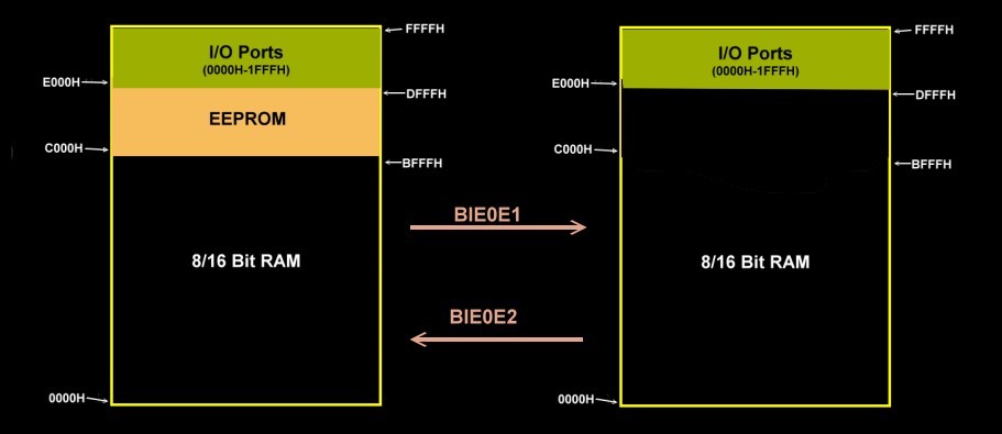
The same CPLD coding approach is used to shadow out (or back in)  the onboard ROM (ports
E0E1 and E0E2) .  This allows Digital software to occupy RAM from 0H up to DFFFH.


CPU Speed
You can at this stage now experiment with CPU speeds. The one thing I have noticed is that while the CPU is not real sensitive to clock speed, it is however, to the actual waveform going into its pins 36 & 37.  They must be 'clean'.  Sub-quality crystals, or, their connection really cause problems. In one of my two systems, the board seems to run rock solid with a S100 Bus Phi clock signal of 16MHz.  This is an active terminated IEE-696 S100 bus 10 slot motherboard.  However in my "main system", (a 21 slot active terminated almost fully populated motherboard),  I can only get to 12 MHz.  It really helps BTW if you replace the 74LS245's with 74S245's for U17, U20, U22 & U23.   I suggest you start at 8MHz and work your way up.
   
The PDP-11 Board Jumper Table
There are a fair number of jumpers on this CPU board and they need to be set carefully.  To run the board as a bus slave (with a Z80 master)  here is a typical jumper setup:-
            
 
Jumper   Function 
JP2Normally closed. Generate the S100 bus MWRT signal on this board when it is active.
JP1Normally closed. Generate the S100 bus 2MHz Clock signal on this board when it is active.
P11 Jumpers to accommodate RAM or ROM chips. For RAM J11 1-2. For EEPROM's leave open.
JP4,JP5, JP6,JP7Normally all open unless the board is a bus master.
JP13,JP15Normally closed to utilize the S100 bus Phantom Line. To be safe add JP15
K2 & K8RAM/ROM OE* & WR* signals. For RAM jumper both 2-3. For EEPROM jumper both 1-2.
K1 Normally 2-3
K9 Normally 2-3 during board for testing/assembly. Allow S100 bus wait states with 1-2
K7UART Select, Set 1-2 for core circuit testing. Normally 2-3
K5For slave mode 1-2
JP9Jumper after the U15 CPLD is programmed
K6,JP12Set 2-3 and jumper JP12
P8Set 1-2 and jumper JP13
P9 or P17 U15 CPLD JTAG programming socket. For Rockfield Research 1508 programmer use P9. Pin 1 is bottom left.
P27 or P28 U25 CPLD JTAG programming socket. For Rockfield Research 1508 programmer use P27. Pin 1 is bottom left.
P10S100 Bus TMA line to activate board. Normally 1-2 (also jumper 3-4) . Assuming TMA0 to activate board.
K4Currently unused. Set aside to configure Master/Slave configurations in CPLD code
P13Inputs from S100 bus Interrupt vectors. See PDP11 Support Board
K10/SwitchThis can be a mini-switch or jumper to determine where the PDP_MON monitor data I/O is sent
P2This a serial port connector for the UART with a pinout like our Serial board. If the DB9 socket is used it must be jumpered as described above.
K14VIP Jumper. Used to determine if PDP11 Support Board is present.  If so, jumper 1-2, if not 2-3.
K12Used to select Upper/Lower EEPROM. For debugging use 1-2. For page management use 2-3.
P22. P25These jumpers allow the onboard UART status signals to reach the P13 connector. Normally not jumpered.
K13, JP20, JP19Unused jumpers to S100 bus unused bus lines.
SW1 Pushbutton switch to force PDP11 into HALT/ODT mode.
K12 For the High/Low ROM page option 2-3.  Initially start with 1-2.
P31 60Hz timer signal from the ELM timer chip U28
P12 Currently unused. Can be used for configuration status bits

PDP-11 S100 Board Parts
The PDP-11 chip is not available from most vendors.  It is found on eBay -- either as the chip alone see here or it can be pulled from Digital boards.   It is almost always socketed on those boards. A typical eBay price is $100/chip. Most of the other components are common. I usually get them from obtained from Anchor Electronics and Jameco.  The 1508 CPLD's (#556-ATF1508AS-10JU84) from Mouser. The EML 440 clock chip can be ordered here (from Canada).  Shipping is via US mail, takes two weeks.

PDP-11 CPU Board  Bugs.
So far no bugs have been reported for this board. 

The ELM Clock chip is now very hard to find.  Brice Hassenstab has pointed out that you can program a regular
PIC12F609 chip  so it will output a 60hz 50% duty cycle square wave on pin 7 as needed for the interrupt timer U28 on the PDP11 cpu. He uses the 12F609 because of its internal oscillator. While it is not a direct replacement for the ELM chip (doesn't output the 1 hz on pin 6) it will work for this PDP11 board. You don't need the crystal X1 also since this PIC uses its internal oscillator. You can upload the .HEX file from the bottom of this page.
  
Notes.
1. Both CPLD's on this board allow you to add quite a bit of sophistication to the board.  That said , you have to be careful and completely understand what each CPLD pin actually does.  For example the U25 CPLD pin 49 (
ROM_ADDRESS*) allows you to completely remove the onboard ROMs from the board by simply inputting from port E0E1H.  This is done via the signal being passed on to the U15 CPLD (its pin 57) which internally goes to ROM_CS* (pin 58). Please see the code in both CPLDs.
Here is a picture of the memory map:-
   
  Memory Map

Please see here for more information.

2.  You need to be very careful displaying/altering "RAM" at
E000H to FFFFH.  Remember on the PDP11 it's not RAM, it's addresses I/O ports.  In particular the I/O ports E0E0H - E0E8H may blow the CPU out of the water due to master/slave switching, ROM switching etc. Even simple things like "displaying" RAM in the region will have unpredictable effects.  Remember on the PDP11 all "RAM" from E000H to FFFFH is actually first remapped to 3FE000H to 3FFFFFH and on the board converted to S100 Bus I/O ports 0000H to 1FFFH, always, no exceptions.

3. Peter Schranz/Switzerland alerted me to the fact that to run a Digital OS like RT11 you must activate an Abort interrupt if the CPU tries to access an invalid/inactive I/O port.  (It also does this for an invalid RAM access but we will assume we have at least 4M of RAM in our S100 bus system). This was a little unnerving as I had not anticipated this up to now.

Fortunately we have a jumper from the U15 CPLD to the Abort (pin 20) of the CPU.  It is not quite as clean as I would have liked,  but here is what I did.  On the U25 CPLD we have all the latched address lines coming in.  We make a "hit list" of valid port addresses.  We don't have a spare pin on this CPLD however.  However there is a pin we can do without -- SHADOW_ROM* (pin 24).  Its function is to remove the two ROMs from the CPUs address bus if required (for example before loading an OS like RT-11.).  I was able do double up this function with
ROM_ADDRESS* which also is passed onto U15 in the U25 CPLD.  So on the "new" schematic (see below) the U25 pin is labeled VALID_PORT and on U15 its pin is now labeled VALID_PORT.  No actual board modifications are required.

In the U25 CPLD we make a "hit list" of valid ports in our system.  If the PDP11 CPU addresses any of these ports
VALID_PORT is set high.  This signal travels to the CPLD U15 where its checked for being an I/O port address (!LBS_IO = LBS1 & !LBS0) and with !SCTL.  If low, the CPU is accessing an invalid port. The signal is passed on the Abort pin on the CPU (pin 20) via jumper JP16.  (It is also sent to the test point P14).  Here is the relevant WinCUPL code for both CPLDs:
  
U25 CPLD

FIELD IOADDR = [LA12..0];

!PROPELLER_PORTS     = IOADDR:['h'0000..0001];
!IOBYTE_PORT         = IOADDR:['h'00EE..00EF];
!ODT_CONSOLE_PORTS   = IOADDR:['h'1F70..1F77];
!DEBUG_CONSOLE_PORTS = IOADDR:['h'1F10..1F17];
!TU58_PORTS          = IOADDR:['h'1F40..1F47];
!TIMER_PORTS         = IOADDR:['h'1F66..1F67];
!SERIAL_BOARD_PORTS  = IOADDR:['h'00A0..00A3];
!PRINTER1_PORTS      = IOADDR:['h'00C0..00C3];
!PRINTER2_PORTS      = IOADDR:['h'1F4C..1F4F];
!ROM_PAGE_PORTS      = IOADDR:['h'00E4..00E5];
!UNDEF_PORTS         = IOADDR:['h'009C..009D];

VALID_PORT = ( !UNDEF_PORTS
             # !UART_ADDRESS
             # !ODT_CONSOLE_PORTS
             # !TU58_PORTS
             # !DEBUG_CONSOLE_PORTS
             # !IOBYTE_PORT
             # !TIMER_PORTS
             # !SERIAL_BOARD_PORTS
             # !PRINTER1_PORTS
             # !PRINTER2_PORTS
             # !ROM_PAGE_PORTS
             # !PROPELLER_PORTS);

U15 CPLD

PROPERTY ATMEL {open_collector = ABORT}; 

!ABORT     =   !VALID_PORT & !LBS_IO & !SCTL & !XFERI;           /* Invalid Port if CPLD pin 57 is LOW */

The code in both CPLDs (PDPMAIN1.PLD and PDPMAIN2.PLD) needs to be updated to implement the above changes.  There are other minor changes as well. Also the Jumper JP16 needs to be added.

There is one very important consequence of this addition.  The activation of this CPU
Abort function will cause the CPU to issue an interrupt and jump to 04H in RAM.  Here it expects to find an interrupt routine.  In an normal bootup of the board the PDP monitor does not alter RAM. In particular it does not lay down its table of interrupt jumps.  So if within the monitor you try to input from an non-existent I/O port the CPU will most likely hang.  You must exercise the PDP11 Monitor "R" command to lay down the interrupt table first (0-400H in RAM). With this in place, any access to an invalid port by the PDP CPU will issue an error warning on the Console. For board building, debugging and unless you are booting the Digital OS you may wish to remove the JP16 jumper.  Also keep in mind there are many apparent "valid' I/O ports above F480H that appear as real ports because the CPU does not trigger an Abort if you try to access them (LBS_IO is high). They are not real I/O ports!

2. There was a minor bug in the
PDPMAIN1.PLD file which caused problems when a second slave CPU board (68K or 68030) was in the bus.   The correcetd (V2.73) version correctes this problem. Now you can bring up the PDP11 CPU with the Z80 Master "O" command and the 68K/68030 slave board with the "B" command. With both boards in the bus -- just make sure the 68K/68030 TMA1 jumper is selected.

Finally please note, currently (May 2018), the PDP-11 V2 monitor is being actively updated.  Please go to the PDP-11 Monitor and PDP11 Software pages for the most current update.


NOTES
Jay Jaeger has done extensive further work with this board, in particular looking at CPU switching.
He has written extensive notes up here.

It now, (9/3/2023), appears that the ELM 60Hz clock chip is out of stock. This has been discussed on the S100Computers Group forum.
It looks as if the ELM440P is just a programmed PIC12F508 CPU. For those interested, here is the source and HEX file for the PIC12F508. 

This board is crying out for a FPGA driven interface. Its on my list!

Realizing that a number of people might want to utilize a board like this a "group purchases"  is done from time to time and is listed on the Google Groups S100Computers Forum.   Join the group and follow the progress.  Boards are $18/board.  Do not e-mail me directly for any requests.
  
 
The links below will contain the most recent schematic of this board.
Note, it may change over time and some IC part or pin numbers may not correlate exactly with the text in the article above.

DC-11 User Guide
                                                                     ( 2/13/2017)
PDP-11 Programmers Card                                                   ( 4/5/2017)
AsmPDP Assembler (Zip File)                           ( 4/5/2017)     (From http://mdfs.net/Software/PDP11/Assembler) 

PDP.MONITOR V1.5 (MAC File)                                         (No ROM pages)                               
PDP.MONITOR V1.5 (Zip File)                                          (No ROM Pages)       

PDP_MON_LOW_PAGE (V2.35) (.MAC File)         (5/10/2018)  (see here)
PDP_MON_HIGH_PAGE (V2.35) (.MAC File)        (5/10/2018)
PDP.MONITOR (V2.35)  (Zip Files)                     (5/10/2018)


PDP11  V2.73B Schematic.pdf                          
 (V2.73b  5/10/2018)
V2 PDP-11 Board KiCAD.Zip
                                (V2.73a  1/28/2018)
V2 PDP11 CPU Gerber Files Folder                      (V2.73a  1/28/2018)                                
PDPMAIN1.PLD                                               (V2.73  8.26/2018)   
PDPMAIN2.PLD                                               (V2.72A 5/10/2018)    
V2 CPU CPLD.ZIP                                             (V2.72A  5/10/2018)    
V2 PDP-11 BOM (.XLS)                                     (V2.73a  2/8/2018)   (Supplied by Rick Bromagem)                                      
V2 PDP-11 BOM (.PDF)                                     (V2.73a 2/8/2018)    (Supplied by Rick Bromagem)                                    
60HZOUT (HEX File)                                        (V1.0)    (Supplied by Brice Hassenstab)                                                             


Other pages describing my S-100 hardware and software.
Please click here to continue...

This page was last modified on 09/03/2023