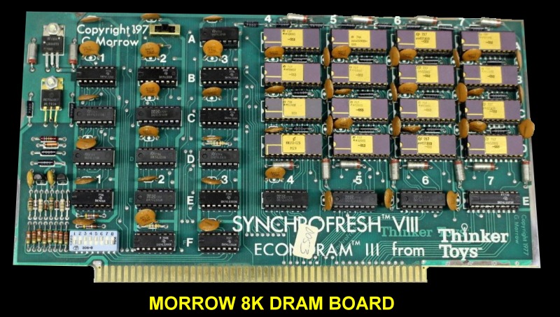
The Thinker Toys "Synchrofresh" 8K memory unit was an early DRAM S-100
board. It contained two completely independent 4K blocks. Each of these two
4K blocks could be placed on any 4K address boundary.
At the top of the circuit board just above position 2A, there is a
three-position slide switch. The left and middle positions are both write
enable states while the right position is the write protect state.
When the board is to be used as read/write memory, the slide switch should
be to the left or in the center. In these positions, the CPU can write into
or read from either 4K memory block. When the unit is to be used as "read
only" memory, the slide switch should be in the right most position. In this
position, write commands issued to the memory by the CPU or DMA devices are
ignored. The write protect mode is especially useful when it is necessary to
prevent a program or data from being accidently destroyed by another program
or from the front panel.
Addresses to the memory from the S-100 buss and the refresh address counter
are buffered and selected through three 74lS157/158/257/258 quad two-input
multiplexors. The control input to the multiplexors comes from a D-flip-flop
which switches data and refresh addresses to the array at the proper times.
A careful examination of the timing of this flip-flop will reveal that
addresses are switched in the middle of a memory cycle. This would be
unacceptable were we using static RAMs. The situation with dynamic RAMs is
somewhat different. The address inputs of a dynamic RAM chip are not only
buffered but also latched. This latching occurs with the rising edge of
CENBL (see manual below), the signal which initiates a cycle for the memory
chip. The main concern with the address signals to the 2107B is that they
are stable at the rising edge of CENBl and remain so for app rox imate Iy
150 ns.· In the present case, the MUX CNTL signal does not change for 250 ns
after the rising edge of CENBl, giving a margin of 100 ns.
The manual for this board can be
obtained
here.


