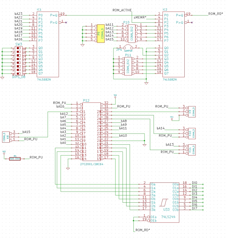
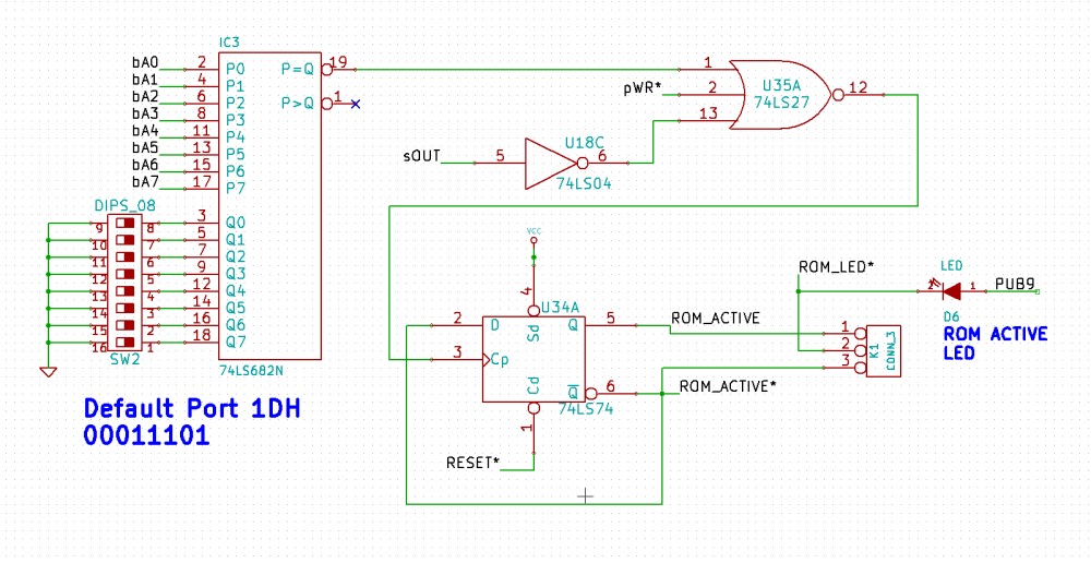
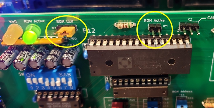
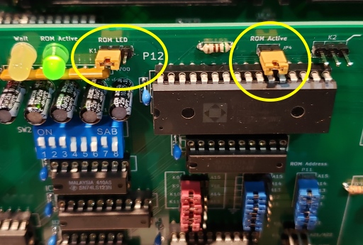
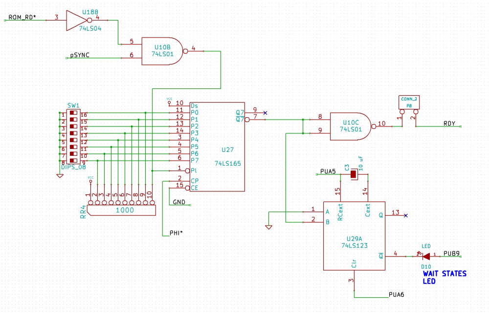
| |
| P1 |
Size |
Address |
Type |
K8 |
K9 |
K10 |
K11 |
P9,P10 |
P11 |
SW3 |
|
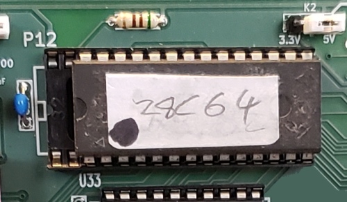
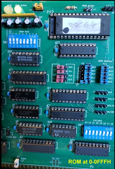
28C64 |
4K |
0000H-0FFFH |
EEPROM |
1-2 |
1-2 |
1-2 |
1-2 |
A15,close
A14,close
A13,close
A12,close
A11-P9,1 |
A15,close
A14,close
A13,close
A12,Close
A11,Close |
All
Closed |
|
28C64 |
2K |
0000H-03FFH |
EEPROM |
1-2 |
1-2 |
1-2 |
1-2 |
A15,close
A14,close
A13,close
A12,close
A11,close |
A15,close
A14,close
A13,close
A12,Close
A11,Close |
All
Closed |
|
28C64 |
2K |
8000H-87FFH |
EEPROM |
1-2 |
1-2 |
1-2 |
1-2 |
A15,close
A14,close
A13,close
A12,close
A11,close |
A15,Open
A14,Close
A13,Close
A12,Close
A11,Close |
All
Closed |
|
28C64 |
2K |
E000H-E7FFH |
EEPROM |
1-2 |
1-2 |
1-2 |
1-2 |
A15,close
A14,close
A13,close
A12,close
A11,close |
A15,Open
A14,Open
A13,Open
A12,Close
A11,Close |
All
Closed |
|
28C64 |
8K |
C000H-DFFFH |
EEPROM |
1-2 |
1-2 |
1-2 |
1-2 |
A15,close
A14,close
A13,close
A12,P9,2
A11,P9,1 |
A15,Open
A14,Open
A13,Close
A12,Close
A11,Close |
All
Closed |
|
28C64 |
2K |
D000-D7FFH |
EEPROM |
1-2 |
1-2 |
1-2 |
1-2 |
A15,close
A14,close
A13,close
A12,close
A11,close |
A15,Open
A14,Open
A13,Close
A12,Open
A11,Close |
All
Closed |
|
 |