Introduction to the 8MB Mezzanine RAM mini-Boards
Our 16MG Static RAM
board turned out to be a great success. The board was fast and could handle 8 and 16 bit data paths 100% reliably with all the CPU's I could throw at it. It reliably runs with our
Z80,
6502,
8088,
8086,
80286,
68000
and 80386
CPU boards. I have not found a vintage S100 CPU board that would not work with it.
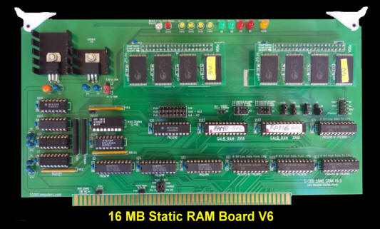
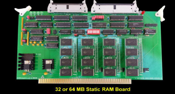
Here is a picture of the board -- as well as a 32MB RAM board (see below).
The actual static RAM chips used with these boards are the Cypress 2MB X 8 (CY62167's). They come in two formats, the
CY62167E
which run with a Vcc voltage of 5 Volts and a
CY6216DV30 which runs with a Vcc of 3.5 Volts. Both are available from a number of venders -- though there is a wide price range. The 5 Volt units
(which I prefer -- in my hands are more heat resistant) are a little more expensive. I get mine from
Arrow Electronics (CY62167ELL-45ZXI). They are not cheap ~$10 each. So it will cost you about $80
in RAM chips to completely fill your S100 bus system with this board. Not bad
when you remember that once upon a time you paid that for 1K of RAM!
The boards utilized two "mezzanine mini-boards" that hold the actual
SMD RAM chips. SMD chips had to be used because nobody makes a 2M X 8 static RAM chips in a DIP chip format. In line with current trends, all new high capacity static RAM chips are in a surface mount format.
These same mezzanine RAM mini-boards are used with out
OTT
32MB RAM boards for used with our
80386 (and 80486)
CPU boards.
The only problem is soldering on the SMD RAM chips to the mezzanine boards.
There are four RAM chips per boards. I have done a number of these
boards and have always found it a challenge, sometimes ending up with a dead RAM
chip -- due to either a bad solder joint or an over-heated RAM chip. I
concluded that the main problem was the solder pads on the "V06c" mezzanine
boards were too small. What is needed are longer horizontal pads which can
be layered with solder and then one only has to touch each RAM chip pin briefly
to have it fuse with the solder below it.
A new "V06d" mezzanine RAM mini-board is presented here along with more details
as to how to solder the RAM chips to these boards and check them out.
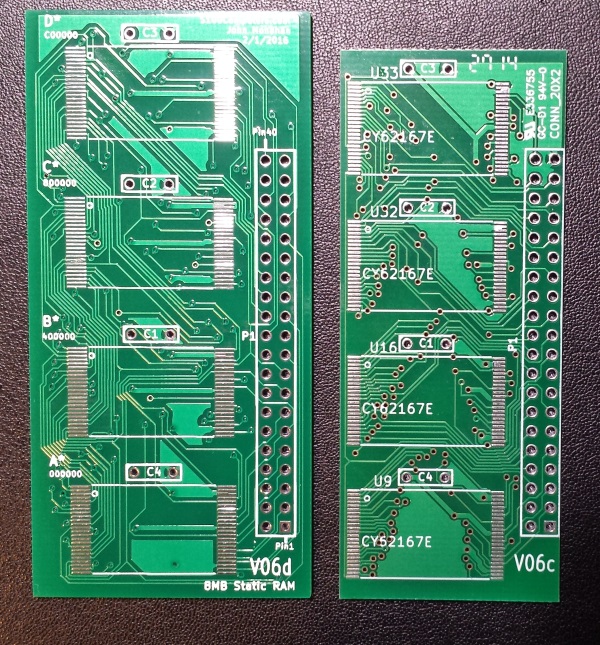
First here is a picture of the old and new mezzanine boards.
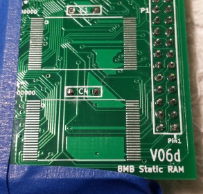
You can immediately see that the V06d boards are slightly larger, but more
importantly the RAM solder pads are wider.
SOLDERING SURFACE MOUNT RAM CHIPS
Everybody seems to have their own way to solder SMD chips by hand. There
are many excellent videos on the web outlying various procedures.
I found this
U-Tube
video
helpful.
Step by Step.....
Use a very fine tip 10-15W soldering iron.
The tip must be small enough not to bridge more than two RAM chip pins.
With a small brush cover the board solder pads with solder paste (I use,
"DeoxIT Rosin Soldering Flux").
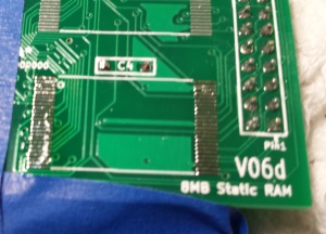
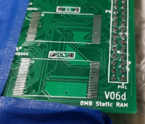
Here is a before and after flux application.
Then "slop" solder on all the pads evenly. Run the iron down the pads. The
flux will prevent pad solder bridges. When done each pad should have a mound of
solder on it but not so much as to bridge across to the next pad. Then remove
the excess flux with flux remover spray. ( I use "Fux Wash" by DeoxIT).
Blow air over the board to completely dry it. Do not touch the pads with
your fingers. Here is a picture of the prepped board.
Its not very clear in the picture but each pad has a layer of solder on it
evenly spread.
Next add a little solder flux again. Very little is required -- just a thin
film.
Carefully align pin one on the circuit board pad so the visible pad is
equal on both sides of the chip. (i.e. the chip is exactly centered).
Press down on the chip and touch the solder pad for pin 1 with the soldering iron. If it is clean no
actual solder is required.
There is sufficient solder on the board and chip to make a connection.
Next go to pin 25. Carefully align the chip so all pins are exactly over the
circuit board pads and solder exactly as for pin one.
Its critical to have careful alignment of the pins with the pads. Before
soldering check the opposite diagonal chip pins are not off.
I have found the easiest way to aligned pin 25 is to place a blade at the side of
the chip and twist the blade slightly. This very slightly moves the chip.
Next with your very fine tip soldering iron touch the solder on each pad and
scoop it towards the RAM chip pin all the time pressing down on the RAM chip
with your finger. Do not over solder. The mere melting of the solder is
actually sufficient for a good pin contact. If you feel the RAM chip getting
hot stop immediately and let it cool. I have found these chips do not tolerate
overheating well. I usually stop after 5 pins for a few seconds to let things
cool. I cannot stress enough that the slightest melting of the solder on the pad
is all that is required.
When done remove the excess flux with flux remover spray. Blow air over the
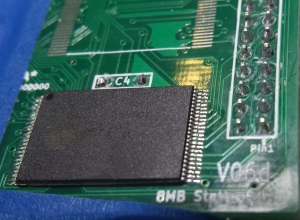
board to completely dry it. Here is a picture of a RAM chip soldered as
described above.
It should not be necessary, but just to be safe, with a magnifying glass carefully examine each pin for cross bridges.
If found, remove with solder wick.
I have recently started to use a headgear unit that contains a light and
binocular magnifying glass. Jewelers use them, there are many on the web.
Looks geeky but it really helps with the above.
DEBUGGING
These boards contain a lot of RAM. If you are using them for a Z80 (64K
RAM) chances are you will not have a "bad patch". You just have to have
the lowest region of the RAM working. In order to test/debug a board it is
useful to understand how the RAM on this boards is arranged.
For 16MB RAM board (all versions), one mezzanine board addresses even bytes
(connector P104), in the S100 bus address space, the other odd bytes
(connector P103). This means that this board would never
work correctly with only one mezzanine board.
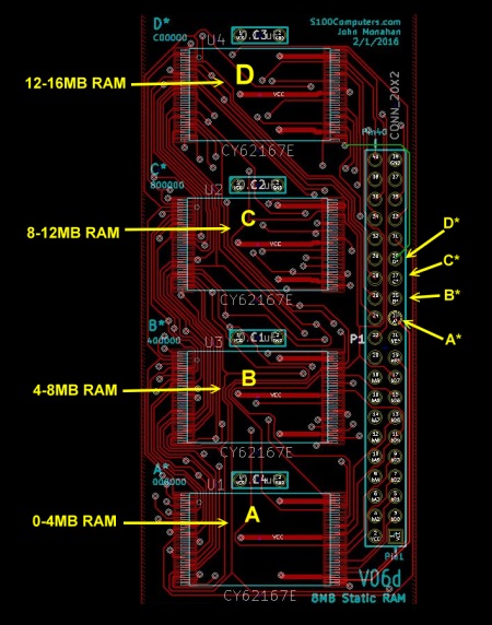
Next on each mezzanine board there are 4 chips. The individual chips are
addressed (using address lines A22 & A23) as shown here:-
What this means is that the most critical chip is the bottom chip beside pin 1
of the boards connector. To get started you should solder one RAM
chip in this position on two mezzanine boards. Insert them in your system
and see if you can boot up your Z80 monitor. If not, check for solder
bridges and/or with a fine blade/needle see if any of the RAM chip pins move on
the board. Re-solder and retry. Do not go forward until the problem
is solved. If need be, remove the chip with a heat gun and try another.
Sometimes it helps to place a little solder flux on the RAM pins before
resoldering. Be sure to remove it with flux remover however before powering up
your system.
Next see if you can boot a banked version CPM3 (which uses RAM above 64K).
Next see if you can boot the 8086 monitor and MSDOS. If this works you
probably have a good lower 1MB of RAM.
The real test comes with the extensive tests in the 80386 (protected mode)
monitor.
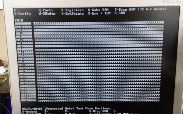
First do a memory map ("A" command). It should appear like this:-
Then use the protect mode "J" command, option 7, to check RAM from 100000H to
3FFFFFH.
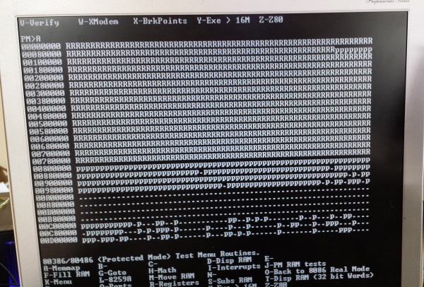
If all is well insert the second RAM chip (B) on the pair or
mezzanine boards. Repeat the above tests. The memory map should now
look like this:-
Don't worry about RAM above 7FFFFH. Noise on the bus will give various
configurations.
Then use the protect mode "J" command, option 7, to check RAM from 100000H to
7FFFFFH. If all is well insert the third and fourth RAM chips (C & D) on the
pair or mezzanine boards. Repeat the above tests. Then do a complete
16MB 80386 RAM test using the "J" command, menu #4. Here is a
picture of a checked out board result:-
For the
32MB
RAM OTT board (all versions), the addressing is different. The 4
vertical mezzanine boards address bytes 0, 1, 2 and the 3 respectively. So
to test RAM you will need 4 mezzanine boards. Again one chip per board is
fine to start with. Sometimes its easier to check the mezzanine boards in
a 16MB board first before popping them into a 32MB board.
Bugs and Notes
I have not found any bugs in
this board so far, however they do not fit well in the very first (V1) 16MB RAM
board. They are a little too wide and overlap each other in the board. The work
fine, just not a neat arrangement. They fit fine in the V5 & V6 boards.
Also if you are on a tight budget, you need only add
the first RAM chip to both mezzanine boards yielding an S100 bus system with 4MB
of RAM.
A Production V06d Mezzanine Board
Realizing that a number of people might want to utilize a
board like this together with a group of
people on the
Google
Groups S100Computers Forum, "group purchases" are made from time to time.
Please see
here for more
information.
Please note if you have V06c mezzanine mini-boards they are perfectly fine. The
circuit is identical to that on the V06d boards. Only the RAM pin pads
size are different.
The soldering approach is exactly the same.
MOST
CURRENT 8 MB MEZZ BOARD SCHEMATIC
(V06d 3/21/2016)
MOST
CURRENT 8 MB MEZZ BOARD KiCAD Files
(V06d 3/21/2016)
V6d Mezzanine KiCAD files (V06d,
Final 4/1/2017)
Other pages describing my S-100 hardware and software.
Please click
here to continue...
This page was last modified
on 11/30/2017


