S100 Computers

Home S-100 Boards History New Boards Software Boards For Sale
Forum Other Web Sites News Index    
 
Intersystems Series II Z80 CPU Card.
 
 
This was Ithaca Audio's (later known a Intersystems) second Z80 CPU card.

Intersystems Z80 CPU-II Board

The card was designed to be IEEE 696 compatible. The card was sold as a kit.  It have an onboard ROM allowing a monitor boot directly from the board.  It also had on board complete circuitry for an AMD 9519 interrupt controller.
 
The Intersystems Series II Z-80 board was one of the first S-100 processor boards to take full advantage of the IEEE specification,. It has many special features  that made it both powerful and easy to use.    

Among  these features were:-
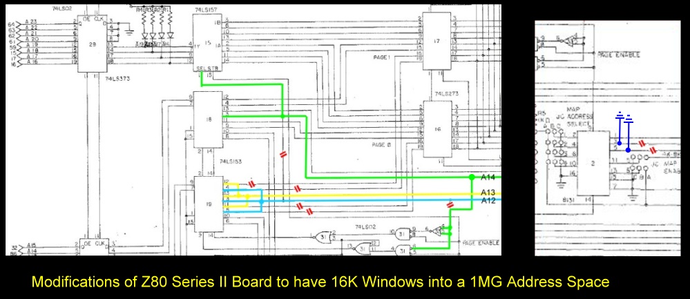
  A simple address management system that provided two 1 Kilobyte segments reloadable anywhere in the first megabyte of the 16 megabytes of the S-100 address apace. Four light-emitting-diodes Indicate the four most-significant  address bits.
  A Vectored   Interrupt   Controller   that provided sophisticated, high   speed interrupt   handling   with   individual   masking,  fixed   or   rotating priorities, and optional  polled operation.
  2 or 4 MHz processor speed  which was on-board pin-jumper selectable.
  PROM monitor socket will accept 2708, 2716, 2759, or 2732 EPROM's and a reset jump is provided to the PROM.
  The PROM may be addressed at  any 1 K boundary in the 64 K address space.
  On-board wait generator optionally adds a single wait state to any Instruction Fetch, Memory Reference, Input/Output Reference, or on-board PROM Reference.
  On-board circuit conducts the IEEE specified nested bus transfer for glitch-free DMA operations, and DMA controllers need not duplicate the circuit.
  Special engineering features included 2 self-test modes for quick circuit debugging and Address and Status latching to reduce bus noise and  improve  reliability.

Extended Addressing with the IA-Z80 Card
One very unique feature of this Z80 card -- and the reason I like it so much --  is that the card has the ability for the Z80 CPU to adderss RAM addresses greater than 64K.   This is done by a simple trick of using IC's 15,18 & 19 (74LS157's) to latch/translate addresses A12 to A19 before each RAM read or write signal.

This address translator" is configured as an 8K "window" in the normal Z80 64K address space. The location of the window (actually two 4K windows, see below) is set by on board jumpers (JC 1-6). To address this translation window function you output a byte to an on board port set with jumper JB (1-6).  I use port D2H for the lower 4K window, and D3H for the next higher 4K window.  On reset, the window is set to 0K and 4K and so overlaps with normal RAM. So the window is transparent to the system. By outputting values to ports D2H and D3H you can map these windows anywhere in a 1MG address space.  

Useful, but only 4K or 8K blocks!  For a CPM3 system to be practical in its bank select mode it would really be nice to have 16K windows. A friend of mine Geoff Shapiro back in the 80's noticed that the board could be easily modified to allow a 16K/32K window.  What we do is alter some of the address lines going into the 74LS157's. I will describe this in detail as it really makes the board ideally suited to running CPM3 in banked mode.  You can probably do this by bending up pins and wire wrapping them. Since I regard it as permanent in my system I cut board traces.

Cut the board traces to pins 3 & 5 of U2. Connect the pins to ground. 
Cut the board trace to pin 1 of U15 and connect the pin to A14 of the Z80 (pin 4, find a nearby trace).  
Note the trace from pin 1 of U15 starts out under the IC socket and travels across the space between it and the socket for U16. To cut it you can (in some cases) lift the socket and see it or with a ohm/conductivity meter on pin 1 scratch the tarce traveling across to under socket U16. It is the top most trace between the two sockets under the "U" of U15 on the silk screen.
Cut the board trace to pin 6 of U31 and pins 4 and 5 of U33 and connect the pin to the (now free) three pins together.
Connect these three pins to A14 of the Z80 (pin 4, find a nearby trace).  
Cut the board trace to pins 4,5,11 and 12  of U19.  Connect pins 11 and 12 to pin 13 of U19. 
Connect pins 4 and 5 to pin 3 of U19.
For Jumper JC, All jumpers (1-6) should be B-C.


The schematic with these modifications is shown below. See here for the IA-Series II original schematic.

IA-Series II Modifications 

You now have 16K window capability. Let me explain:-

Suppose you wish to address RAM at 000F8000H to 000FFFFFH (the top 16K of the 1MG address space of the 8086). With these modifications you output to port D2H (in my case), 0F8H  and you output to port D3H, 0FCH.  Now when you display 0,7FFF you will actually see 000F8000H to 000FFFFFH.  The two back to back 16K windows translate the 16 bit address lines into 20 bit address lines. This makes writing CPM3 to address >64K RAM space very easy and efficient.  Remember to reset the windows back when done (or hit reset). 

The relevance of this is that it allows you to see the ROM code you may have for a 8086/80286 in high memory with a Z80.  As I will describe when I talk about my S100 8086 or 80286 board, I can relocate in RAM (with my Z80 monitor)  the code at  000FC000H -000FFFFFH to 0H-3FFFH by outputting to port D2H the following:-

QD2,FC

Now RAM at 0-3FFFH shows the actual memory at 000FC000H to 000FFFFFH

If we put at the 8086/80286 reset address (000FFFF0) or 3FFFH in RAM the following code the test code:-

 B0,33,E6,01,EB,FA

When the 8086/80286 resets it will output to may SD Systems Video board (port 01H) the letter "3" continuously on my LCD/CRT  --  when it gets control of the bus for the first time. A simple basic test for the board.

This is a bit difficult to understand. Let me try it again...

This is how we do this. With the above modifications to the board, using the monitor we switch the Z80 window of the 8K block of RAM from 0000H - 3FFFH to FC000H - FFFFFH,  (assuming you have a 24 address bit RAM board in the top 1 MG of RAM).  We do this by:-

QO
D2,FC

Then we deposit the above 6 bytes in RAM at 3FF0H in RAM

S,3FF0,B0
S,3FF1,33
S,3FF2,E6
S,3FF3,E6
S,3FF4,01
S,3FF5,EB
S,3FF6,FA


Then if you activate your 8086 or 80286, it will find the code there on reset.
We could just as easily entered

QO D3,FC
and
S,7FF0,B0
S,7FF1,33 
etc.

Here are some more examples to explain the translation system

S100 Address lines
A19 A18 A17 A16 A15 A14 A13 A12 A11 A10 A9 A8 A7 A6 A5 A4 A3 A2 A1 A0
  7   6   5        2                             
Port 0D2H

Examples:-
Address 0000 0000H + Port D2H = FCH         translates to an address of 000F C000 0000H
Address 0000 0000H + Port D2H = 10H         translates to an address of 0001 0000 0000H
Address 0000 0000H + Port D2H = 14H         translates to an address of 0001 4000 0000H
Address 0000 1000H + Port D2H = 14H         translates to an address of 0001 4000 1000H

Disabling the Onboard PROM of a IA-Z80 Card
The second modification I made to this board was to allow the disabling of the on-board EPROM under software control. Without this the EPROM will appear in each 64K segment of memory. In may case at 0F000H-0FFFFH, 1F000H-1FFFFH, 2F000H-2FFFFH.... Particularly useful is the ability to remove the EPROM from the first 64K of RAM allowing a 64K CPM3 system.
 
To accomplish this we take advantage of the fact that the above 16K window mapping frees up bits 0 and 1 of ports D2H and D3H (or whatever address you have yours jumpered to by Jumper JD).  If we cut the board trace of pin 14 of U1 (going to jumper JB of (A-B-C) and connect a wire from pin 14 of U1 to pin 19 of U17 (data line 0) we can disable the EPROM anytime we output to port D3 with bit 0 equal to 1. So in our example above if we output to D3H 0F9H we will relocate the RAM window and remove the EPROM addressability from the board. Note you cannot do this from your monitor in ROM because you will have removed the next op-code the Z80 would receive. 

To test, recompile the Z80 monitor to say 8000H, load it with ZSID, jump  to 8000H and then output to the D3H port.

16 Bit Port Addressing
The current Z80-Series II  board outputs all I/O port address on the high (A8-A15) and low 8 bit (A0-A7) address lines.  Most early S-100 Z80 boards did this to be compatible with the original 8080 CPU which did the same thing.  Actually few if any S-100 I/O boards utilized these high bits. Because all 8 bit CPU's had a maximum of only 256 ports this was never a problem.

With the introduction of 16 bit systems and the I/O port range now extended to 64,000 ports (i.e. 16 bits), it became relevant if you wanted to address ports greater than 256 to have 16 bit I/O addressability on the bus.  The good news is it is easy to modify the Z80 Series-II CPU board such that the upper I/O address lines are zero. In other words the I/O address range is 0000H to 00FFH.

To accomplish this cut the board traces of pins 6 & 10 of U19 and pins 6 & 10 of U20 (a 74LS157 and 74LS153). 
Jumper with a wire all 4 chip pins to ground.

You are done. Now anytime you output to an S-100 port with the Z80 the upper address lines will be zero. This avoids messing up ports that say an 8086 would address.

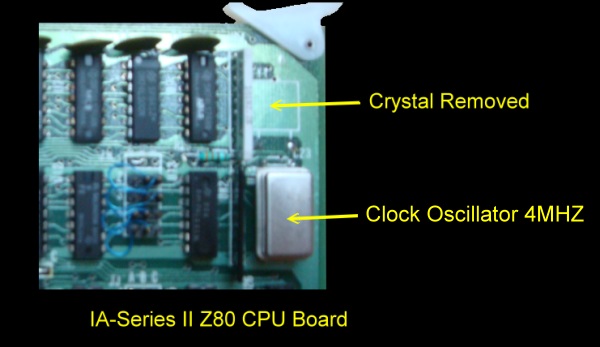
Modifying the Board Clock Signal.
If you find yourself changing the main S-100 clock frequency on the board a lot as you experiment with other S100 boards (e.g. a slave CPU board) it is nice to be able to do this quickly.  I removed the older clock circuitry on the board utilizing U14 (a 74LS124) and a 8MHZ crystal) and put in place a self contained clock oscillator generator "chip".  These are very common now and provide rock solid stable square wave outputs. They have only 4 pins, (ground, +5V and output). To accomplish this..

Remove U14, cut all traces to pins 1,7 and 10. Insert a 14 pin oscillator with its pin 1 in pin 1 of U14 (pins 8 & 9 are now free). Jumper U14 pins 7 & 8,  and connect U14 pin 9, (8 of oscillator, frequency output) to the trace going to jumper JG pin B .
Remove the crystal its no longer needed. Remember the clock oscillator in the top section of socket U14 (i.e. a 14 pin IC in a 16 pin socket, so pins 8 & 9 are free).

You are done. Now to switch frequencies simply plug in the appropriate frequency generator.  I normally start with a 4MHZ system.
The picture below shows my system.

Frequency Generator

Note if you run this board at anything other than 4MHZ you need to bend out pin 7 of U37 which supplies the bus standard 2MHZ clock signal used by a few older S-100 serial I/O boards.  As we shall see when I get to my front panel board I generate the 2MHZ signal on that board.

Intersystems provided the ability to generate S-100 adders "Full Latched" and "Partial Latched" address lines.  The former were S-100 signals exactly as defined in the IEEE-696 specs., where the bus address lines are stable from early in BS1 to BS3 (i.e. .over the total range). In the partial latch mode the address lines don't quite make it through all of BS3.  However the latter case allows the board to get to higher speeds.  With all boards I have used I have found the partial latch mode to work fine.  For those interested here are the timing diagrams.
IZ Z80 Latch Modes
Here is a logic probe tarce of my board. I put 76H in RAM at 0H and jump to that location. This puts the Z80 into a HALT state. You can see that the pDBIN strobe is nicely going from high to low while the address lines are stable.

Logic Diagram HLT ot 0H

Next to, look at I/O signals. I put into RAM at 0H:-

DB 00 C3 00 00

This will input from port 0H continously.  Here is the corrosponding S-100 signal analysis.

Logic analysis of I/O signals

Again you can see that the pDBIN goes from high to low well before the address lines change.  The same data can be seen for memory and port writes.

This Z80 board also has a great interrupt controller chip, a AMD 9519. This chip when combined with the Z80 provides an enormous amount of flexibility in handling S-100 interrupts. It's ideally setup for multi-user situations. Its a little complex to setup but the manual supplies all you need to know with good examples. However if you use a multiprocessor S-100 system you are better off having the interrupt controller on another board. I only use interrupts in my 16 bit systems so I do not utilize it with this board.  Also the chip runs hot! You can almost fry eggs on it! Normally I remove the chip from the board.
 
The manual for this card can be downloaded here.  See here for more discussions about this board.

Other InterSystems S-100 Boards
64K Dynamic RAM    8K RAM   EPROM   IA-Display   FDC   IO-Card    Z80-Series-II    Z80   ADDA Board   EPROM Burner 
FPB   256K Dynamic RAM   16-64K EPROM  HDA   Z80-Series_III  6SIO  EPROM Emulator  RTC Board


This page was last modified on 10/25/2013