S100 banner
Home S-100 Boards History New Boards Software Boards For Sale
Forum Other Web Sites News Index    

The S-100 Bus FPGA 80486 SBC Board.
  FPGA_80486
This is one of the more complex S100 boards I have fabricated.  It took over 6 months to complete.  It is a four layer board. This board is not recommended for beginners.
There is almost a limitless amount of software that can be written for this board. While a very extensive ROM monitor is included (for both Real mode and Protected mode), several sections remain to be written. These include:-
1.    Modifying the IDE/CF card BIOS to work with the onboard SD cards to run MSDOS V4.01.
2.    Add 16 bit data transfers for the lower 64K S100 bus RAM "window".  Currently that RAM is only 8 bits.  (The remaining 16MB of RAM is of course 32 bits wide).
3.    Modify the FPGA code to run the board as a bus master.


Introduction
The original S100 bus 80486 board has proven to be a very reliable board.  If you are not familiar with that board it is essential you read up on the 80486 Board before going any further here.  Much of what is written here assumes you are familiar with that board.  There are also  introductions to FPGAs and how to program and use them described here.

We will now move things up a notch and use the full power of the Cyclone IV FPGA to make a 80484 CPU board with many onboard functions. We will construct and program the FPGA to be a S100 Bus 80486 CPU "Single Board Computer" (SBC) board somewhat similar to our earlier S100 bus Z80 FPGA SBC and 80286 FPGA CPU boards. 

The board contains:-
A "real' 80486 CPU running at 16mHz (or greater).
The board has 16MB of onboard 32 bit wide fast static RAM that is addressable locally to the 80486
A CPU carve out "window" to the S100 bus RAM - variable from (0K to 16MB) is provided running at 8mHz.
An onboard 128K EE-PROM containing the 80486 monitor along with diagnostics support for the SD cards, an IDE/CF card and the ZFDC Floppy disk controller.
The 8 bit wide ROM is transferred to the 32 bit wide onboard RAM upon startup and removed from the CPU's address space
An IBM PC PS2 keyboard input port (with input converted to standard ASCII)
A USB serial I/O port at speeds up to 38K to a PC
Two SD Micro Card slots and an interface to boot MSDOS V4.01
There is an FPGA interface to an onboard SPI DS1305 clock/calendar RTC chip with battery backup.
A 4 bit IOBYTE input software port and 3 status LEDs.

While this board internally is quite complex,  externally it looks and behaves fairly simple. This can be part of a simple stand alone S100 bus system since with this board alone and a simple USB/FPGA programmer they can have a complete S100 bus MSDOS system. Then gradually the user can inactivate various sections within the FPGA code and activate the corresponding old/new S100 boards they have in their system. They can start off by looking upon the FPGA as a black box.  

Keeping in mind the above potential audience, I will try and over-explain some things below.  Our "hard core" audience can just skip ahead.  That said,  this is NOT a board for a complete electronic novice. Minimally you should have some soldering experience and knowledge of electronic circuits.  You should for example be comfortable with web sites that describe Arduino or Raspberry circuits.  You should have a basic understanding what a Field Programmable Gated Array (FPGA) is. If not, look them up on web.  In summary, these chips allow you to lay down any circuit you might come up with within the FPGA chip just like you might do by soldering hundreds of TTL/74xxx chips together as in the old days.  Its all done in software. The resulting code/pattern is then programmed into the chip.

For those more electronically sophisticated... I looked at using an internal 80486 FPGA simulator.  I could not find a free one in the public domain.  There is an nice 80186 FPGA simulator by Jamie Iles but unfortunately the code was too complex/convoluted for me to use.  Also the 80186 has defined I/O ports for its support components that often conflict with other S100 board hardware. 

The choice of 80486 CPU is quite important, in order to avoid the need for 5V voltage level shifters for the FPGA we will use the 3.3V AMD 80486 CPU.  This way the 80486 CPU can directly interface with the FPGA GPIO pins.  The board will not work with the older/slower 5V 80486 CPU's.

Finally I would like to point out that while the chip density on the board is not too bad,  the routing to the chip pins is very dense.  It took a 4 layer board to fit everything. Even with that, Freerouter took up to 24 hours to get a reasonable solution.


What Is Needed
The FPGA we will use here is an Altera/Intel Cyclone IV FPGA.  This chip is currently in about the middle range of the programming capacity of FPGA's.   The actual chip uses a "Ball Grid Array" method of soldering it to a printed circuit board.  This requires some specialized equipment, so normally one purchases an "adaptor board" for these chips with the chip on it.  Besides providing "normal" pin attachments to (in our case), the main S100 board,  these adaptors contain a number of voltage regulators, Flash RAM, a programming socket  and other components these FPGAs require to operate.

As for our previous boards we will use the WaveShare "CoreE4CE10" Cyclone IV board adaptor. Its schematic can be seen here.
    
  CoreEP4CE USB Blaster  
        
The second thing you will need is a device to program the FPGA chip itself. 
There are many FPGA programmers available. I really like the USB Blaster (V2) that Waveshare sells.  Its simple and reliable.  And importantly, works directly within Intel's Quartus V12 (see below). You will also need an EEPROM burner for the onboard EEPROM. I like the Wellon burners.

Somewhat unexpectedly you will need to pay particular attention to the special very tightly spaced pins on the above adaptor board.  Because there are so many FPGA output pins, its not practical to have a connector with the standard PC board 0.1" pin spacing.  The above WaveShare unit uses unusual 2 mm dual row pin connectors.  Unlike to normal 0.1" connectors these are quite rare an expensive.  If you solder these female sockets to the board the WaveShare adaptor sits quite high on the board and will prevent the next S100 bus slot from being used.  If you carefully remove the JTAG socket top border edge with a wire cutter - all around about 1/8", it will fit into most S100 bus motherboards without taking up two slots. Alternatively you can solder the adaptor directly to the S100 board. Of course removing the adaptor is all but impossible in this case. 

Please note the 2 mm dual row pin connectors (Digi-Key #1212-30-ND sockets) for the WaveShare adaptor are quite tricky to fit on to the board.  I found the best way to do this (after trimming them to pin size), is to push them half way on to the adaptor pins and then wiggle them to fit the whole unit on to the S100 board.  Figure on spending 10 minutes on this step!  Do not solder them to the board first and then try and press the adaptor down on them. They are very fragile and internally the leaves will bend if socket angles are not exactly correct.  When in place, check each pin is visible on the back of the board before soldering.  Only then solder all around.  Add as little solder to each pin as possible - the narrow pins have a tendency to wick up solder internally.  I find it best to have the socket base slightly above the front board surface when soldering in the first two pins. Wedge a sheet of thick paper between the socket and the board initially. Better sockets are the Mouser
#437-8338703810001101 38 pin sockets (carefully clipped to size). However these sockets are often out of stock at Mouser

The rest of the boards components are standard -- available from Jameco, Mouser, Digi-Key etc. For prototype boards I generally use "double swipe" IC sockets. For a critical board like this I prefer to use "Machine Tooled" IC sockets.  However they are more expensive and you have to be particularly careful not to bend the actual IC pins. 

  
Quartus Prime.
For Altera/Intel FPGA's the program of choice to program them is called Quartus Prime.  This a very large Windows based IDE interface. It is completely self contained with everything you need to write FPGA code and program the chips. Its an expensive software package. Fortunately Intel supplies a "Quartus Lite" free version for students and people like us.  Even this is way overkill for our use.  The most recent version can be downloaded from this Intel site.  The package will take ~20 minutes to install on Windows 10.  You may want to first review this video about the installing process. Please see the Notes section at the bottom of this page for more help installing Quartus.
 
Please keep in mind that programming an FPGA is different from the normal linear/sequential programming approach you may be used to.  On an FPGA everything is potentially happening at once.  Good FPGA programmers take years to excel and currently are in high demand.   Timing and power distributions across the chip almost become an art form.  Fortunately out needs will be far simpler.   Also there seems to be an excellent community of experienced people ready to help -- beginners.  I have found the Intel FPGA Forum to be very useful and helpful.   However by far the best way to get started is to look at a few YouTube demonstrations.   

One outstanding YouTube video to get you going with Block Design File FPGA programming is this one by ClockFabrick Electronics Academy
Note, click on the "full screen icon" for easy viewing. Use ESC to return.   
Also please allow a few minutes for it to download.  It's a very large (50 minutes) video file.


For absolute FPGA beginners, rest assured,  you can more or less use the FPGA code examples below as "Black boxes" to get this board up and running. However you will be missing one major aspect of the board. By stepping along and understanding how the FPGA code works you will in the end have the ability to modify the board in amazing ways.


Prerequisites for Testing and Usage of the FPGA 80486 board
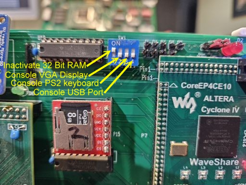
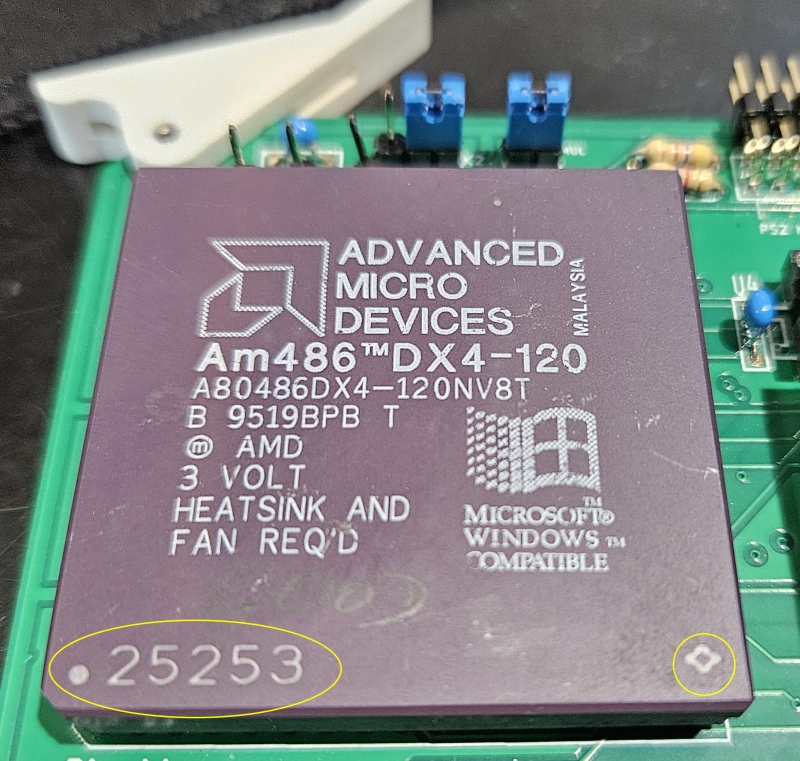
The FPGA 80486 board, when completed following the build instructions below, will function as a slave CPU. Therefore while building and testing this board you must have the following boards installed in your system:-

1. Either the "Z80 Master CPU board", "Z80 SBC board", or "Z80 FPGA SBC board". The instructions below assume you are using the "Z80 Master CPU board". If you have one of the Z80 "SBC" boards the monitor program on those boards lacks an "O" command to perform a swap to the 80486 slave CPU, and you will need to use the monitor to manually perform an Input from port EDH to initiate the processor swap (QIED).
The System Monitor board needs to be present for when an input from its port
EDH lowers the TMA0 S100 bus line.  P30 3-4 must be jumpered. Without the System Monitor board you can "force" this FPGA_80486 board to slave mode by jumpering P30 1-2 and K5 1-2.  Remember TMA0 must be low for this board to take control of the bus.


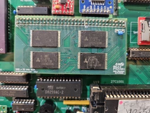
2. An S100 RAM board with a minimum of 64K, which will already be installed in your system if you are using the "Z80 Master CPU board". If you are using one of the Z80 "SBC" boards and their on-board RAM, you will need to install an additional separate S100 RAM board with at least 64K.

3. Having a "Propellor Console Board" installed in your system is not essential, but it will make the initial build steps of the FPGA 80486 board much easier. If your system does not have a "Propellor Console Board" you will be unable to communicate with the FPGA 80486 board until after the USB serial port interface has been installed, several steps into the build process. Alternatively see if you have a console IO interface that can be configured like the Propellor Console Board (Status Port 0. Data Port 1) and the same status bits you could use it.

4. During initial building and testing of the 80486 FPGA board, it is recommended all boards be removed from your system with the exception of the three boards listed above. If your system has an S100 Bus SMB and/or Bus Display Board installed - those boards can be left in place.

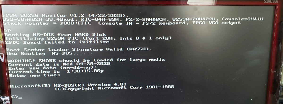
5. At the step below "The RTC Circuit" your 80486 board will be ready to boot MSDOS. A "CF/IDE board" will need to be installed in your system at this point, allowing you to boot MSDOS from card "B" on the CF/IDE board. Note that (a) the FPGA 80486 board cannot boot MSDOS from the CF card on either of the Z80 SBC boards and (b) since software support for the SD cards on this FPGA 80486 board is incomplete.

6. This FPGA 80486 board has most of the key functions of the MSDOS Support board built in, so a separate MSDOS support board is not required to run MSDOS.

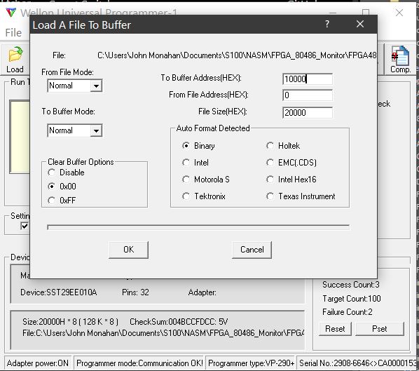
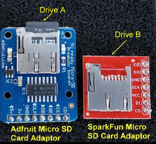
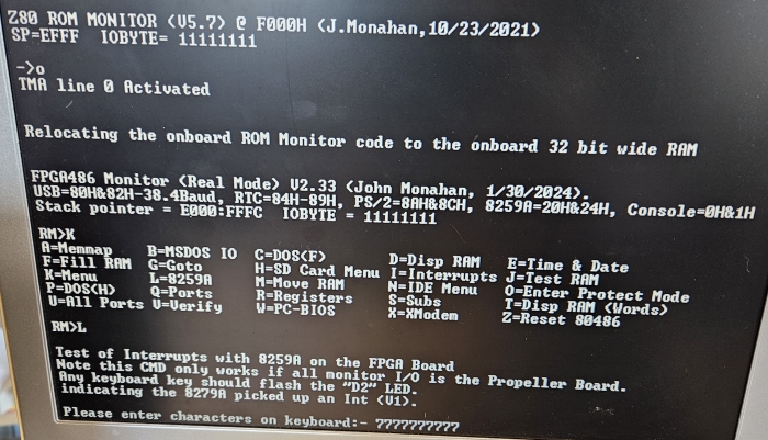
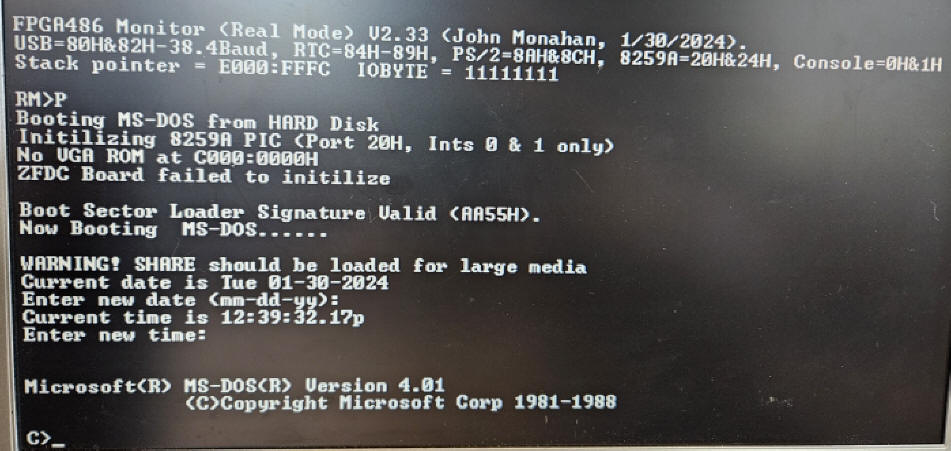
7. Currently software to boot MSDOS from either of its on-board SD cards is not written.  You need to use the IDE/CF card board.  The MSDOS card must be in drive B: (A: is always for CPM3).  MSDOS can be downloaded from here.

8.  It is recomended you place your S100 bus RAM board next to this board in the bus.


Step By Step Building the FPGA 80486 SBC Board
The build instructions are fairly simple for this board but because it is a complex board building it should not be rushed.  As always, first examine the bare board carefully for scratches or damaged traces, use a magnifying glass if need be.  A broken trace is almost impossible to detect by eye on a completed board.
   
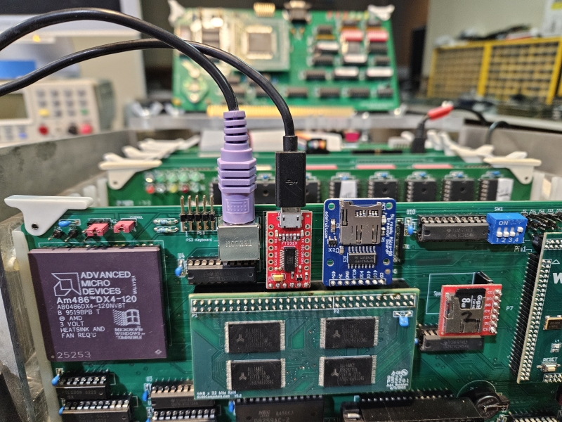
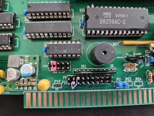
Solder in all the required IC sockets, resistors, resistor arrays, capacitors, jumpers, and the Pololu 5V and 3.3V voltage regulators.  Also do not add 
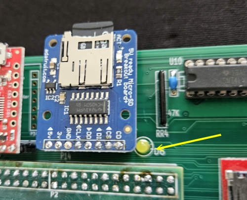
the MicroSD Card Adaptor yet. Please be sure you put the resistor arrays in with the correct orientation of pin 1. An incorrect orientation is one of the most difficult things to detect/debug on a board if not noticed. Check their values before soldering (they are difficult to remove).  Insert all jumper arrays.  
  
The holes for the PS/2 keyboard socket are slightly off -- at least for the Jameco one.  The lowest two pins need to be bent slightly.  Clip off the 3 outer shell ground tags. You can just add solder to the outer shell and the board shell holes when the PS2 pins are soldered in.

Note there are two sockets for the Pololu 5V regulators. While the older ones (D24V25F5) are still available and use P1, it seems Pololu is suggesting users use the newer D24V22F5's (5V, 2.5 Amp) units, it has a different pinout, use this one in P67.  More recently they also added the equivalent D24V22F3 3.3V regulators. Use socket pins P24.  If you use the older Pololu D24V
25F3 3.3 V regulator use socket P4.  Note, you can also use the (less expensive)  EzSBC regulators in P67 and P24 (the rightmost 3 pins in each case).

When adding the LED's be sure to orient them correctly. (Usually the longer lead in the square pad). Add them now.

Please take care to not "slobber" solder on the sockets. They are very closely spaced on this board with vias often close to a socket pin - particularly for the FPGA adaptor sockets. Be sure you also orientate the Keystone 500 (or equivelent) coin battery socket correctly. The + side of the buzzed in toward the right side of the board. Do not add the actual
CR1225 battery yet.  The six PS2 Keyboard socket pins need to be slightly bent to fit as I said above.  You can clip off the outer shield ground pads, just add a drop of solder on the case sides when the pins are soldered in.
  
For prototype boards I generally use "double swipe" IC sockets. For a critical board like this I prefer to use "Machine Tooled" IC sockets.  However they are more expensive and you have to be particularly careful not to bend the IC pins.  Don't forget to add the small 32.768 KHz crystal
X1 next to the RTC socket.

For the buzzer be sure the "+" is on the LHS when viewing the board.
   
For testing you may want to remove every S100 bus board in your system except your master Z80 CPU board, and its RAM board. If you have one, keep the S100 Bus SMB and/or the Bus Display Board). 

As we shall see below during the software build, there are two options for the 80486 monitor console IO. If you have a Propeller Console IO Board, great, use it. If not, you will need to use the onboard USB port connected to a TTY terminal on your PC for monitor IO.  The former option is much better and far easier to get going. It will be a few steps down before you have a working USB port. Except for looking with a logic probe at critical signals you will be in a sense flying blind in that case.  Alternatively you can modify the FPGA (and later 80486 monitor) code to address your own Console IO ports.

Lets get started. Place the board as shown above in the bus without any chips  inserted, (including the Waveshare FPGA adaptor). There are two separate voltage rails on this board 5V and 3.3V. Carefully examine the schematic and check the voltage to the individual sockets are either 5V or 3.3V.  Be sure you have 5V going to the appropriate pins on the Waveshare FPGA adaptor socket.   5V on P7 pin 2, or P8 pin 1 will destroy the unit.

Here is a picture of the board at this stage.
  
   FPGA 486 before chips


Carefully insert the WaveShare Cyclone IV adaptor in its sockets.  No other chips.  Power on the  computer.  "Virgin" Cyclone IV Adaptor boards from WaveShare seem to have the FPGA preloaded with a program (in the EPCS16 Flash RAM) that already that pulses its 4 onboard LEDs.  Note the flashing rate.

Launch Quartus Prime. All the Quartus files we will use are supplied at the bottom of this page.  Typically you would make a folder:

C:\intelFPGA_lite\quartus\18.0\MyFPGAPrograms\FPGA_80486


Within the Quartus FPGA_80486 project folder (the expanded
FPGA_80486.zip download, see bottom of this page).
Place the complete expanded folder at:-

C:\intelFPGA_lite\quartus\18.0\MyFPGAPrograms\
FPGA_80486

Load Quartus and open the Project file 80486_FPGA.qpf, then open the file 80486_FPGA.bdf. When loaded, "
Compile the Design", then "Program the Device" and then hit the "Start" button.  The LED's on the Waveshare adaptor should flash differently - only the FPGA LED L1 should flash. To confirm, kill the power and reboot the computer. The code in the FPGA is lost so the original flashing rates should reappear.   Note,  if you are using a previously programmed FPGA adaptor with code "burnt" into the FPGA the power-on flashing will probably not be present.  In fact,  Waveshare may in the future supply adaptors without the flashing code in them.  
 
Very important the
only the FPGA LED L1 should be flashing.
This is your first connection of the FPGA adaptor to the outside world!  Do not go forward until you see this response.
 
Adding the Board Components
Remove the FPGA adaptor and solder in directly to the board U23 & U25 (74VLC245's) and U2 (a 74VLC373). Re-insert the Waveshare adaptor. 
Also solder in directly U20 (a 74LS240) and U13 (a 74VLC245).  Make sure you have good chips (ideally first tested on another board).
Next add all IC sockets and chips to the board except U5 (the RTC chip), its crystal X1, and the SD card sockets P14 and P15.
Do not install the 32 bit onboard memory sockets P16 and P17 yet.
Carefully install a 3V 80486 chip. Make sure all its pins are straight first before pressing it into its socket carefully. Be sure its pin 1 is the bottom left hand corner. 

Jumper K1 and K3 2-3. Jumper JP1, JP2 and JP3 (the buzzer).
JP12, JP13, JP14 are ground connections for IEEE-696 boards. Not really needed here.
CPU jumper JP4 is normally
closed and K2 open.  Read up on the 80486 to understand the function of those CPU pins.
Jumper K6 and K7 2-3 for now.
Jumper the TMA jumper block, P30 3-4 for the normal Z80 monitor "O" command to transfer the Z80 master bus control to this bus slave.  This assumes you are using a S100Computers Z80 CPU and SMB board.
If not, see the above Prerequisites discussion.
 
The 80486 Monitor Test.
We use a 128K EEPROM in the "ROM" socket U19 with a 80386/80486 monitor program. This is by now a quite complex CPU monitor program capable of running the CPU in real and protected mode, and capable of emulating a PC ROM BIOS to run MSDOS V4.01. It has evolved over the years and is described in detail here. Note the 80486 ROM is not used after power-up on the final board. It's 8 bit bus interface code is moved to the 32 bit wide RAM on power-up (this assumes you have RELOCATE_ROM EQU TRUE in the FPGA_90486.A86 monitor).

Here is the relevant circuit (used only upon boot-up).
   
    
    ROM Circuit
 
You will note the ROM address lines directly interface with the S100 bus. These are drive by the 80486 via
U8, U14 & U11. Also the ROM is always selected, this shortens its access time. Only when 5V_ROM_OE* is low does its data reach the CPU. The 8 bit CPU data bus selection and 5V_ROM_OE* is programed in the FPGA. The S100 bus Phantom* line goes low to make sure no bus RAM data reaches the CPU.  Again remember this whole circuit is only used on power-up. After that the whole ROM circuit is inactivated in the FPGA by a single CPU input of Port 28H.  While not normally used, the ROM can be re-activated by toggling on/off inputs from Port 28H.

The ROM is an 27C010 EEPROM. For now, all code must reside in the upper 64K of tha "ROM" so the monitor starts at 1000H within the ROM.

Recall the 80486 CPU always comes up on power on at
FFFFFFF0H.  We will initially use a simple program loop to write "3's" on the console to test the circuit.  The following code is written into the 27C010 EEPROM at 1FFF0H within the EEPROM. This can be easily done with most ROM programmers. Just be sure it is at the top of the ROM address space (1FFF0H).
 
B0 33     MOV  AL,33H
E6 01     OUT  01H,AL  ;Console IO Board Port
EB FA     JMP  Start


Note this code assumes the Propeller Console IO board at Port 1.
It does not matter what else is in the ROM at this stage. I like to fill it with NOP's (90H). 
Always check your EEPROM you have
B0,33,E6.... at 1FFF0H in your burnt ROM. 
Here is a picture of what should appear on the screen.
       
Output 333
  
This simple test loop must work flawlessly before going any further.
 
As we discovered years back,  the 80486 WR signal comes out too early for most S100 bus boards. It must be delayed with the following FPGA circuit.
   
  Delayed pWR
 
The above settings should work for most S100 bus RAM boards, but if you see RAM write errors try changing the 74164 "jumpers" in the FPGA diagram.  Here is the desired signals using the above pre- and post-pWR- delays:-
  
  80486 SBC Signals 2
  
Observe how the S100 bus pWR- (red) signal is well within the sOUT (brown) and MEMW (brown) signals.

You can check these memory writes in your S100 RAM by hand writing the following bytes into your "27C010" EEPROM at 1FFF0H.
 
TestB:  
31DB     XOR BX,BX
8EDB     MOV DS,BX     ;Set segment 0:0000H
B033     MOV AL,33H
8807     MOV [BX],AL   ;Write to RAM at 0:0000H
8A07     MOV AL,[BX]   ;Read back from RAM
E601     OUT 01H,AL    ;Display the result (must be 3333's)
EB       JMP TestB

Your console should display only 3333's

Alternatively you can assemble the
FPGA486 monitor code (see below), with "TEST2 EQU TRUE" at the start of your FPGA486.A86 code and burn it as a .bin file with your ROM programmer.
  
  TEST 2
   
Again your console should display only 3333's


LOADING THE ROM MONITOR
If both these tests work there is a good chance the critical components of the board are OK. Next we will burn our complete FPGA486.bin file (supplied below) into the EEPROM. 
Since we have no onboard 32 bit RAM yet, we need to set
Dip SW1-1 to ON (See below). This will prevent the monitor ROM being relocated to 32 bit RAM (currently not added) upon reset.
In summary:-

SW-1 on (closed)  - in this position the following happens:

  • The on-board RAM module is disabled
  • The monitor is run directly from ROM
  • The board’s memory space is limited to 64K of S100 RAM. It will not be possible to boot MSDOS, and it will not be possible to access the “Protected Mode” ROM monitor menu


SW1-1 off (open) – in this position the following happens:

  • The on-board RAM module is enabled
  • The monitor software is copied from ROM to the on-board RAM module, and is run from RAM
  • The board’s memory space is 16MB of on-board RAM, with the exception of the bottom 64K provided by the S100 bus
  • This setting is required to boot MSDOS

SW2 on/closed sends Console Output to the VGA board SW3 on/close takes Keyboard input from the boards PS2 port.  SW4 on/closed used the USB port for all Console IO.
These are for teh FPGA ROM monitor commands. MSDOS programs will need BIOS "adjustments".

     
    IOBYYTE Switch
    

Remember the initial boot code has to reside in the ROM so the CPU reads it at address FFFFFFF0H. We use a 128K EEPROM (a Greenliant
GLS29EE010 or similar chip). As mentioned above, this chip can be looked at as two 64K ROM blocks. The monitor code it must reside in the upper 64K block of its final 128K bytes.  Here is what you do for most Wellon programmers:-

To burn say a GLS29EE010 EEPROM's with a Wellon VP290 Programmer...
Load the FPGA486.BIN file. Set "To Buffer Address (HEX)": 10000
Change nothing else. (The Dialog box should be:- Normal, Normal, 0xFF,0, 2000, Binary)

The file is
FPGA486.bin (see the bottom of this page to download it).
Here are pictures of the process using a Wellon Programmer.
      
  Wellon VP290
      
Next load the 80486_FPGA.brd file into Quartus, assemble it, and use it to run the FPGA in the Waveshare module and transfer control to the board with your Z80 CPU board Z80 monitor
"O" command.
Make sure Dip SW1-1 is ON to inactivate the ROM software transfer code to RAM.
 

The 80486 should sigh-on as shown here:-
       
    Monitor Signon
    
Note with SW1-1 on there will be no ROM relocation to RAM.

The "
K" command shows you the menu options in 80486 real mode.

Since we have not yet added the onboard 32 bit RAM the monitor/FPGA as configured in default mode only has the lowest 64K of S100 bus RAM active. This can be easily changed in the FPGA .brd file. However since the 80486 is not addressing this S100 bus RAM in 32 bit mode normally we will keep the S100 bus RAM "window" to a minimum -- if indeed you need it at all.  Here is the FPGA 80486.brd relevant section for the RAM addressing.  Please study it in Quartus.
    
  FPGA RAM ADDERSSING
   
To recap, after a reset the 80486 boots to 0FFFFFFF0H in the onboard ROM, address by the ROM S100_ROM_SEL-. It will do a far jump to 0FF000H also address by the ROM S100_ROM_SEL-.  As described above,  any CPU address less than 64K will activate S100_RAM_ACCESS-. Any CPU address above this range will activate 32_BIT_RAM ACCESS-, in particular RAM_CS- to the onboard 32 bit wide RAM. There is however a carve out window in the first 1MB for VGA RAM and a VGA ROM if a VGA board is present (See S100_WINDOW).

The 80486 has a complicated process to address 8, 16 and 32 bit memories at any address position.  It can be forced to do only 8 or 16 bit modes by its two pins
BS8* and BS16*. Much of the complexity at the bottom of the Quartus FPGA486.brd file is devoted to the required logic to handle this process. The net result to the user is the 80486 interfaces the S100 bus as 8 bits with a 10MHz clock  and the 16MB onboard RAM as 32 bits with a clock speed increased to 16MHz - 30MHz.


Adding 16MB of 32 bit wide Onboard RAM.
Next we will add the 16MB of 32 bit wide onboard RAM. There are many ways to add onboard RAM to this board. In fact we could even add a little 32 bit wide RAM programmed into the FPGA module itself.  Best would be a DRAM SIMM module. However I'm currently not capable of doing a circuit to refresh these chips. I ended up with four 4MX8 Alliance AS6C3216 Static RAM chips.  The advantage of using 4 separate chips is the DWord, Word and Byte memory access issue is easy to do in hardware.  Each chip has its own CS* line for each byte within the 32 bit address.

Here is a picture of the 16MB RAM module. You will need to carefully solder these SMD to the RAM  mini-board.
   
  16 MB RAM Adaptor
 
See here for a description of the soldering process. 
These are expensive chips (Digikey # 1450-1414-ND, ~$6 each). Note these are completely differen mezzanine RAM boards from those we use on our 16MB S100 bus RAM boards (which were only 16 bits wide).  It is absolutely essential you test the integrity of the above RAM. The FPGA486 monitor has some extensive test to do this. You need to boot the board with the RAM module in place with the Z80 monitor "O" command. This brings up the 80486 in Real mode. To access RAM above 1MB you need to run the 804 86 in Protected mode. Pressing the 80486 menu option "O" will switch the CPU into this powerful addressing mode. From here you can run various tests on all 16MBs of RAM with the "J" command. Note these detailed tests cover a huge expanse of RAM. Even at 30MHz they take well over 1 hour to run completely.

Here is a Memory map of the first 1MB of RAM in 80486 Real Mode.
  
     MM with VGA
Note this is for a system which contains our Cirrus VGA board. If that board is not present everything will be RAM.

At this point you can also put the CPU into its "Protected mode" which allows the full 16MB of RAM addressing. To do this, from the Z80 use the "
O'" command., and then a second "O" command.

Here is an example of a run.

      
    RAM Test
  
If you pick up a string of errors, chances are you have a RAM pin soldering problem.  Layer some solder flux on all the RAM pins and briefly run a hot solder tip along the pins. Spray off the excess flux and check for cross bridges.

All tests must run without errors.  If you get to this point you are well on your way to having a very functional board.

Note the CPU is driven at two clock speeds. 8MHz for S100 RAM and IO and at 16Mhz for the 32 Bit RAM.  The signal "
32 bit_RAM_access"  flags which clock speed is needed.
For clock speed switching one has to be carefull "Runt" clock pulses are not generated during the switching process.  I nice circuit is illustrated here that prevents this.
  
    Dual Clock Speeds


Adding the USB Serial Port
We will now add a USB Port for an alternative Console I/O to the board. 
This will be a relief to those that do not have the Propeller Console IO Board and may have been flying almost blind up to now. 
There are numerous Serial to USB converters available these days.  This board will work with these common Adfruit or SparkFun ones shown here:-
   
   USB Adaptors
   
All 3 fit into the socket P33. I actually prefer the FT231x, but the Adafruit CP2104 brings out RTS and CTS to the bottom P3. This is useful for fast connections (XModem etc.).
Note the USB side sockets P32 & P34 are unused, they are only there to stabilize the adaptors and in fact need are not needed.
Also is the first time we will be using Public Domain software modules. These are available for chips like the Cyclone IV Series in many places on the web.
I mention in particular OpenCoresJavier Valcare's FPGA home page and fpga4fun.   In most case however the source is in VHDL or Verilog "raw" format.   Fortunately Quartus allows you to convert the module to a .bsf file so it can be used directly in our (growing) FPGA486.bdf file.

In this case we use the UART.V file from OpenCores Then under the File menu:- Create\Update, Create a Symbol File from current file. We create uart.bsf. Then within the Quartus Symbol Tool, under Project, you will find uart. Drag that into your growing .bdf file --  I always add components at the bottom of the growing
.brd file.
This is how one adds software modules in Quartus.  Its already loaded for you however in our version of FPGA486.bdf.
Here is the core circuit within that file.
        
 USB Circuit
   
The above circuit is actually an RS232 UART circuit.   We use one of the above RS232->USB adaptors to convert the bidirectional data to a USB format.  As I said above, I like to use the SparkFun FT231x.  It's simple and reliable and uses a USB micro connection. It can run at 5V or 3.3V. Since we are connecting the chip to the FPGA directly you need to jumper the chip on the back to 3.3V. SparkFun also supplies a SparkFun FTDI "Basic" converter, FT01, which uses the older USB mini connector -- same pin connections.

On the receiving side you will need a PC TTY terminal. Again there are many.
I like the Telnet Program Absolute Telnet. Select "Properties", then select "Connection". Your SparkFun windows driver should appear as a COMx port. If you pull out the USB cord that COM port should disappear from the "port" dropdown menu.  It will reappear if you reconnect.  Set to 38400 baud, 1 Stop bit, No parity.  Another good Telnet program is Tera Term. This one can be downloaded for free from here.  The default data USB data port is at 82H.  So from the FPGA486 monitor if you enter:-

QO82,33

You should see a "3" on the USB/TTY terminal.  You must see this to continue.

Console IO Switches
On this board there are 4 different I/O possibilities for a Console I/O for the 80486 Monitor (and MSDOS).
1.  The Propeller Console IO board.
2.  A USB port connected to a PC and a TTY character terminal.
3.  For both of the above,  the keyboard can instead come from a PS2 keyboard connected to the boards PS2 socket P35 (or P18)
4.  For all 3 of the above,  the Console output can instead go to our S100 bus VGA display.
We will discuss the PS2 Keyboard and VGA connection further below.

The decision in the FPGA486 monitor is based on the lower 3 bits of the 8 bit FPGA_IOBYTE port (
8EH). Defined as follows:-

CONSOL IN/OUT:-
; FPGA_IOBYTE xxxxx111B
Propeller IN and OUT
; FPGA_IOBYTE xxxxxxx0B
USB Port IN and OUT
; FPGA_IOBYTE xxxxxx0xB
PS2 keyboard IN, Propeller or USB out (depending on bit 0)
; FPGA_IOBYTE xxxxx0xxB
Propeller, USB or PS2 keyboard IN, always VGA Video Board OUT in MSDOS

Upon initialization the ROM software reads the lower nibble of the
FPGA_IOBYTE (port 8EH, set with SW1) and copies it to the upper nibble of FPGA_IOBYTE port 8EH. Later in software, these upper 4 bits can be changed if desired allowing for dynamic console I/O redirection. Remember however with a hardware reset the SW1 bits are always reapplied to the FPGA_IOBYTE upper nibble.  Here is an example where we use th USB port for Console IO (xxxxxxx0B).
           
 
  USB Port as console
  
With all 4 switches open, the FPGA80486 monitor always boots up with the Propeller Console IO board for keyboard input and video output.
Note the VGA board will only be activated in MSDOS. In the monitor mose DIP SW2 has no effect.

Please note that when you bring up MSDOS with this board/monitor there is an additional option to have the
MSDOS Int 10H driven console output directed to either the Propeller Board, the USB port, the VGA video board or the S100 Computers Lava Video board.
The main menu "B" command allows you to select this option before booting up MSDOS. Remember this is only for MSDOS
Interrupt 10 driven console IO.
        
  MSDOS IO Configuration


Adding the PS2 Keyboard Interface.
As an alternate for the FPGA486 Monitor CONSOL input we will add the PS2 Keyboard for input as mentioned above. 
 
The PS2 module have been described and used with our V2 FPGA board
    
     
      PS2 keyboard
    
Note the PS2 can also be connected to ribbon cable (via P18) that can be connected to the back of your S100 Box. The pin-out is the same as for all our earlier boards. Here is the Signon image you should get upon reset:-
   
   VGA Display
         
Remember however that the above redirection of Console output is based on the
FPGA_IOBYTE within the 80486 Monitor (SW1).
If you load MSDOS or other software that use the standard MSDOS/IBM PC BIOS interrupts/calls (
INT 10H) they will utilize the console output requested by the monitor "B" command as mentioned above. 


The RTC Circuit
Next will add the Clock/Calendar Maxim DS1305 chip U5 to the board.  Also add a CR1220 or CR1225 3V "coin battery between jumpers
P38 & P39. 
Make sure the "+"  terminal of the Keystone 500 holder is on the RHS.
Unlike all previous boards, this one is designed to use a Keystone 104 battery holder which requires use of a smaller 2320 or 2325 coin battery and less board space.
This is a simple, but an extremely powerful, 16 pin DIP  chip.  We previously used it in our FPGA Z80 SBC board.
It will handle almost any date/time requirement you have.  It is described in detail here
As you can see the interface can be via a SPI or I2C connection.  I have chosen an SPI interface (Pin 9 of the DS1305 to Vcc33). 
The trick was integration the interface into the MSDOS compatible ROM BIOS to get accurate date and time stamping on files etc.
The FPGA SPI/RTC module is already in our FPGA486.bdf file.  Our ROM BIOS has the appropriate code to read the RTC on MSDOS bootup and put in the correct Time and Date for file stamping.

MSDOS on the original PC utilized a 18.19Hz interrupt to increment a counter in RAM to track the time changes since bootup.   That simple and rapid counter tracks if the operating system crossed a midnight boundary.  When that happens the current date must be updated.  MSDOS gets the actual date/time for file stamping by looking at the timer pulse number and back calculating.

Currently I have not succeeded in programming the DS1305 chip to produce an interrupt pulse (
RCT_INT*) counter which it is capable of (see SET_RTC_1SEC_INT in the ROM BIOS). To emulate this currently I'm just using the ~1 second interrupt comes in on the S100 bus VI2 line from the SMB V4 board.   In case some MSDOS software requires such an interrupt Jumper P10-2 to P9-2.  Keep in mind this interrupt is not needed for file data an time stamping. MSDOS reads the RTC directly in the ROM BIOS.

When you first boot up the system you must initialize and set the data and time with the FPGA486 monitor "E" command. 
You can also do it within MSDOS with the date and time command prompts.  Here is an example setup:-
   
   Set Time
  
Now when you load MSDOS the time will be correct.
  
      MSDOS Time

I should point out that over time the displayed time can be a few minutes off in 24 hours. I have not debugged this yet.

 
Adding The SD Card Interface.
This is perhaps the most complex aspect of this board.  Not only in terms of the software but because today SD cards come in all shapes and sizes.  There are numerous articles on the web describing how to determine the type of SD card present and even more articles describing how to "initialize" them.  Three good articles that help me a lot are:
Secure Digital (SD) Card Spec and Info
What is the correct command sequence for microSD card initialization in SPI?
and the excellent code example by CC Dharmani, see here

The interface is a complete transplant from the FPGA Z80 SBC board and FPGA_80286_SBC board.  The code below will read and write to today's very common Type 2 SD cards.  It would have to be modified to work with the older Type 1 cards.  These require a different initialization sequence.  Experienced SD programmers may note during the card initialization sequence I add valid CRC bytes to the initialization commands before turning off CRC checking.  I also actually set the sector size to 512 bytes .  Many programs do not do this but the are reports of some Type 2 SD cards actually requiring these steps.

As to the actual Type 2 cards themselves, they come in two sizes of "Micro" adaptors. 
This board can use one Adfruit Micro SD adaptor (
P14) and one SparkFun Micro SD adaptor (P15). In other words you can have two SD card drives A & B. 
There is a slight error on the board. The pullup resistor for the Drive A "SD Card Absent" LED is 47K. It needs to be 330.  Please jumper a resistor as shown below
SD Card Adaptor   SD card LED   SD Card Resistor

Because we are interfacing the SD card with our 3.3v FPGA we can essentially connect the SD card directly to the FPGA. This is what these adaptors do.  The Adfruit adaptor runs with the 3.3V supply pin input.
Using an FPGA really illustrates the utility of these FPGA chips.  We use our now tried and true SPI interface to talk to the SD cards.  Here is the core SD card SPI interface module.
       
  SD_Module 
   
It's the same as the one we used for our FPGA Z80 SBC. We will allow for two slave/SD drives. These are selected outside the above module by outputting a bit to the CS*  pin of the SD card (SD_CS_STATUS-)

You will note that we use two SPI clock frequencies.  This is because during a cold start, SD cards only communicate over the SPI lines at a slow (~100-200KHz). Once Initialized, this can be jacked up. I use 10 MHz here.  The 21mux controls this by a high/low bit from the SPEED_PORT.
We will require four I/O ports:-

SD_CARD_BASE EQU 078H

SD_DATA_OUT     EQU    SD_CARD_BASE     ; (78H) Data to SD CONTROLLER
SD_DATA_IN      EQU    SD_CARD_BASE     ; (78H) Data from SD CONTROLLER
SPEED_PORT      EQU    SD_CARD_BASE+2   ; (7AH) HIGH TO READ/WRITE SECTORS WITH HIGH SPEED SPI CLOCK
SD_CS_PORT      EQU    SD_CARD_BASE+4   ; (7CH) SD Card CS* Select Port
SD_STATUS       EQU    SD_CARD_BASE+2   ; (7CH) SD CARD Status Port
SD_RW           EQU    SD_CARD_BASE+3   ; (7EH) Port to pulse SPI Read/Write interface


Initialization of Type 2 SD Cards.
You can skip this section if you like since what is here is already in the Z80 SD_CARD software describe here.

In order to use an SD card you must first "initialize" it.  This requires a series of 48 bit SPI commands.  These must be sent in the correct sequence, not continuing forward until the correct response from the previous command is obtained.  Sometimes this involves repeated sending of a command. 

The commands themselves all have the following structure.
       
  SD_card SPI Format 
  
The first byte contains the actual "Command". All SD card commands have the following format 01XXXXXXB.
Here is a list of the commands we use:-

CMD_0:   DB 40H,00H,00H,00H,00H,95H,0FFH ;   (0+64)  CMD0   To Reset the SD Card interface,
CMD_1:   DB 41H,00H,00H,00H,00H,0F9H,0FFH ;  (1+64)  CMD1   Activate Init Process
CMD_8:   DB 48H,00H,00H,01H,0AAH,87H,0FFH ;  (8+64)  CMD8   To check Card Voltage
CMD_9:   DB 49H,00H,00H,00H,00H,8FH,0FFH ;   (9+64)  CMF9   Read SD Register (CSD)
CMD_13:  DB 4DH,00H,00H,00H,00H,081H,0FFH ;  (13+64) CMD13  Get SD card status
CMD_16:  DB 50H,00H,00H,02H,00H,081H,0FFH ;  (16+64) CMD16  Set Sector size to 512 Bytes
CMD_17:  DB 51H,00H,00H,00H,00H,0FFH,0FFH ; (17+64) CMD17  Read a single block (Block 0, Used to load boot sector only)
CMD_41:  DB 69H,40H,00H,00H,00H,077H,0FFH ;  (41+64) CMD41  Activates the card's init. process.
CMD_55:  DB 77H,00H,00H,00H,00H,065H,0FFH ;  (55+64) CMD55  Application specific command NEXT
CMD_58:  DB 7AH,00H,00H,00H,00H,0FDH,0FFH ;  (58+64) CMD58  Read SD Cards OCR register
CMD_59:  DB 7BH,00H,00H,00H,00H,0FDH,0FFH ;  (59+64) CMD59  Turn off CRC checking


You will note there is always a "stuffer" byte 0FFH byte sent before a return response byte(s)  from the SD Card.  The return Flag byte contains the error code if any.  Generally (but not always),  you want to receive 00H.

The sequence to initialize Type 2 SD cards is as follows.

Drive the CS* pin from high to low
Send 24 or more dummy 0FFH bytes.
Then send the following 6-byte command,  First byte: 0x40 (CMD0), Next four bytes: 00000000H, then the CRC byte (95H), then send another dummy byte 0FFH byte.
Read the returned byte from the SD Card.  If its not 01H,  repeat this command until 01H is returned.
This means the card is in the "idle state" and we are good to go.

Next send the following 6-byte command,  First byte: 0x48 (CMD8), Next four bytes: 000001AAH, then the CRC byte (87H), then send another dummy byte 0FFH byte.
Read the returned byte from the SD Card.  If it is 01H you probably have a Type 1 SD card. We want a 05H returned, indicating a Type 2 card.
We confirm this by reading the next 4 bytes from the SD card.  If its 000001AAH, we have a Type 2 card for sure.

Next we "activate" the Type 2 card by sending two back to back commands CMD55 and CMD41 exactly as done above for the CMD0 command.
Repeat the latter two commands continuously until you get a return 0H byte.

The SD card specifications says that only CMD0 and CMD8 should have a valid CRC byte in SPI mode, however there are reports that some SD cards (like Transcend ones) seem to require a proper CRC for CMD55/CMD41 commands as well. To be on the safe side I add the byte.
Also between every command above,  the SD card CS* line needs to be lowered and raised when done.

Based on other web postings, I also send CMD59 to specifically turn off CRC checking and CMD16 to set the sector size to 512 bytes/sector. 
I'm not convinced these are essential but it's best to play safe.
Here is an example picture of the main SPI signals using the CMD8 command:
   
  SD Card Signals 
       
I have written a small 80486 module to initialize, read and write sectors to the A,B and C SD drives in the ROOM BIOS. The program allows you to test the SD Cards interface.
Here is a picture of the main menu:-
   
  SD Card Menu
  
Please note this is not a "bullet proof" menu. Little command error checking etc. is done.  The sector numbering is only 0-FFFFH, but that should be enough for most needs.  In fact some older Type 2 cards may not accept a sector number this large. 

Note. These SD cards can read and write multiple sectors with a single SPI command. I have not added this feature yet.
Also keep in mind  the SD cards LED D6 will only light up if a SD card is not inserted in the Adfruit Micro SD adaptor (
P18).  It is not connected to P17.
 
Please examine the 80286_FPGA.bdf file to further understand the SD card interface on this board. 
Also spend some time studying the 80486 monitor code. 
All the critical routines:  Initialize, Read Sector, Write Sector etc. are written as self-contained returnable calls which should make it easier to incorporate them as a MSDOS BIOS etc.
The source is in .A86 format for use with NASM.

This program is transplanted almost unchanged into our  FPGA-80286  ROM monitor and is brought up with the 'H' command in the main menu:-
    
You therefore can have 2 different SD card drives running on this board. 
You can change the monitor drive equates and the FPGA.bdf module to switch them around (bits 0 and 1 of the SDC_SC_STATUS port).

You can also of course boot MSDOS (Monitor 'P' Command ) from your S100 bus .
Currently I have not modified the FPGA ROM monitor to load MSDOS from the SD cards (for the IDE/CF card board it is already done).  Volunteers needed -- everything in hardware is there!

One final note, a useful PC program to see/check what is written on any sector of an SD Card is HxD Hex Editor.
It can be downloaded from here.


Interrupts.

U15, the 8259A Interrupt controller we will use the Propeller Console IO Board key press interrupt for testing.  It comes across on the S100 bus pin 6 (VI2).
This interupt is fed to the 8259A by jumpering P9-3 to P10-2.  See the picture below.
To test the interrupt circuit bring up the Monitor
L menu.  Any character you type will issue an interrupt and be picked up by the board circuit and displayed.
This function must work correctly to run MSDOS on this system.
  
   Keyboard Interrupt Jumper   Interrupt Test

   
MSDOS
You now have a complete functioning 80486 CPU board.  You should be able to run MSDOS V4.01 "right out of the box" -- just like our other '86 boards. 
Currently software to boot MSDOS from either of its on-board SD cards is not written.  Perhaps somebody could add this.
You need to use the IDE/CF card board.  The MSDOS card must be in drive B: (A: is always for CPM3).  MSDOS can be downloaded from here

Note the MSDOS support board should not be in your system with this board. It's functions are supplied by the FPGA.
  
   MSDOS Signon


Burning FPGA Code to Flash RAM

Up until now whenever we programmed our FPGA via  the JTAG socket the data is lost whenever the power is turned off.   While fine for code development etc. it is not desirable for a final board configuration.  Like most FPGA applications the "final" code is saved in Flash RAM and immediately loaded by the FPGA each time upon power-up.  This is a standard and common characteristic of most FPGA's. Some older models in fact had a ROM onboard.    Our Cyclone IV Adaptor board has 16MB of Flash RAM on board for this purpose -- way more than we are ever going to need!

The tricky part is programming this Flash RAM.  I found the Intel documentation poor and confusing.  Here is a summary of the process: 
  
Within Quartus you need to "convert" your normal JTAG FPGA .sof programming file to a special file .jic to program the Serial Flash RAM chip on the Weveshare board.

Within Quartus, click on the File Menu and select "Convert Programming files". The dialog box below will popup.
From the dropdown box on the "Programming File Type"  select a .jic file type.
This is the file format that is required to program the onboard serial Flash RAM.
For the Options/Boot info select EPCS16. Leave Active Serial as is.
You can name the .jic output file anything you like. I usually just leave it output_file.jic.
Note it will be in the Quartus generated "output_files" folder within your work directory.

Next click on Flash loader within the lower "Input Files to Convert", then click on the highlighted "Add Device" button.
You will get a popup dialog box as shown below.
Select Cyclone IV  and EP4CE10.  Note Quartus takes some time to allow you to actually select these options -- seems to be doing things in the background!
Next click on "SOF Data" and "Add File".  You should see your "normal" FPGA program .sof file in your "output_files" folder within your work directory.
Finally click the "Generate" button.
You should get a popup dialog saying "Generated output_file.jic successfully.
Note the name and location of the converted file. Then close that dialog box.  See the pictures below.
   
   Programming 1   Programming 2
       
  Programming 3   programming 4
       
  Programming 5   programming 8
                           
Next we need to actually flash the Waveshare boards RAM chip.
Click on the normal "Program Device (Open Programmer)" you normally use. If its not already open,  give it time to come up as a dialog box.
Make sure your board has power.  To be safe click the Auto Detect button. your normal xxx.sof file should display with the device set as EP4CE10F17.

First delete the above line xxx.sof  |  EP4CE10F17 etc.
Click on Add File and select the xxx.jic file you just generated above.
Click on the Program/Configure little square character boxes.
The chip diagram below should show only 2 chips as shown. If more right click on any 'extra' one and delete it. The dialog box must look as shown below.
The Start button should highlight.
Click on this and you will flash the RAM chip.  Follow the Progress bar until it is done -- it takes about 1 minute.
You can power off and re-power your computer.
Your FPGA board should (after reset), start with whatever FPGA code is within the chip.

To recap, in the \output_files  will be (amongst other things):-
80486_FPGA.sof   This is the "normal" build file during testing etc. The FPGA looses this data upopn power-down.
FPGA_486.jic       This is the file you use (made as described above)  to program the FPGA permanently. It will work after a power-down.
Both files are seperately listed below.

Note when you close the above dialog box, normally you do NOT save the changes.
Typically you want the chip to be quickly reprogrammable.

Jumpers
The board has a few jumpers that may not be obvious.
K6 and K7These jumpers are normally 2-3.  If you want the board to be an S100 bus master they would be 1-2. However the Quartus.brd file will need to be modified as well.
                    The position 1 of K6 and K7 by default are connected to the FPGA Delay_1 and Delay_2  signals within the FPGA code to manage the pWR* signal delay (see above).
                    Pin1 in each case it there to attach a logic analyzer.
JP1               Some S100 bus systems provide the 2mHz clock signal (Pin49) from the front panel.
JP2               Some S100 bus systems generate the MWRT signal (pin 68) from the front panel. If your board does this then don't jumper JP2.
JP4               Pin R17 on a 80486 CPU is used to control the internal core speed of the DX4 processor. The CLKMUL (Clock Multiplier) signal at pin R-17 is sampled only during a reset
                     of the CPU and defines the ratio of the internal clock to the external bus frequency CLK signal at pin C-3. We will jumper JP4
K2                 Pin A15 on a 80486 (IGNNE) when grounded causes the CPU to ignore floating-point errors. Jumper it 1-2.
K1 and K3    These jumpers are normally set 2-3.  For a S100 bus master configuration of the board they should be 1-2. However the FPGA code also needs to be modified.
P3                This is a spare pin from the Waveshare FPGA to allow you to examine any internal signal.
K4                 Normally this pin is 2-3. Its there because P7-53 is not connected on Jeff Wilsons T35 FPGA board.
K5                 Normally not jumpered, (the TMA0 (P30 3-4) line switches the slave in).  
                     Jumpered 2-3 forces the board to power on as an active slave, P30 1-2 must be jumpered as well.
                     K5 jumered 1-2 (along with P30 1-2) immeciatly forces the CPU to active slave mode when the jumper is grounded.


The following board jumpers can be used to analyze some critical signals with a logic analyzer:-
P2           
     Delay 1 signal for pWR*
P11               Delay 2 signal for pWR*
P12               FPGA_pWR*
P19               FPGA_pDBIN
P20               CPU_CLK
P23               FPGA_sMEMR
P25               FPGA_MWRT
P21               FPGA_sINP
P22               FPGA_sOUT
P26               CPU_MIO*
P27               CPU_WR*
P28               CPU_DC*

The LED's on this board indicate:-
Waveshare L1  The FPGA is active and functioning if flashing.
Waveshare L2  Output to port 2CH forces a board reset and flashes this LED.
Waveshare L3  Indicates a 32 bit RAM access  is underway.
Waveshare L4  Output to port 28H inactivates the board RAOM and activates this LED
Board LED D1  Flashes whenever the S100 bus RAM is accessed
Board LED D2  Flashes whenever the CPU issues a sINTA signal to teh S100 bus
Board LED D3  Flashes whenever the 80486 has control of the S100 bus.


Notes

No hardware changes have been noted to date. The pictures of the board on this page is actually that of the final prototype board. The actual "production" board has some very minor changes -- mostly silk screen text changes. However. Over time there may be corrections/additions to the 80486 monitor or FPGA .bdf files. Always check below and use the most recent versions.

I have tried to substitute a mazzine RAM board containing 32 pin DIP RAM chips (AS6C4008's) but I could not get the FPGA code correct to use them.
If somebody wishes to try this board I can send them one.  Here is the relevent schematic.

Speed, I have had the 32 bit RAM running at 30MHz but it's not 100% reliable - fails on an overnight test.
Reducing the speed to 16MHz corrects he problem.  However I believe the CPU is capable of running at higher speeds if one had time to play around with the CPU Rd/Wr and Wait signals in the FPGA code.
I have not had time to examine this.  The P2 to P28 pins are there for a logic analyzer.  If you do better please let me know.

Please Note. I recently discovered that you must have the 64K S100 bus RAM in lower memory to load MSDOS. Using 100% 32 bit onboard RAM does not work. Probably something to do with interrupts! 

Parts

It is critical you use a 3V 80486 CPU.  These chips run at 3.3V (+/- 0.3V).  Intel chips  which require 5V and will not run correctly on this board.

Fortunately these chips are fairly common on ebay however there are a number of different AMD-DX4 chips. Please try and get the exact AMD-DX4-120 one shown below.

I have tried a few other AMD chips with different speeds and voltages. It's not clear to me why they did not boot. I suspect some of the FPGA timing/wait state signals need to be modified.


    80486 COU
 
Also at the clock speeds we are using here (16 mHz) there is no need for a CPU heat sink.  The chip does not even get very warm.

There appears to be a few variations of the
74LVC245 20 pin DIP level Shifters chips with "A", "AN" etc. after the 245.   As best I can tell so long as they are 20 pin DIPs they are all OK. I use Mouser chips # 595-SN74LVC245AN.  

The WaveShare Cyclone IV adaptor can be obtained directly from Waveshare
You also might want to get the USB Blaster/Programmer from them.

The WaveShare unit uses unusual 2mm dual row pin connectors. See the write-up above. The best sockets are the Digi-Key #1212-1786-ND 100 pin sockets (carefully clipped to size).

The USB serial Adaptor is from Sparkfun F1231x.  The Micro SD Card adaptors are from Adafruit  and
Sparkfun
 
Please note the sockets for the WaveShare adaptor are quite tricky to fit on to the board.  I found the best way to do it is (after trimming to size), push them half way on to the adaptor pins and then wiggle them to fit the whole unit on to the S100 board.  Figure on spending 10 minutes on this step!  Do not solder them to the board first and then try and press the adaptor down on them. They are very fragile and internally the leaves will bend if socket angles are not exactly correct.  When in place, check each pin is visible on the back of the board before soldering.  Only then solder all around.  Add as little solder to each pin as possible - the narrow pins have a tendency to wick up solder internally. 

To remove the adaptor,  leaver each corner up a little going round and round. The first time its quite difficult to get the adaptor out. It gets easier with time.

AS6C3216 and AS6C6416 chips.
In an earlire writeup of this page I suggested using
4X16MB ASC6416 RAM chips.  This was an error, you can use the cheaper  2MX16MB ASC3216 chips.
If you have already slodered in your chips you can stabalize the floating RAM
pin 13 on the ASC6416 chip by a solder bridge to its pin 12.
Here is a picture:-
   
    RAM correction


Installing Quartus Lite on Windows.
In spite of its name the
Quartus Lite IDE is a large program.  When fully installed the Quartus folder is over 15GB in size.  Installing it makes Microsoft's Visual Studio seem lightening fast! 
 
That said,  its an excellent IDE.  Figure on 1 hour to install and get it right.  For our purposes we will only be using probably 5% of its capabilities, but I have found if you try and get smart by not downloading or removing sections you run into problems later during usage. 

Please see here for instructions on how to install Quartus. 
 
Note to add slaves to the system with the FPGA_80486 SBC you will have to modify the FPGA486.bdf file further.

Its very important not to get the Quartus/FPGA files mixed up with those for those described above.
They should all reside in a directory such as:-
   
C:\intelFPGA_lite\18.0\quartus\MyFPGAPrograms\80486_FPGA


You have to be very careful with file associations Quartus uses during compiling. If strange things happen close the program completely and start again.
 
A Production S-100 Board
Realizing that a number of people might want to utilize a board like this together with a "group purchases" by people on the  Google Groups S100Computers Forum was opened. It is now closed.

At a later date a second batch of boards may be done by Todd at:- https://www.retrobrewcomputers.org/doku.php?id=board inventory

Please see here for more information about this and other past S100 Boards.  Please do not contact me directly. 

FPGA 80486 SBC (V2.1A) FINAL Folder.zip        This .zip file KiCAD components required to build this S100 board   (V2.1A  4/9/2024)
FPGA 80486 SBC (V2.1A)  Gerber.zip                Gerber files to manufacture the board with JLCPCB  (V2.1  12/28/2023)
FPGA_80486_SBC (V2.1A) Schematic PDF file    Board Schematic (4/9/2024)  

32 Bit Mezzanine RAM Board.zip                      
 (12/14/2023)
32 bit Mezzanine Board Schematic (PDF)           
(12/14/2023)
32 Bit Mezzanine Board Gerber.zip                   
 (12/14/2023)

Main Quartus 80486 SBC Folder .zip                 This .zip file contains the FPGA_Z80 build   (02/23/2024)
FPGA_80486_Monitor.zip                                This .zip file contains the 80486 monitor BIOS source and .BIN files       (V2.33   1/30/2024)  
FPGA Monitor Source Code                             
This file contains the source code of the FPGA 80486 Monitor  (V2.33   1/30/2024)  

80486_FPGA.sof                                            
File to program the FPGA. (Lost upon power-down)   (3/17/2024)
FPGA_486.jic                                                 
File to to program the FPGA permanently.                (3/17/2024)

Quartus-lite-21.1.1.850-windows.tar                 
This is a .tar file containing Quartus Lite and support programs. Note it's almost 6GB in size    ( V1.31   6/9/2020) 
Quartus-lite-21.1.1.850-windows.zip                 
This is a .zip file containing Quartus Lite and support programs. Note it's almost 6GB in size    ( V1.31   6/9/2020) 
FPGA_80486 SBC BOM (text file)                        

FPGA_BOOT.AVI                                           
Here is a video of the FPGA_80486 booting MSDOS from our IDE/CF Card board.

Other pages describing my S-100 hardware and software.
Please click here to continue...

This page was last modified on 05/01/2024