S100 Computers

HomeS-100 Boards HistoryNew BoardsSoftwareBoards For Sale
ForumOther Web SitesNewsIndex   
  
Parallel Ports IO Board
  
  Production Run-2
 
Introduction
The simple parallel port is an often overlooked component of an S-100 system.  Apart from driving printers and other hardware devices,  a straightforward parallel port with no need to initialize it beforehand etc. is very useful for debugging a system.  A simple monitor command to output a byte to a parallel port (or input one) can often very quickly identify a problem.  If a board with such a port had an LED bar to indicate the status of the ports bits then things really get convenient.

Using as a starting point the original IMSAI PIO board we will elaborate a bit on that old but very reliable board.   The board utilizes the Intel 8212 parallel port IC chips.  While these originated in the mid 1970's and are large,  they are extremely well suited to having a simple parallel port without software initialization etc.  They have one other advantage over the smaller and simpler 74LS374 style chips in that they provide a strobe signal for outputs and can provide an interrupt signal for inputs.  Very useful is the fact that the external strobe signal can latch the input data and hold it until the CPU has time to read the information.   Before working with this board one should study the data sheet of this chip.  The 8212 datasheet can be obtained here.  Further information can be obtained here. The equivalent chip is the 74S412.
    
  8212 Pinout   Tining Signals
  
Four 8212's are available as 8 bit input ports and four 8212's are available as 8 bit output ports.  For the four output ports there is an LED bar which lights up each output bit when it is high.         
 
Here is a picture of the Parallel Port IO board (the minor errors on the board will be corrected in the final board). 
          
  Prototype Board
    
Port addressing is quite straightforward. The boards four parallel ports can be addressed  anywhere in the CPU's I/O address space (either 8 or 16 bits).
 However they must be contiguous.  All my ROM monitor software (Z80, 8086, 68000K etc.) uses as a base port 04H.  So the four parallel ports are 04H, 05H, 06H and 07H.   Switches SW1 and SW3 are used to set the "base port". The board utilizes 74LS682's for port addressing. If your are unfamiliar with this technique click here.

A PC Compatible Printer Port

At the very center of this board is a specialized 44 pin LSI/PLCC chip called an ST78C34.  This chip contains all the necessary input/output signals to be configured as a CENTRONICS printer port. The ST78C34 is a general purpose input/output controller with an 83 byte internal FIFO. The FIFO operation can be enabled or disabled. For CENTRONICS printer operation, all registers are mapped to IBM printer port registers.

The ST78C34 is designed to operate as normal printer interface without any additional settings. Contents of the FIFO will be cleared after reset or setting the INIT pin to a low state. The auto FIFO operation starts after the first -ACK is received from the printer. The contents of the FIFO transfer to the printer at the printers loading speed.

In summary its key features are:-
· 83 bytes of printer output FIFO
· Bi-directional software parallel port
· Bi-directional I/O ports
· Register compatible to IBM XT, AT, compatible 386, 486
· Selectable interrupt polarity
· Selectable FIFO interrupts

The data sheet for this chip can be obtained here.  The chip behaves after reset as a standard parallel 8 bit port. Data can be sent directly to the "PORT REGISTER".  If however you wish to utilize the powerful FIFO capabilities you will have to spend some time reading the chips manual.  The chip can be obtained from Mouser ($5.40, #701-ST78C34CJ44-F) . 

The Intel 8212 chips are fairly common but the price ranges a lot.  The best I found is Anchor Electronics where they sell them as 74S412's for $1.50 each.


PRINTER FUNCTIONAL DESCRIPTION
      
  Registers
  
The IBM PC allows for three printer ports. The base port in each case is
278H, 378H and 3BCH.  The board Centronics port can actually be address anywhere in the CPU's I/O address space (either 8 or 16 bits).  Remember the base address consumes also the next three addresses.  Switches SW2 and SW4 are used to set the "base port".

The ST78C34 parallel port is designed to operate as a normal CENTRONICS printer interface. The port contains 83 byte FIFO that may be enabled via bit-7 of the Alternate Function Register (AFR). After reset, the FIFO is disabled. Once the FIFO is enabled via AFR bit-7, the port will enter FIFO mode after the first byte of data is strobed to the printer and the printer responds with either an -ACK or BUSY signal.

The ST78C34 will remain in FIFO mode until the chip is reset or the INIT line is brought low. While in FIFO mode, data transfer to the printer will be controlled by the printer without any user intervention. The printer port also contains a FIFO byte counter that maintains a count of the number of bytes remaining in the FIFO. The FIFO and the FIFO byte counter are cleared by a reset or by a change of state of the INIT pin.  All FIFO related timing is derived from the clock input to pin 17 of the part.

A special parallel port write / read mode is activated when INIT is held low, either by writing a “0” to Control Register bit-2 or by forcing the INIT pin low. In this mode the FIFO read pointer is advanced by reading the parallel port instead of the -ACK or BUSY signals. The -STROBE output is forced high. This allows the user to perform parallel port write and read from operations without strobing data to the printer. Following an INIT, the parallel port will not be in the FIFO mode. Control Register bit-0 is used as the - STROBE, Status Register bit-7 is the inverse of the BUSY signal, and INT is derived from -ACK. The transition into FIFO mode will occur after the first - STROBE is generated and the printer responds with either an -ACK or BUSY. In FIFO mode, -STROBE is generated automatically and writing to Control Register bit-0 has no effect on -STROBE. Alternate Function Register bit 0-2 are used to control the delay and width of -STROBE. Handshaking between the printer and the ST78C34 may be controlled by bit-3 of the Alternate Function Register. Setting this bit to a “1” will result in the use of BUSY instead of -ACK for FIFO reading and interrupt control. INT will transition low when a “1” is written to Control Register bit-0 and will transition high when a write to parallel port is performed. In FIFO mode, data transfer to the printer will be controlled by the printer and will occur at the printer’s maximum data rate.

The FIFO byte counter is incremented one count for each parallel port write and decremented one count for each FIFO read (data taken by printer). A FIFO read will be generated at the falling edge of either -ACK or BUSY. The byte counter will require two to three clock cycles to update. Hence, a read of FIFO Byte Count Register (FBCR) should only be performed a minimum of three clock after the falling edge of either -ACK or BUSY. The counter is reset whenever the FIFO is reset. If write to parallel port operation is attempted when the FIFO is full, the data will not be written into the FIFO and the counter will not increment.

Two interrupt modes are available and are selected with the INTSEL pin. If this pin is tied low, a latched interrupt will result. In this mode, INT will transition low when a “1” is written to Control Register bit-0. A reset or reading the Status Register will clear the interrupt. If INTSEL pin is tied high, INT will transition low when a “1” is written to Control Register bit-0 and will transition high when a write to the parallel port is issued. This (non-latched) interrupt signal is always available in Status Register bit-6 regardless of the
state of the INTSEL pin. Status Register bit-2 will always contain the latched interrupt state. The polarity of the INT pin may be inverted by setting Alternate Function Register bit-6 high.

The ST78C34 provides additional programmable interrupt output options by programming the Alternate Function Register bit 4-5. INT output can be selected as FIFO full or FIFO empty interrupt.

The normal PC-parallel port pinout is as follows:-
 
  Centronics Pinout


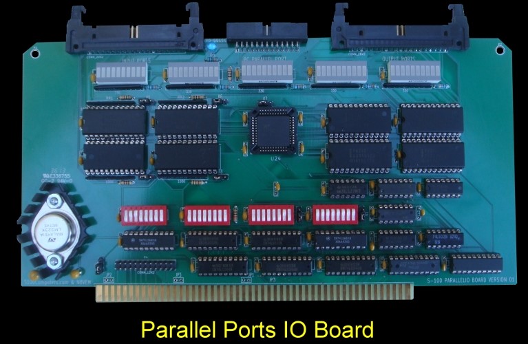
The Final Parallel Ports IO Board.

The final "production run" of this board is now completed and people have received boards.   Some minor tweaks of the above prototype board were made. In particular we reassigned the first LED Bar to display the bit output data of the Printer Port. We also added better Silk Screen labeling. The final schematic and board layout are shown at the bottom of this page. 

Here is a picture of the final Parallel Ports IO Board:-
    
  Production Run-2
        
Step By Step Building The Board.
This is a relatively easy board to build and get working. You will need a printout to the board's schematic and chip/jumpers diagrams, both available at the bottom of this page.

The first step is to examine the board carefully for scratches or damaged traces. Use a magnifying glass if need be. The quality of the boards we get is excellent. I must have done 36 by now, never had a problem, but there is always a first time. A broken trace is almost impossible to detect by eye on a completed board.

Next solder in all the required IC sockets, resistors, resistor arrays, capacitors, jumpers,  the switches SW1 to  SW4 and the 5 Volt, 3A (LM323K), voltage regulator.  Note there is a +5 volt trace coming from the 5 Volt regulator on the front of the board. To be sure the heat sink does not touch it. It's best to use a mica TO-3 insulator (or put a nut washer - one each, between the heat sink and board). Finally be sure to check these regulators before inserting them. Recently I had 3 individual units in two separate lots from Jameco deliver 0 volts with an 8 volt input).

Do not yet add the five LED bars. BTW, the LED bars can either later be soldered directly to the board or inserted in 20 pin sockets.  I prefer the former.  Be sure you put the resistor arrays in with the correct orientation of pin 1.  Check their values before  soldering (they are difficult to remove). 

For prototype boards I generally use "double swipe" IC sockets. For a critical board like this I prefer to use "Machine Tooled" IC sockets.  However they are more expensive and you have to be particularly careful not to bend the IC pins. 

Check the voltage to sockets on the board is about 5V by placing the board in your S-100 system using an extender board. With no load you will typically get between 4.9 and 5.1 Volts.  BTW, your system should boot and run correctly with its Z80 CPU. If not, you have a serious solder bridge somewhere on the board.  Before you do anything else with a magnifying glass go over every socket on the board and examine for a proper solder joint. I like to "reheat" each joint just to be on the safe side. The silk screen/varnish on these boards us quite thick. It's easy not to have a good solder joint for the ground pins.  Double check.   Extra time here will save you hours later!

We will now build the board up in functional steps. Avoid the temptation of adding everything at once and popping it into your S-100 box. Step by step is faster in the end -- trust me.

First add the LED D1.  The color choice is up to you. I use always use a Blue LED for board select in my system.  To check you have the LED orientated correctly insert in the board hole temporally bring pin 6 of U14 to 5Volts. The LED should light up. Only then solder in place.  Here is a picture of the board at this stage:
  
  After Adding LED
    
Now add all the IC's except the 8212's and U24. We will first get one 8212 chip to output to a port and light up an LED bar.
Switches SW1 and SW3 determine the base port address for the 8212's.  I will use the address range 04H-07H in this example.

So SW1 will have all switches closed (high address lines 0's).
SW3 will also have all switches closed except #7. This will correspond to 0000001x binary.  See here to understand how this switch/addressing circuit works.  
Jumper K1 1-2 and K4 2-3.

Using your Z80 monitor and logic probe, output any value to port 04H. U15 pin 3 should pulse low and U11 pin 8 should pulse high.
Port 04H will address 8212 U6. So insert that chip in its socket.
Repeat the above output to port 04H test.  Pin 13 of U6 should pulse high.
Next insert a LED bar in the position labeled "BAR4". Do not solder in place yet. Pin 1 of these bars is the lower left hand corner (like all IC's on the board).
Output to port 04H the value 0FFH.  The left most 8 LED bars should light up.
Here is a picture of the board at this stage:-
   
  Port 04 Output
  
  
Output to port 04H the value 0H, all of the LED bars should go off.  If you are not using sockets solder the LED bar in place.
Next add the remaining output ports 8212's (U7, U8 and U9) and the LED bars BAR2, BAR5 and BAR3.
Do the same monitor output test for ports 05H, 06H and 07H.

Next we will insert the input ports section. We will start with input port 04H (U1) so insert an 8212 in that socket.
Install jumpers K5, K6, K7 and K8 all with the jumpers in the 1-2 position

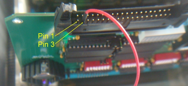
Carefully ground pin 3 of the input socket P7.  Here is a picture:-
 
  Grounding Pin 3
   
  
With your Z80 monitor input port 04H. You should get a value 01111111B.  Carefully change the jumper on P7 and check all 8 bits for this port. Use the schematic to identify the relevant pins on P7.
 
Next repeat this process for the other 3 input ports (05H, 06H and 07H). 

Next we will add the PC Printer Port. Before we add the ST78C34 printer port chip (U24), we have to unfortunately make three small corrections to the board.  As it stands the ST8C34 chips CS* pin 22 is the wrong polarity coming from U11 pin 10. The signal should come from U15 pin 6 (or U11 pin 11).  This is easily corrected by placing a wire jumper on the back of the board connecting U24 pin 22 to U11 pin 11.  However me must also cut the current connection between U24 pin 22 to U11 pin 10.   We do this by using a sharp blade to cut the trace on the front of the board.  It's very important to cut the correct trace.  The cut is done near the front center of the board as shown here as Cut 1:-
  
  Cuts-2

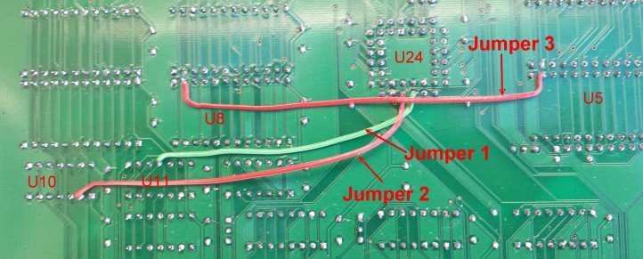
Be sure not to cut the other horizontal trace directly above it.   After this is done turn the board over and solder in the wire jumper as is shown in this picture (green wire, Jumper 1).  Double check to make sure you have the right connections.
  
  Jumpers-2

Pin 22 of U24 is the third pin on the bottom row from the right hand side. 

The second correction is to change the polarity of the chips Reset Pin (#24).  This is a chip active high input. The S-100 bus is active low.  We need to provide a high reset signal to the ST78C34 (U24), and yet at the same time retain the low reset signal to the 8212's.  Providing the high reset signal to U24 can be done by connecting pin 2 of U10 to pin 24 of U24.  Unfortunately however pin 24 of U24 is also connected to the reset signals of U5 and U8. See here:-
  
  Cuts-3

So we must also on the front of the board make two further cuts to isolate U24's pin 24. These are shown as Cut 2 and Cut 3 in then picture above. Be very careful what you cut. If possible use a new blade. A single swipe is usually all you need.  If you have not added components to the board make the cuts first.

Finally we must hook U10 pin 2 to U24 pin 24, jumper 2 above.
Lastly we need to bridge across pin 14 of U5 to pin 14 of U8, jumper 3 above. 

That's it, the resets signals should now be correct for both types of I/O ports.

Next insert the ST78C34 chip.  With most PLCC sockets it can only go in one way. 

For testing I use port 0C0H. (A Z80 does not have 16 bit port addressing ability) .
So for SW2 we will have all switches closed (high address line, all set to 0's).
SW4 will also have all switches open except #2 and #3. This will correspond to 1100000x binary.  Jumper K3 1-2.
Insert an LED bar in the position "BAR1".

Now if you output to port 0CH the value 0FFH all the bars should light up.  Outputting to the same port 0H should turn them off.
Finally check the appropriate pins on P5 to check the signals are correct.  

Next connect up a PC-port compatible printer. This would normally be a DB-25 socket connected via a ribbon cable to the 26 pin header or socket at the center top of the board.  Make sure you use a "standard" printer cable with the pins assigned as shown in the schematic for socket P5 and outlined above.

A simple test to send the letter "3" to the printer (from our Z80 monitor) would be:-

QOC2,08        ;Initialize the chip
QOC2,0C

QIC1              ;Should see 11011111 if printer is selected, ready, with paper etc.

QOC0,33        ;Send Hex value of "3"

QIC1              ;Should see 11011111. Bit 7 indicates printer in not busy

QOC2,0D        ;Pin 1 of P5 should go low. This is for the printer strobe signal
QOC2,0C        ;Pin 1 of P5 now goes back high.


Depending on the printer, the character may be printed right away of if you are using a LaserJet printer a while later.  Some printers need a "flush" command to start printing anything less than a page of characters.  (My Z80 Monitor "@" sends this to my HP LaserJet printer).  You can send a Form Feed character to the printer (e.g. a HP LaserJet) by adding the following lines.

QOC0,33        ;Send Hex value of Form Feed
QOC2,0D        ;Pin 1 of P5 should go low. This is for the printer strobe signal
QOC2,0C        ;Pin 1 of P5 now goes back high.


You now have a fully functional board!  Next you have to carefully hook up the ribbon cable connectors at the top of the board to sockets at the back of your S-100 box.  I will leave that up to you.  However it's best  for the PC printer port to use a 25 pin socket and a pinout as shown above.  If you use MSDOS and an 8086 type setup you will probably want to change the printer port to one of 278H, 378H or 3BCH.

Here is a picture of the board with 0FFh sent to all 5 ports on the board:-
   
  All Ports Lit Up
  

A Second Version of the Board.

There was a large demand for this board. A second run of the boards was done.  Here is a picture of that board:-
        
  V2 Board
    
The "V2" version of the board had a few small changes. 

1.    The layout errors mentioned above were corrected. No alterations to the V2 board are required.
2.    The LM323 3 Amp 5Volt TO-3 regulator was changed to the more common L7805ACV 1.5A TO-220 regulator (Jameco #924570)
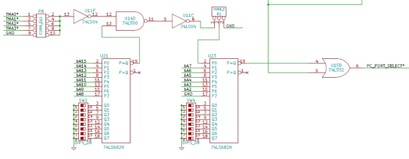
3.    A small circuit was added so that when the Z80 is the bus master 8 bit port addressing for the PC parallel printer port is used.  However when a slave such as an 8086 CPU controls the bus, 16 bit port addressing is used (usually 3CxH).  This allows total PC/MS-DOS compatibility yet does not choke 16 bit CPU's with 8 bit port blocks on every 100H 16 bit boundary.   The circuit to accomplish this is shown here:-
     
  16 Bit Port Selection
     
For 16 bit and 8 bit port selection SW4,1 is left open (high), K1 is jumpered 1-2.  For our 8086 family of boards typically TMA0* is used so jumper P8 1-2.
As an example of the board switch settings.
Switch positions for parallel ports at
04-07H and PC-printer ports C0-C4 (and 3C0-3C4 if TMA0* is low) are shown here:-
     
  Switches
  
If you are using our PDP11 CPU board remember the port range for that CPU is
0-1FFH (FE00-FFFF). So if you activate that board with TMA0 you will be unable to access the printer ports 3C0H-3C4H.  You can either jumper K1 2-3 (8 bit addressing), use a different TMA line or a different port#.
    

Pinout Connectors
This board has a lot of pinout connections. It's fairly important to have some kind of consistency for the connectors at the back of your computer.  The PC-parallel printer port is simple. It should have the pinout connections exactly as in the IBM-PC and as shown above.  The pinouts of the other 8 parallel ports on the other hand is up to you.  As a reference for myself, here is the pinout I use.  I use the company Front Panel Express to layout my port connector plate. Their free downloadable software is easy to use. My back connectors change over time, but here is a picture of the current connector plate slots.
  
  Back Connector   DB-25 Pinouts

The  PC Compatible Printer Port, (the  specialized 44 pin LSI/PLCC ST78C34 chip), can be got from several sources. I got mine from Mouser (Part #: 701-ST78C34CJ44-F).

Bug Report:
Please note the silkscreen labels for the "K1" and "K2" jumpers were flipped on early versions of the board. The correct positions of  the  "K1" &  "K2" jumpers are as shown above.    Boards V2.1 and later have this corrected.

I have replaced resistor R3 (10 Ohms) with a 1K resistor. The former overheats a little.

A Production S-100 Board
Realizing that a number of people might want to utilize a board like this together with a group of people on the  Google Groups S100Computers Forum, "group purchases" are made from time to time.  Contact and join the group if you would like to be involved in this project.  Please see here for more information.

The links below will contain the most recent schematic of this board.
Note, it may change over time and some IC part or pin numbers may not correlate exactly with the text in the article above.


PARALLEL PORTS (V1) BOARD SCHEMATIC     (V1.1  4/22/2013)
PARALLEL PORTS (V1)  BOARD LAYOUT    (V1.1  4/22/2013)

PARALLEL PORTS (V2) BOARD SCHEMATIC   (V3   7/18/2014)
PARALLEL PORTS (V2)  BOARD LAYOUT
    (V3  7/18/2014)
Most current KiCAD files for this board  (S100 ParallelIO-002.zip 11/6/2014)


Other pages describing my S-100 hardware and software.
Please click here to continue...

This page was last modified on 12/13/2017