S100 Computers

Home S-100 Boards History New Boards Software Boards For Sale
Forum Other Web Sites News Index    
  
A 6502 CPU S-100 Board.
      
  6502 CPU Board
INTRODUCTION
None of the major S-100 Bus board manufacturers made a 6502 based CPU S-100 boards.  Nevertheless the MOS (and later WDC), 6502 CPU turned out to be a very popular microprocessor. It was the basis of Apple II and a related chip, the 6507, for the Atari desktop line.  

A number of people saw the need for a "homebrew" S-100 based 6502 CPU board.  However these boards are very rare today.   There is a need for a new S-100 based 6502 CPU board.   Furthermore it would really be nice if such a board could take advantage of the IEEE-696's bus standards to allow the board to co-exist with other CPU's on the bus.  One could for example switch from a Z80 (or 8086) to the 6502 board and back again in software.  Unfortunately I know of no 6502 board that has this capability.  We will try and incorporate this master/temporary master capability in our new board (more on this later, see below). 

The Motorola 6800 and MOS 6502 represented the "other side" of the great software divide for desktop systems in the early PC days.   There was a continuous tug of war between the Intel/Zilog camp and the Motorola/MOS camp.   This later evolved into the PC based 8086, 80286, 80386, 80486 and Pentium based systems. The Motorola camp, Apple/Sun based, evolved into 68000, 68020, 68040 based systems. See here for a brief historical summary.

I have to admit that up until now I have always found myself in the Intel camp, both in terms of hardware and software.   From a hardware perspective there are some very significant differences how Intel/Zilog and Motorola/MOS CPU's talk to the world.  Somewhat oversimplifying, one could say that Intel CPUs assume that external devices are ready to talk to them immediately unless told otherwise (adding wait states).  While Motorola/MOS CPU's assume the opposite, they wait for a "I'm ready to talk" signal unless they are told otherwise -- so called synchronous communications.

When we look at the S-100 bus signals it is clear that it is setup for Intel style chips -- this really has to do with the bus's origin, an 8080 CPU.  To insert a MOS 6502 CPU board therefore on the bus one has to take care shoehorning the CPU signals in carefully.

Nevertheless, Andrew Lynch, Neil Breeden and I decided to have a go at building a new S-100 6502 board.  The first version of this board is a stand alone 6502 bus master S-100 board and is based on a version of a board done some time ago by Rich Leary. Thank you Rich. He is the author of DOS/65 (a CPM like disk operating system for the 6502).  He made the original S-100 6502 CPU as a home brew prototype board.  In this configuration the CPU board assumes it is the only CPU in the bus.  For more information about DOS/65 please see here.
  
Below is a picture of this 6502 CPU board. 
Please note this board is NOT IEEE-696 compatible. It is designed to work in the original IMASI/Altair systems that have (up to) 64K of RAM and utilize only 8 bit I/O ports.   Rich went through each of the original S-100 bus signals and figured out how they could be adjusted for the 6502 CPU.  Please see here for a description of the results.

A second more powerful board that can function as a bus master or temporary master with other CPUs and is IEEE-696 compatible is described later below.


You will notice the board contains its own onboard ROM.  Relatively few support chips are required so there is a large "patch" area at the top of the board where one can add specific features to the board. The schematic for this board can be seen here

Programming the 6502
To the Intel/Zilog programmer the 6502 may appear a little strange.  It has a small number of internal registers. The program counter (PC) is 16 bytes wide,  all the rest hold only one byte. The stack pointer (S) points to a byte on "Page 1", whose address is from 100H to 1FFH and where the last two digits are supplied by register "S".  When a byte is pushed onto the stack, it is written at the address in S, and then S is decremented. Popping a byte from the stack is done in exactly the reverse order, S is incremented, and the byte there is read. The accumulator "A" holds one of the operands in every operation, and most of the processing instructions refer to it. The two index registers "X" and "Y" hold auxiliary numbers used in addressing, and can also serve as temporary storage when necessary. There is also the flags register "P", whose contents are used in making comparisons. The programmer works principally with A, X and Y, and does not usually handle the others (P, S, PC) explicitly.  That's all there is!  Interestingly the original 6502 there in no unconditional branch. You have to use:-      


   CLC      
   BCC   Somewhere


The good news is the 65C02 has a Branch Always (BRA) opcode (and a number of other extra opcodes).   We will use the 65C02 in all our discussions here.  BTW, you also have to be careful about the carry flag with move instructions - it changes with some!

For the 6502 processor, the uppermost six bytes of memory (FFFAH-FFFFH), are the non-maskable interrupt (NMI), reset, and interrupt (IRQ) vectors, in that order. They should point to the routines used to handle each event. An interrupt, whether NMI or IRQ, begins (if enabled) at the end of the current instruction. The PC (which is pointing to the next instruction) is pushed on the stack, followed by the flags register
P. Upon executing RTI (Hex code 40H), the exact reverse occurs. On a jump to subroutine, JSR, only the PC is pushed on the stack, but it points to the last byte of the JSR, not to the next instruction. Upon RTS (Hex code 60H), the first thing to do is to pull the PC and increment it.

The interrupt disable flag,
I, is bit 2 in the flags register. Clearing it, with CLI (Hex code 3AH), permits the processor to recognize interrupts (the opposite to Intel terminology). Setting it, with SEI (Hex code 4EH) causes the processor to ignore the state of the IRQ pin.  Somewhat unusual from an Intel prospective, the decimal flag, D, is bit 3 in the flags register. Clearing it, with CLD (Hex code D8H) means the processor will do arithmetic normally, but if you set it, with SED (Hex code F8H), you will get BCD arithmetic. You must clear the carry flag with CLC (Hex code 12H) before doing an add, and set it with SEC (Hex code 38H) before doing a subtraction, since these instructions normally either add carry, or borrow from carry, automatically. These three flags are the only ones you can both set and clear independently.

The 6502 uses the first 255 bytes of RAM as registers. It is very important you understand the difference between a number, a "page zero" RAM location and a pointer to 16 bit memory in Page zero when programming the 6502.

One very good book by Lance Leventhal I found that describes how to program the 6502 and can be seen here.   I highly recommend you read this book if this is your first time with the 6502.


The Free Run Test
In bringing up this board one nice thing one can do after adding all the components except the eight 74LS541's (U3, U7, U2, U6, U5, U20 and U30), is run the CPU in "Free Run" mode.   In this mode we take advantage of the fact that the NOP instruction for this CPU is 0EAH. So if we jam 0EAH on the CPU's eight data pins it will continuously loop through its address range 0 to FFFFH.  We jumper our board so the CPU's pins are configured as shown below.  This will cause the 6502 will continuously cycle its address lines after each CPU reset.
    
Free Run CPU
Free Run Board Picture
   6502 CPU board in "Freerun" test mode 
 
  
This is a very simple but useful test for this board. It gives you some assurance your CPU is OK, the reset circuit is working OK and your boards clock generator is working fine.  However you have to be careful to temporally tie high a number of the CPU's input lines as shown above.   The easiest way I found to ground the CPU data lines was to insert a set of jumper pins in an IC socket and insert it in position U40 on the board.  The appropriate data pins and tie these to ground or high.   Checked all the pins in the 6502 socket for the correct voltages before adding the CPU chip itself.  You don't want to have the CPU trying to pull a grounded line high.

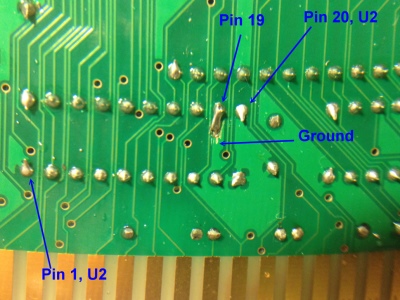
Next I added the 74LS541's and 2732 EPROM chips to the board.   There is one small error on this board. Pin 19 of U2 is unconnected. At the back or the board you must connect this pin to ground with a short jumper as shown here:-
  
  Pin 19,U2 Correction
    
What to code our PROM with.  To answer this you must appreciate that the 6502 CPU starts up at 0FFFCH in RAM  -- every time, no exceptions.  At this location in RAM it expects to find a two byte JMP to its boot up code typically a monitor program in lower regions of the PROM.  Our first test code will be real simple, a loop to continuously output to a port a byte value of 33H ("3").   We will locate the ROM at 0F900H in the CPU's address space.  Here is the code we use:-

Test Port Output Code

The above code illustrates one major difference between the Intel and MOS family of chips. On the 6502 there are no special control/status signals for the control of I/O ports. As far as the 6502 is concerned an I/O port is just another memory location. In order to emulate the S-100 bus port I/O status signals we set aside a block of the 6502's RAM address space for port I/O. The easiest block to use in hardware is the 64K space from F800H to F8FFH.  So if the address lines A8-A15 are all within this range, pin 19 of U13 (a 74LS682, see here) goes low activating the S-100 bus port IO signal (for the S-100 bus signals SOUT or sINP).  Port 01H is my Propeller driven Console I/O board data input port.  An output of 33H to port 01H should place an ASCII "3" character on the screen.  Remember now, no 6502 code in the PROM from F000H to F8FFH will be visible. The PROM monitor code must start from F900H-FFFFH. The 6502 expects the last 6 bytes to contain:-

FFFFAH  –  NMI Vector LS Address
                  
FFFFBH  –  NMI Vector MS Address
                   
FFFFCH  –  Reset Vector LS Address
                  
FFFFDH  –  Reset Vector MS Address
                  
FFFFEH  –  IRQ/BRK Vector LS Address
                  
FFFFFH  –  IRQ/BRK Vector MS Address

 
We will only use the Reset vector initially in our monitor software.

Here is a picture of the board with the necessary chips to achieve this test.  You can see the console is continuously receiving the byte value 33H. 
       
  letter 3 on CRT
         
This is a critical test for the circuitry of the board because it is the first time the CPU is talking to the outside world and utilizing the S-100 bus. 

Before loading the 6502 monitor program I wrote (see below) I used the a short program to input a value from my IOBYTE port on the SMB board and display the contents as ASCII on the console.  By varying the IOBYTE switches different characters should appear on the screen. This test program can be see here.

Assembling 6502 Programs.
There are many good assemblers for the 6502 CPU.  I have just started using the TASM assembler written some time ago by Thomas Anderson of Squak Valley Software. Its excellent. It can be downloaded here. It even runs in 64 bit Windows 7.

The next step was to write a simple 6502 specific ROM monitor.  My goal was to model it after the 8086 monitor I wrote.  I wanted to use all the same menu options -- to keep life simple. I should point out that there are a number of excellent well tested 6502 monitor programs, check the web. The 6502 Monitor program can be seen here and downloaded here.  You will note that this monitor is too large to fit between F900H and FFFFH. I have changed the board settings so the I/O address space starts at F000H-F0FFH and the ROM code starts at F100H to FFFFH. 

Note, if you are using a 28C64 type EEPROM you need to place the 4K 6502 monitor in the top half of the 8KX8 EEPROM.  Please review the write-up
here if you need more help on this topic.


A Description of the Board Jumpers.
The  board contains a few of important jumpers that determine how it functions. Most will not need to be changed once the system is running but it is very important they are configured correctly.  In no particular order:-
    
Jumper    Function 
JP4,JP5,JP6,JP7 Used only if the board does not generate these signals with a front panel.
K1 1-2 accept NMI interrupts from the bus
P10 Normally 1-2 and 3-4
P2 & P3 Normally 7-8 in both cases.
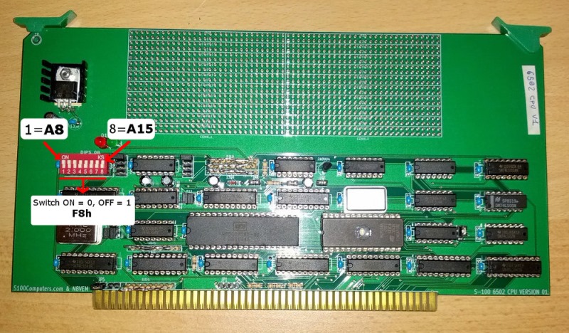
SW1 This switch determines the start of the EPROM & IO address space.
P11 1-2 and 3-4  IF these two signals are not provided elsewhere on the bus.

Closing a switch connects the corresponding 74LS682 comparator pin to GND, meaning a 0 bit in the address. As we saw above, the 6502 resets in high RAM.   If you use an EPROM/IO address space starting at F800H to FFFFH and a 2732 EPROM the switch setting will be F8xxH, so left to right:-

closed, closed, closed, open, open, open, open, open

The leftmost switch compares to address line A8, the rightmost to A15.  Please see the picture below:
  
  V1 Jumpers

  
If you use an EPROM/IO address space starting at F000H to FFFFH and a 2732 EPROM the switch setting will be F0xxH, so left to right:-

closed, closed, closed, closed, open, open, open, open

Setting the switches to F800H puts the I/O address space in the range F800-F8FF, and the EPROM address space in the range F900-FFFF. Keep in mind that the first 256 bytes of the EPROM space are invisible to the CPU (as mentioned, this space is overlapped by the I/O range), keep in mind also that  the I/O boards need to be configured to have their address fall into the correct I/O range: for example, to set the Console I/O board for the F800 address one must configure the following switches on it, from left to right:

Bank 1: open, open, open, open, open, closed, closed, closed
Bank 2: open, closed, closed, closed, closed, closed, closed, closed

A Production 6502 IMSAI/Altair Style S-100 Board.
The first Bus Master 6502 board is now longer available as a bare board. If the was a need, a group purchase could be again organized on the Google Groups S100Computers forum.

A IEEE-696 Compatible S-100 6502 Master/Slave CPU Board.
Realizing that a number of people might also/later want to utilize a board with master/temporary bus master capability as described above, I used the above board as a basis for designing a IEEE-696 compatible 6802 S-100 board that could act as a bus master or with other CPU boards on the bus (e.g. Z80 or 8086) act as a temporary master.    Converting a board over like this is not as simple as it sounds.   The process of transferring control of the bus from one CPU (or DMA controller) to another is clearly defined in the IEEE-696 specs, and has to be done carefully with proper signal "handshaking".    I utilized the by now, well tested, circuit I used for our 8086 board and spliced it into the circuit of this CPU board.   Being a "non Intel" style CPU chip, the splice is not perfect.   For example, on the 6502 there is no equivalent signal to the Intel Interrupt Acknowledge signal (S-100 pINTA).  So an 8259A could wait forever for a response to its INT signal being placed on the bus.  The simplest approach for interrupts with this CPU is just put a PIC like an 8259A in "poll mode" and read its status register after an INT.

The IEEE-696 allows up to 16MG of RAM, so address lines A16-A23 must be pulled low when the 6502 has control of the bus.  Likewise the 6502 is an 8 bit CPU, so all I/O ports we use, (RAM F000H-F0FF), must set the upper 8 address lines to 0.  The  schematic of the resulting 6502 prototype board can be seen here

We have just completed the testing of this board. Here is a picture of the board:-

master slabve 6502 prototype

The board has checked out fine and behaves identically to the initial board described above. However in this case you can run the CPU is slave mode. For example you can boot your system up with your Z80 and switch over to this 6502 CPU board (and back again later if desired). Any program placed in RAM by the Z80/CPM can be picked up by the 6502 CPU.  This greatly helps writing software like a 6502 disk operating system.

We went on to construct a second 6502 Prototype board to correct some of the minor errors in the above board. Here is a picture of that board.
6502 M/S Final Prototype
 
This board can be configured as a stand alone (Master) 6502 S-100 bus CPU board or as s slave CPU board where it will reside in the bus transparently until it is activated. Please excuse the one wire patch and two empty sockets. They will be removed on the final board.

Remember if you are using a 28C64 type EEPROM you need to place the 4K 6502 monitor in the top half of the 8KX8 EEPROM.  Please review the write-up here if you need more help on this topic.


The Final Master/Slave 6502 CPU Board.

The final (V3) of this board is now completed and people have received boards.   Some minor tweaks of the above V2 prototype board were made. In particular we reassigned some gates and removed  empty sockets. This allowed considerable trace optimization. The final schematic and board layout are shown at the bottom of this page. 

The board in my 22 slot S-100 bus runs rock solid at 4 MHz. Some day I may try tweaking the system. The 65C02 CPU I have is rated for 4MHz, faster chips might be interesting. 

Here is a picture of the Final 6502 Master/Slave CPU Board.
  
Production 6502 Board
   
Step By Step Building The Board.
Since for many this board may be their first venture into putting a Master/Slave setup in their S-100 bus I will go into some detail as to how to get it up and running.  You will need a printout to the board's schematic and chip/jumpers, both available at the bottom of this page.

The first step is to examine the board carefully for scratches or damaged traces. Use a magnifying glass if need be. The quality of the boards we get is excellent. I must have done 35 by now, never had a problem, but there is always a first time. A broken trace is almost impossible to detect by eye on a completed board.

Next solder in all the required IC sockets, resistors, resistor arrays, capacitors, jumpers, the 2 and 4 MHz Oscillators,  the SW1 and SW2 switches and the 5Volt, 3A (LM323K), voltage regulator.  Be sure you put the resistor arrays in with the correct orientation of pin 1. Check their values before  soldering (they are difficult to remove). 

For prototype boards I generally use "double swipe" IC sockets. For a critical board like this I prefer to use "Machine Tooled" IC sockets.  However they are more expensive and you have to be particularly careful not to bend the IC pins.  If you think you will be doing a lot of EEPROM burning you should use the Low Profile ZIF sockets (e.g. Jameco #102745) for the EEPROM socket.  The two clock oscillators should have their own special sockets (e.g. Jameco #133006).

Check the voltage to sockets on the board is about 5V by placing the board in your S-100 system using an extender board. With no load you will typically get between 4.9 and 5.1 Volts.  BTW, your system should boot and run correctly with its Z80 CPU. If not, you have a serious solder bridge somewhere on the board.  Before you do anything else with a magnifying glass go over every socket on the board and examine for a proper solder joint. I like to "reheat" each joint just to be on the safe side. The silk screen/varnish on these boards us quite thick. It's easy not to have a good solder joint for the ground pins.  Double check.   Extra time here will save you hours later!

We will now build the board up in functional steps. Avoid the temptation of adding everything at once and popping it into your S-100 box. Step by step is faster in the end -- trust me.

We will first build this board as an S-100 Bus Master.  So remove any other CPU(s) in the bus. To be on the safe side remove all boards except your SMB/Front panel (if you have one), a RAM board and whatever board(s) you use for console I/O.

First add the 4 LED's.  The color choice is up to you. I use Blue for board select, Red for ROM access, Green for I/O cycles and Yellow for wait states.  To check you have the LED orientated correctly insert in the board hole temporally ground the appropriate pin on U26 or U41. The LED should light up. Only then solder in place.  Here is a picture of the board at this stage:
 
  before Chip Additions

 
Jumper P7 1-3, K3 1-2, K2 1-2 K1 1-2 and jumper JP11 (not P11).
Add U24, U26 and U18.   Insert into the S-100 bus. LED D4 should light up.
If not already added add the 2 & 4MHz Oscillators.
Add U27, U11  and U20.  Jumper P11
Add U4, U22 U42 and U36.
If your system does not have a SMB or front panel add Jumpers JP4, JP5 and JP6.  Leave open if some other board/circuit takes care of the S-100 bus signals POC and reset.

Add U9, U30 and U16.  Add jumper K7 2-3,  make sure the jumper does not contact the 2MHz metal oscillator.
Add jumpers JP16, JP17, JP18 and JP19.

Make up the "freerun" jumper socket described above and insert into socket U40.   This will place the opcode EA on the 6502 data bus.  In this mode we take advantage of the fact that the NOP instruction for this CPU is 0EAH. So if we jam 0EAH on the CPU's eight data pins it will continuously loop through its address range 0 to FFFFH.  Be sure NOT to  add U5 -- leave that socket empty.
  
  U40 Jumper

Before inserting the CPU in the board check that the 6502 pins  (U1)
26, 27,28, 29, 30, 31, 32, 33 are high, high, high, low, high, low, high, low.

Insert the CPU in U1.  On power up the CPU address line A15 (25) should pulse continuously.   Do not go further until you get this to work.
  
  A15 test

Add U3, U28, and U6. Repeat the above CPU freerun test. The address lines should continuously change if you have a SMB or front panel -- so fast in fact they appear as 888888's.

Add U7, U12, U31 and U32. repeat the above test.

Add U2 and U13.  Jumper P2 1-2, 3-4, 5-6 & 7-8  and P3 1-2, 3-4, 5-6 & 7-8.

Repeat the freerun test. Pin 12 of U16 should pulse (as the CPU cycles through the ROM space).

Next add the wait states circuits.
Add U19, U29 and U33.  Repeat the freerun test.  With all switches open LED D6 should not flash.

Add U23 and U17. Add jumper JP12, JP13  
Note if another S-100 board is pulling INT* or NMI* high you don't need these two jumpers.
Add K4 2-3.  No interrupts  are use initially with this board!

Running the freerun test now should allow you to stop and/or single step the CPU if you have a SMB or front panel.
Add U41. LED D2 should flash in freerun mode if wait states are applied via SW2. 
Next remove the socket jumper in U40 and add the 74LS373 chip.  Also add U5.
Here is a picture of the board at this stage:-
  
  Before EPROM addition

 
Burn a 28C64 EEPROM with the 6502 monitor and place it in U39. 
Add jumpers JP14 1-2, P31 3-4 and leave JP15 open.

Insert in the S-100 bus the monitor should signon your board should be functional.  It will be running as a bus master CPU.

Next we will reconfigure the board to work as a slave CPU board where it will be dormant unless activated by a bus master (normally a Z80 board).  In order to implement this pin 1 of U16 must be grounded.  We can do this by outputting to a port on this board or by inputting from a port on another S-100 bus board. For example Port EDH on our SMB.   In either case via jumpers on P5 pin 1 on U16 will be taken low. This triggers the master/slave handshake/changeover of the CPU's using the circuit around U12 and U25.  This circuit is explained in more detail here.

The onboard (configurable port) is implemented by adding U8, U10, U43 and jumpering K6 2-3.  We jumper P30 1-2 so bit 0 (low) will activate the 6502 board.   Lets use port 99H. 
So we jumper P10 3-4, 5-6, 11-12,13,14. The other jumpers on P10 are left open.

If we output to port 99H a value of 0H via our monitor pin 1 of P5 (TMAXPU) should go from high to low.  Please note there is currently a bug in my monitor code that allows port addresses with digits 0-9 (and not A-F). 

OK, now lets add the slave switch-over circuit. 
Add U8, U10 and U43
Add U21 and U25.    Jumper P7 2-4, add JP10.
Jumper K2 2-3, K3 2-3 and K1 2-3.
You may want to add JP8 and JP9 if no other S-100 boards are pulling these lines high.

If you are going to use the above onboard port to flip CPU then jumper P5 1-2.  If you are using another S-100 board then use the appropriate jumper on P5.

If you reinsert the board into the bus it should not now "light up"  i.e. no LED's on.  Power down and insert your Z80/master CPU. Activate your master/slave switch-over port. The 6502 should become active and take over the bus.  With the appropriate software you should be able to go back and forth between the two CPU's.

If somebody out there has time,  could they put together a parts list for this board.   I will publish it here. 
The board uses standard parts available from the likes of Jameco, DigiKey, Mouser etc.

A Description of the Board Jumpers.
The  board contains a number of important jumpers that determine how it functions. Most will not need to be changed once the system is running but it is very important they are configured correctly.  Also note the orientation of pin 1 will vary, always consult the board layout diagram.  In no particular order:-
     
Jumper    Function 
JP4,JP5,JP6,JP7,JP19 Used only if the board is to act as a bus master.  Generates Power On reset etc.
JP8 Use only if no other board on the bus pulls up the S-100 HOLD signal
JP9 Use only if no other board on the bus pulls up the S-100 HLDA signal
K2, K3 Normally 2-3. Use 1-2 if board is a bus master.
K1 Normally 1-2 if slave. 2-3 if master. Controls when 6502 Active LED (D4) lights up
K5 Normally 1-2.
K4 Normally 2-3.  Determines how and what  S-100 bus interrupts will triggered the CPU
P11 Use only if no other board generates the S-100 2MHz clock signal when the 6502 is active
JP11 Use only if no other board generates the S-100 MWRT signal when the 6502 is active
SW1 Sets number of wait states for onboard EEPROM (0-8). I use 0 wait states, so all switches open for 4MHz CPU
SW2 Sets number of wait states for bus I/O and INTA cycles (0-8). I use 0 wait states, so all switches open for 4MHz CPU
P7 Normally set 2-4. Use 1-3 if board is bus master
JP12, P13 Use only if no other board on the bus pulls up these signals when board is active
JP14,P31,JP15 These pins must be carefully selected for different EEPROM and EPROM types. (For 28C64:- Close JP14,  P31-2-3, JP15 Open)
P30 Normally 1-2,  This selects the port bit that activates the CPU in slave mode. If 0, board is activated.
P2 & P3 This selects where the onboard EEPROMS will reside in the CPU's 64K address space
P10 This selects the S-100 I/O port that is used to activate the CPU in slave mode.
P34, P35, P36 These jumpers are to pull up the S-100 bus Interrupt and DMA lines IF no other board on the bus pulls them high.  Normally they are not jumper (they are pulled up by the Z80 master CPU).  It is essential multiple boards do not pull them high.
P5 Determines how master/slave switchover is accomplished. 1-2 the onboard port, else another board lowers a DMA line
K7 Normally 2-3. Fine tunes when the S-100 bus sSTVAL* is sent
JP1,JP2, JP3 These are jumpers that allow you to utilize extra board ground lines as defined in the IEEE-696 specs.  Nor required, do not use with older S-100 systems

Also please let me know if you notice any errors in the construction notes.

Please not that not all 6502 CPU's are the same.  There appears to be some subtile signal differences between those produced by different manufacturers.  For this board make sure you use  the Rockwell R65C02P4E CPU chip.  There are reports for example of people unable to access RAM with the Western Design Center W65C02C chip.

A Production Board
Realizing that a number of people might want to utilize a board like this together with a group of people on the  Google Groups S100Computers Forum, "group purchases" are made from time to time. 
Please see here for more information.


The links below will contain the most recent schematic of these boards.
Note, it may change over time and some IC part or pin numbers may not correlate exactly with the text in the article above.


6502 Macro Assembler  (1/15/2012)

MOST CURRENT 6502 CPU (IMSAI/Altair STYLE)   BOARD SCHEMATIC    (V1, FINAL, 1/15/2012)
MOST CURRENT 6502 CPU  (IMSAI/Altair STYLE)  BOARD LAYOUT  (V1, FINAL, 1/15/2012)


MOST CURRENT 6502 CPU (V3 - IEEE-696  BOARD) SCHEMATIC  (V3, FINAL, 8/10/2013)
MOST CURRENT 6502 CPU  (V3 - IEEE 696 BOARD)  BOARD LAYOUT  (V3, FINAL, 8/10/2013)
Most current KiCAD files for this board  (S100 6502 V2-003.zip 11/5/2014)


Other pages describing my S-100 hardware and software.
Please click here to continue...

This page was last modified on 11/30/2017