An SPI Master Controller Interface Demo using a Cyclone IV FPGA.
Here we
will improve on our earlier FPGA SPI interface and use it to communicate with a variable
number of of data bits. This can be 8, 16, 24, 32, 40 or 48 bits. Long SPI
continuous data streams are for example requires to interface with SPI SD Cards. These require 6 byte commands.
Unlike the I2C interface the SPI
clock cannot be stretched. You must have all the data bytes setup before you
start. The good news however is for most SPI chips, you can delay getting
data to the chip if you just hold CS* (Chip select) low until everything is
done.
If you have not done so already, please read the introduction to the
SPI interface before going further.
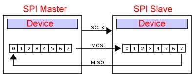
To recap, to begin communication, the bus master starts the clock, using a frequency
supported by the slave device. Typically this can be in the 100's of KHz range.
The master then selects the appropriate slave device by lowering that slaves SS
input. If a waiting period is required, such as in for an analog-to-digital
conversion, the master must wait for at least that period of time before issuing
clock cycles. This has to be agreed upon in the programming software. The master then sends a bits on the
MOSI line and the slave reads them. At the same time
the slave sends bits on the MISO line to the master. This sequence is maintained
even when only one-directional data transfer is intended. I.e to read a byte you
must send a byte. Its important to appreciate two things.
1. The sending and receiving data to/from the slave is completely
linked. There is just one loop like circuit with two shift registers (see
below).
2. The actual data format is completely determined by the
software in the master and slave. The number of bits transmitted can be 8,
16, 32, 48 etc. In theory any number.
While the most common format is data are 16 bit packages, and that is what we
used in our first FPGA SPI example.
There are many devices
that require more data bytes/commands.
What is needed is a more generalized SPI interface with no limit on the number
of outgoing or incoming data bytes. Such an SPI interface can be used for
numerous SPI chips.
There are numerous examples of building an FPGA SPI interface on the web.
As a beginner, frankly I found a number of them overly complex and/or confusing.
Fortunately I discovered a simple and well explained example by Scott Larson
here.
This one is a more generalized form of his earlier
two input byte interface. That demonstration which I used for the
V1 FPGA
Board was quite specific for a SPI device that had a two byte data input and
a single byte output. While it works fine for our MCP42010 chip, I wanted to
explore a more generalized data I/O FPGA module. The module below modifies
Scotts code to have a single byte input and output but one where we can send multiple
bytes by controlling separately the chip select (CS*) line. For most SPI chips
you can send multiple bytes in any time frame you like so long as you keep CS*
low. That is what we do here. I used
Scott's VHDL code.
I actually don't use his "Continuous mode flag" -- this would require a FIFO to
keep the module input fed. Instead I simply control CS* separately keeping it
low until all bytes are sent. It took me a while to realize this
approach. A big help was an article by Ben Martin using an Arduino chip to
program a SPI EPROM. See
here. This program was invaluable because it allowed me to write known
data to the SPI PROM and check it read back correctly.
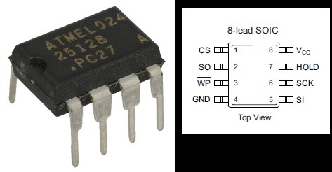
As an example we will read and write to a 128K SPI Serial 128k
AT25128 Atmel EEPROM.
This is a 8 pin chip with the following pinout.
Remember unlike the equivalent I2C chip
there is a separate data in and out pin. Chip/device addressing is done in the
software. To program the chip WP* must be brought high. This chip in fact has an
internal addressable control register which allows you to write protect pages of
the chip as well as other things. We will not use that facility in this
simple example.
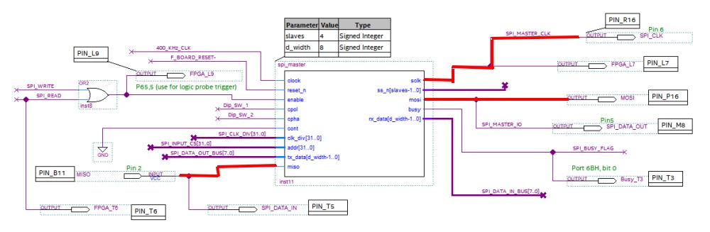
Here is the core FPGA module.
You will note that now the module now has single 8 bit input and output lines.
Gone are the separate two 8 bit "CMD"
and "Data" bus
input lines. It is not as easy to write data to the PROM from
the Z80 Monitor commands one by one. So load the I2C.COM
file into RAM at 100H using a program like XModem and the 'X' command of the
Z80 Master monitor and run it at 100H.
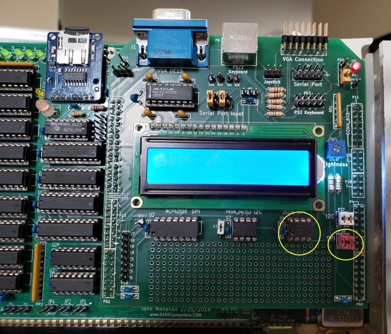
Set
Dip_SW1 &
Dip_SW2 to Closed
Position. (SW2 does not seem to matter, but SW1 (CPOL)
must be Close, i.e.
FPGA_G11 LOW).
If
set correctly the LEDs L2 & L3 on the WaveShare Board should be on.
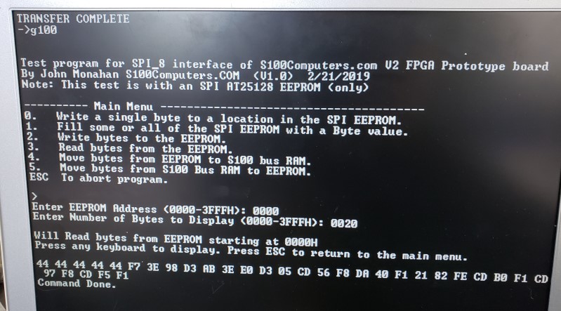
Here is a picture of the signon menu running at 100H in RAM.
Here is the core SPI write Z80 code.
BYTE_WRITE: ; >>>>>>>>>>>>>>>>>>> START CORE BYTE WRITE ROUTINE
>>>>>>>>>>>>>>>>>>
LD A,EEPROM_CS_LOW ; ADDRESS IN (START_STORE), Data in (DATA_STORE), NOTE HL++
on return
OUT (SPI_CS),A ; Select EEPROM
LD A,INST_WREN ; Set Enable WR latch
OUT (SPI_DATA_OUT),A
CALL
WRITE_SPI ; Send Write pulse (Port 6B)
LD A,EEPROM_CS_HIGH ; Deselect EEPROM
OUT (SPI_CS),A
LD A,EEPROM_CS_LOW ; Select EEPROM leave low (Seems to be required each time)
OUT (SPI_CS),A
LD A,INST_WRITE ; Read EEPROM instruction
OUT (SPI_DATA_OUT),A
CALL
WRITE_SPI ; Send Write pulse (Port 6B)
LD HL,(START_STORE) ; Store address in PROM HL
LD A,H
OUT (SPI_DATA_OUT),A
CALL
WRITE_SPI ; Send Write pulse
LD A,L
OUT (SPI_DATA_OUT),A
CALL
WRITE_SPI ; Send Write pulse
LD A,(DATA_STORE) ; Get Data Byte
OUT (SPI_DATA_OUT),A
CALL
WRITE_SPI ; Send Write pulse
LD A,EEPROM_CS_HIGH ; Deselect EEPROM
OUT (SPI_CS),A
INC HL ; NOTE [HL] is incremented in BYTE_WRITE on return
LD (START_STORE),HL
LD A,EEPROM_CS_HIGH ; Deselect EEPROM
OUT (SPI_CS),A
RET
WRITE_SPI:
IN A,(SPI_STATUS) ; Wait until busy is low
BIT 0,A
JR NZ,WRITE_SPI
OUT (SPI_WRITE),A ; Send Write pulse (Port 6B)
PUSH HL
LD HL,100
DELAY:
DEC HL ; Allow time for Busy to rise
LD A,H
OR A,L
JR NZ,DELAY
WAIT1:
IN A,(SPI_STATUS) ; Wait for busy to go back low
BIT 0,A
JR NZ,WAIT1
POP HL
RET
One thing to keep in mind with this EEPROM is after
you write a byte you must allow the chip some time to do so. You will see a call
to "DELAYX:" within the Z80 code to do this.
The SPI chip actully has a status register that can be read to determine if it
is busy writing (see the datasheet). However for most
purposes we can just insert an overkill time delay. BUGS
No bugs reported to data.