
| Home | S-100 Boards | History | New Boards | Software | Boards For Sale |
| Forum | Other Web Sites | News | Index |
 |
 |
 |
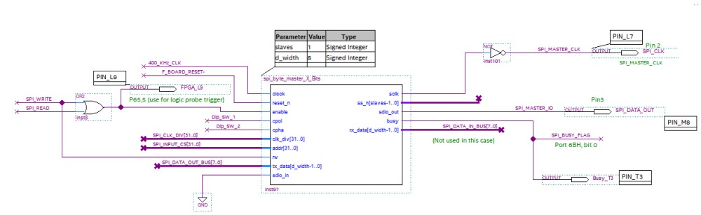 |
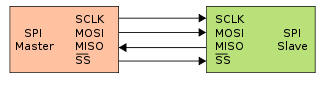
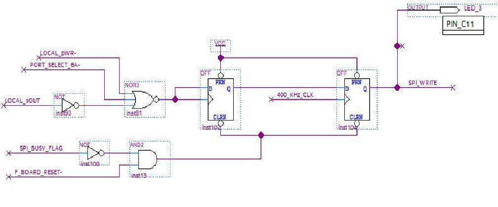
| clock | 1 | in | System clock. |
| reset_n | 1 | in | Asynchronous active low reset. |
| enable | 1 | in | High: latches
in settings, address, rw, command, and data to initiate a
transaction Low: no transaction is initiated. |
| cpol | 1 | in | SPI clock polarity setting. |
| cpha | 1 | in | SPI clock phase setting. |
| clk_div | 32 | in | Speed setting. The integer input is the number of system clocks per 1/2 period of sclk. |
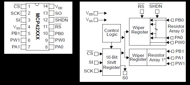
| addr | 32 | in | Address of target slave. Not used here. |
| rw | 1 | in | High: the transaction is a write, Low: the transaction is a read. |
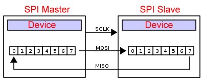
| tx_data | 8 | in | Data to transmit. |
| sclk | 1 | buffer | SPI clock. |
| ss_n | 32 | buffer | Slave select signals. Not used here. We address CS* seperately. |
| sdio | 1 | inout | Serial data signal. |
| busy | 1 | out | Busy / data ready signal. |
| rx_data | 8 | out | Data received from target slave. Not used here |
 |
 |
 |
 |
 |
This page was last modified on 07/28/2019