Banner 

HomeS-100 Boards HistoryNew BoardsSoftwareBoards For Sale
ForumOther Web SitesNewsIndex   
 
An I2C Master Controller Interface Demo using a Cyclone IV FPGA.
Here we will construct an FPGA I2C interface and use it to communicate with a common AT24C512 EEPROM using our S100 bus FPGA V2 Prototype board
This I2C device is a simple 521 byte EEPROM which communicates with its host over only a two wire "I2C" connection.

Introduction I2C
The I2C is a synchronous serial communication interface used for short distance communication.  It is primarily used in embedded systems. The interface was developed by Philips/NXP in the mid 1980s. Typical applications include SD cards, EEPROMs and LCD displays. I2C devices communicate in a full duplex mode using a master-slave architecture.  The interface is somewhat similar to SPI  but is a two wire interface and can have multiple masters. Here is a comparison of SPI and I2C:-
   
     IC2   SPI
  I2C can be multi-master and multi-slave, which means there can be more than one master and slave attached to the I2C bus   SPI can be multi-save but not a multi-master. That means there can be only one master attached to the SPI bus.
  I2C is a half-duplex communication protocol   SPI is a full duplex commination protocol.
  I2C has the feature of clock stretching, that means if the slave cannot able to send fast data as fast enough then it suppresses the clock to stop the communication.   Clock stretching is not possible with SPI.
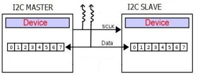
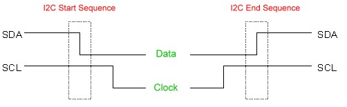
  I2C uses only two wires for the communication, one wire is used for the data and the second wire is used for the clock.   SPI needs three or four wire for communication (depends on requirement), MOSI, MISO, SCL and Chip-select.
  I2C lines require pull-up resistors.   There is no requirement of a pull-up resistor in case of the SPI.
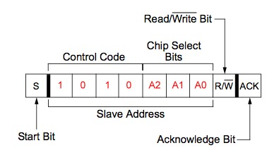
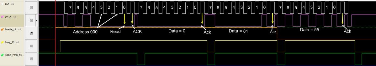
  In I2C communication we get an acknowledgment bit after each byte.   Acknowledgment bits are not supported by the SPI communication protocol.
  I2C ensures that data sent is received by the slave device.   SPI does not verify that data was received correctly.
  I2C is an address base bus protocol, you have to send the address of the slave for the communication.   In case of the SPI, you have to select the slave using the slave select pin for the communication.
  I2C has some extra overhead due to start and stop bits.   SPI does not have start and stop bits.
  I2C supports multiple devices on the same bus without any additional select lines (works on the basis of device address).   SPI requires additional signals (slave select lines) lines to manage multiple devices on the same bus.
  I2C is better for long distances.   SPI is better for the short distances.

I2C is minimally a 2 wire interface:-
    
    I2C Diagram
         
To begin communication the I2C Master device issues a start condition. This condition informs all the slave devices to listen on the serial data line for instructions. The I2C Master device sends the address of the target slave device and a read/write flag. Only the Slave device with the matching address responds with an acknowledgement signal. This is a major difference from the SPI interface which has slaves addressed in hardware.       

Communication proceeds between the Master and the Slave on a single line bidirectional data bus. Both the master and slave can receive or transmit data depending on whether the communication is a read or write. The transmitter sends 8-bits of data to the receiver which replies with a 1-bit acknowledgement. When the communication is complete, the I2C master issues a stop condition indicating that everything is done.   As for SPI devices the actual format of the information exchange is determined in software. Data can be 8, 16 ,32...bits wide. You must carefully examine the device datasheet to setup the connection.  Unlike the SPI format , data is read in the center of the high clock pulse not on the edges.  

When the I2C master wishes to talk to a slave it begins by issuing a start sequence on the I2C bus. A start sequence is one of two special sequences defined for the I2C bus, the other being the stop sequence. The start sequence and stop sequence are special in that these are the only places where the SDA (data line) is allowed to change while the SCL (clock line) is high. When data is being transferred, SDA must remain stable and not change whilst SCL is high. The start and stop sequences mark the beginning and end of a transaction with the slave device.
Here is a picture:-
  
        Start_Stop

Data is transferred in sequences of 8 bits. The bits are placed on the SDA line starting with the MSB (Most Significant Bit). The SCL line is then pulsed high, then low. The data line is an Open Collector pulled high by an external resistor,  so a high is essentially a  "lets go" control. The resistor actually pulls the line high. The receiving device (if active),  sends back an acknowledge bit, so there are actually 9 SCL clock pulses to transfer each 8 bit byte of data. The receiving device sends back a low ACK bit, indicating to the master it has received the data and is ready to accept another byte. If the data line is high at this point,  then it is an indicating of a problem and the master will terminate the transfer by sending a stop sequence. 

Because of the Open Collector format,  line lengths tend to be short and speeds are typically up to only 100KHz. Although these days much higher speeds are sometimes seen over short lengths.  We will run our test system (see below) at 10KHz.

The first byte sent by a I2C bus master is an 7 bit address to 'wake up' an appropriate slave. Almost universally the format of the address is:-
    
    Address Byte
    
This would allow in theory up to 128 slaves.  In practice most I2C devices only use 3 bits. If there is only one I2C slave the address byte is often 1010000X. The lowest bit, bit 0 of the first byte is very important. If 0 it switches the I2C slave into read mode. If 1 it switches the I2C slave into write (back to the master), mode.

We will use as a model system a I2C interface to a AT24C512 EEPROM.  See here for a the datasheet.
     
    EEPROM Chip
  
If pins 1,2 and 3 are grounded the EEPROM will read data from an I2C bus master with an address of 000, (i.e. 10100001) and write data back to the master with an address of 10100000.
Lets look at the signals for a write of 3 bytes of data to the EEPROM. For now,  lets ignore what these 3 bytes of data mean.
Here is a logic probe display. For now just look at the CLK and DATA signals (pins 6 & 5 of the chip):-
   
    Address Byte1

The above signal address the EEPROM (with a slave address of 000H).  It writes to the EPROM at address' address 0081H a byte value of 55H.
If we wanted to read the byte back at this same address bit 0 of the first byte sent would be 1.

What we now need to do is program our FPGA to actually construct these signals.

The FPGA I2C Code.
There are numerous examples of building a FPGA I2C interface on the web.   As a beginner, frankly I found a number of them overly complex and/or confusing.   Fortunately I discovered a simple and well explained example by Scott Larson here.  In that example the I2C FPA code is in VHDL.  Fortunately the code was designed using Quartus II.  So in line with all our previous examples we simply take VHDL code and convert it to a block diagram (a .bdf file).    To recap, we do this by loading up the VHDL text file my_I2C_master.vhd,  and from the file menu drop down to Create/Update, Create a symbol file. The new symbol file module will then be in the Project dropdown menu.
Here is the core of the
my_I2C_master.bdf module:-  
   
    my_i2c_master

Unlike the situation with an SPI interface for I2C we cannot simply bang out 8 byte chunks of data serially. As explained above the first byte of data to any I2C device must contain its "wake-up" address. The number of following bytes can vary a lot -- depending on the device.  Here are a few examples of the format for our EEPROM.
    
       EEPROM Format
   
From the above it's clear that the will be a minimum of two bytes for any transmission. In most cases more.  We can take care of the first byte easily because it is always the same (only the R/W bit changes). However we need to have the ability to add a variable number of bytes for the second and later bytes.  We need to 'feed" the bytes to the DATA_TO_I2C_BUS continuously as needed and as shown in the above format.  One way to do this is to use a FIFO (First In First Out RAM buffer),  which is synchronized for each byte with the  my_I2C_Module's busy flag.  For EEPROM writes: each time the busy flag goes low indicating the previous data has been sent, it clocks the FIFO to send the next byte.   When all the data has been sent, there is a flag on the FIFO that goes true when it is empty. This flag is then used to terminate the my_I2C_master transmission. For EEPROM reads life is a little simpler. We still need to send the required i2C slave address,  but we can read any number of returned data bytes as they come back as long as the my_I2C_master busy signal is high.  Here is the circuit for the FIFO:
      
    FIFO Schematic
   
As for I2C modules, there are a multitude of examples of FIFO code on the web. I found this article and code by Faraz Khan to be excellent and easy to implement.

One small modification had to me made to Scott Larson's I2C_master code.  We need a pulse (LOAD_FIFO) after the first byte has been sent -- as well as all subsequent bytes. His busy signal does not do this. This extra output is in the my_I2C_module.  This is shown in the Signal Analyses picture above  "LOAD_FIFO_T4".  Also keep in mind it is essential that my_I2C_master ena signal stays high all the time while data is being sent or read out from the module. We do this by simple latches.  Here is the circuit for the write signal.
 
       Reset ENA
   
Please download, open and study the Quartus I2C.Zip
.brd files.

The actual hardware addition to the board is just the addition of the EEPROM.  Since the two I2C lines of these EEPROM's work with a 3.3v interface we avoid the 74LVC245 voltage level shifters and connect the pins direct to the FPGA via the P11 socket. (Take care these pins never see 5 volts).  Strictly for logic probe analysis,  we will bring out certain signals from the FPGA to jumpers on P65.   Jumper K3 2-3 for a chip ID address of 00H. Jumper P37 1-2 and 3-4 to hookup the FPGA_R12 & FPGA_R13 lines. 
Here is the schematic.
     
     PROM_Schematic 
   

Also bits 0-3 of the LED bar will show bits 0-3 of the current address of the FIFO. This is useful for debugging. On power-up they should be off (i.e. address 0H).
Also we have:-

LED_4 = FIFO Full
LED_5 = I2C Error
LED_6 = FIFO Empty
LED_7 = FIFO Busy


Here is a picture of the board under test.
This circuit is one of the components of the FPGA Board Shield #1 board.
   
       
     EEPROM_Board
    
Before we jump into software,  lets run a very simple diagnostic test on the chip/interface.
To write 33H to the EEPROM at 0001H we would send from our Z80 monitor:-

QO 68,01        ;Low address
QO 68,00        ;High Address
QO 68,33        ;Data to be written
QO 69,00        ;Activate FIFO
QO 6A,00        ;Activate my_I2C_master

With the above,  a byte is written to the EEPROM at 001H.  Please note, because of the circuit layout you must always pulse the 69H port (the actual data does not matter) before activating the I2C FPGA module. This is done by pulsing the 6BH port. Again the actual data sent does not matter.

Reading the I2C is a little different.  Internally there is a "pointer" within the chip that remembers the last RAM location. So to read a byte at any location we must set up this pointer first.
We reset it back to 001H with

QO 68,01        ;Low address
QO 68,00        ;High address
QO 69,00        ;Activate FIFO
QO 6B,00        ;Activate my_I2C_master

As you can see its the same as a byte write,  except no data is sent. 
We now have the EEPROM pointer set to point to 001H so to read the data we send:

QI 6B                   ;This pulses/activates the my_I2C_master to read the I2C data line. (The monitor actually displays 11111111, which we ignore).
QI 68 00110011  ;This is the actual EEPROM data stored in the FPGA buffer and from the EPROM at address 0001H.

If you do not get the above results check your board/layout before going further.

A I2C Test Program
To really test and demonstrate the I2C/FPGA setup describe above I wrote a simple test program to run at 100H with your Z80 CPU.
All the build files are supplied below.  To recap, you assemble the program on your PC in a "Altair" Z80 simulator as described here.
You transfer the I2C.com file (also supplied below), to your S100 bus system with the Z80 Master monitor "X" command over your serial/modem connection. 
Place the file to 100H in RAM.
When downloaded, jump to 100H in RAM with the G command.

The menu more or less says it all. Here it is:-
     
    Test Program 
 
One thing strange about these I2C EEPROMs; While you can read or write multiple bytes (from a starting address), you can only do so for up to a "page" at a time. 
A page here is 80H bytes. Also as best I can tell to get a full page processed you can only do so on a page boundary. 
Of course if you do a single byte (with its own addressing), you can access any location for that data.

The #4 & #5 menu items show the utility of our S100 bus FPGA board.  These menu items allow you to move a page of S100 bus RAM to the EEPROM or vice versa.
Please take time to check out the Z80 code.  A nice addition would be to enlarge upon the above program and allow one to upload a classical Intel HEX file to the EEPROM. All 512 bytes. Perhaps one of our users could step up to the task.


BUGS
No bugs reported at this time. 

AT24C512 (IC2 EEPROM).pdf                    (V1.0 12/18/2018)
my_i2c_master.vhd                                            (V1.0 12/18/2018)
I2C_FIFO.V                                                              (V1.0 12/18/2018)
Quartus I2C Folder.ZIP                                   (V1.0 2/23/2018)

Z80_TEST.Z80            
                                  (V1.0 2/23/2018)
I2C_Z80_TEST_PROGRAM.ZIP           (V1.0 2/23/2018)


Other pages describing my S-100 hardware and software.
Please click here to continue...

This page was last modified on 07/31/2019