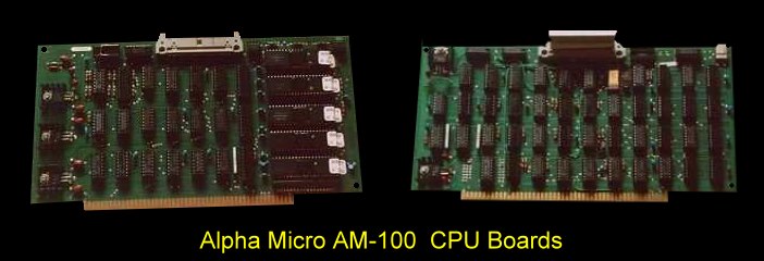
It was a dual board set with a 40 conductor ribbon connector over the top
connecting the two boards together.
The CPU was the
Western Digital WD16 40 pin MOS/LSI microprocessor chipset. This was essentialy
a copy of the LSI PDP-11 chip set. There were five
of them as seen above in the first board shown. There chips consisted of:-
DATA CHIP. The data chip provided the interfacing capability for data
and addressing. A 16-bit Data and Address bus (DAL) interfaced the CPU to
external logic. It also contained eight l6-bit registers, the Arithmetic
Logic Unit (ALU), microinstruction bus lines, and some microinstruction
decoding logic.
CONTROL CHIP. The control chip contained the microinstruction address
register which controlled accessing of the microinstructions. It also
contained translation array logic and the interrupt logic. The master timing
control was directed by the control chip which indicated when an address was
valid on the data address lines and indicated a read or write operation and
a byte or word operation.
MICROM CHIPS (3). The microm chips were 512 word by 22 bit ROMs which were
programmed to Alpha Micro specifications. These 22-bit outputs comprised the
microinstruction bus (MIB) that allowed the chips in the CPU to communicate
with each other (MIB00-MIB21). Each ROM location contained a l6-bit
microinstruction, two control bits, and four auxiliary bits. The l6-bit
microinstructions and the two control bits form a high impedance tri-state
bus. Bits MIB18-MIB2l were the auxiliary bits and were the state codes that
directed external logic to perform special functions.
MICROINSTRUCTION BUS. The Microinstruction Bus (MIB) was a high
impedance MOS bus for data transmission between the chips in the CPU and was
very sensitive to external monitoring even with oscilloscope probes.
The capacitors located on CPU 1 suppressed noise and optimize data
transmission on the bus. Bits MIB00-MIB10 served a dual purpose,
During the portion of the cycle that addresses the microinstruction from the
microm, these bits contain the 11-bit address. During another part of the
cycle, they are used to transmit the microinstruction to the other chips.
Bits MIB11-MIB17 just transferred part of the microinstruction. Therefore,
during the address phase, MIB00-MIB10 addressed the microinstruction and
during another phase MIB00-MIB17 transferred the microinstruction.
The board utilized a 4MHZ crystal divided by to to give a 2MHZ CPU clock and
Clock 1 & 2 on the S-100 bus. The chips themselves used a 4 phase
clock signal. The CPU set could recognize 4 hardware interrupts.
Where it "wandered" from the S-100 bus was that it had 7 levels of DMA
capability utilizing unused S-100 lines for signals. Since some of these
lines were critical for 16-bit transfers with the IEEE-696 specifications
this CPU board would not work with later S-100 systems. Indeed while
Alpha Micro first supplied the system in an IMSAI box the front panel
switches did nothing. Later of course they had their own box.
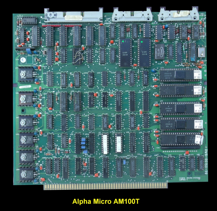
Later on Alpha Micro combined both boards into one double height board
called the AM100T.
They also added new 2 serial ports and another port for the status
display.

Alpha micro had numerous systems over the years. Most were not in fact S-100
systems.
One place where Alpha Micro really excelled was with their documentation.
Even today an extensive web site of documentation exists and can be obtained
here.
The excellent and detailed manual for this board can be obtained
here.
A description of the WD16 Instruction Op-codes can be obtained
here.
Hank Kee back in Aug 1981 wrote a brief review of the system for
Microsystems (Vol 2, #4, p 26). It can be obtained
here.


