

| Home | S-100 Boards | History | New Boards | Software | Boards For Sale |
| Forum | Other Web Sites | News | Index |
 |
I/O Port Addressing
The I/O port decoding
circuitry is comprised of two 22V10 GALS (U1 & U2) and six 74LS682N 8
bit magnitude comparators. This combination of IC’s provides independent
8 bit and 16 bit port addresses across all three board functions giving
better control over I/O port resource allocation.
The 74LS682N 8 bit magnitude
comparator circuit should be familiar territory for most of us,
essentially this IC compares two binary 8 bit words fed into two 8 bit
ports, if the data on both 8 bit ports match then the output pin 19 will
go active LOW to signify a match, in all other cases pin 19 will be
high.
We can see from the diagram
extract below (fig 1) that a subset of the buffered CPU address lines
are connected to one 8 bit port (P0 -> P7) and the second 8 bit port is
connected to a 8 way DIL switch permitting the user to specify the I/O
address to match. The 74LS682 that decodes the 16 bit address space has
an extra 3 pin header that permits the selection of one of two
Pre programmed upper 8 bit
addresses (bA8 -> bA15) 02xxH or 03xxH this allows standard IBM PC I/O
port addresses to be configured.
Now as it stands the
magnitude comparator outputs will pulse low every time the connected
address lines match the DIL switch settings regardless of whether the
CPU is generating a memory access or I/O port access, therefore further
qualification of the pin 19 outputs are required using the S100 bus
control signals.
It should also be noted as
you review the 3 groupings of 74LS682’s that some port inputs are not
used and connected to GND, in these cases the corresponding DIL switch
will always be in the ‘ON’ position for correct operation. These same
switches also provide a convenient way to disable a particular board
function (OPL3/Game/Serial) if required by placing the switch in an open
position
Starting with the first
equation in U2
P_03xxH = /A15 *
/A14 * /A13 * /A12 * /A11 * /A10 * A9 * A8
The
above two equations produce two
outputs on pins 18 & 19 corresponding to 03xxH and 02xxH, these outputs
are then wired to the 3 pin headers K2,K3,K4 (shown in fig1) satisfying
the upper byte requirement of a 16 bit address space.
The magnitude comparator
outputs from all six 74LS682’s are then passed into pins 6,7,8,9,10 & 11
of GAL U2 as unqualified decoded 8 and 16 bit addresses for the 3 board
functions (OPL3/Game/Serial).
Remember, at this stage the
pin 19 outputs will go active low on any address line match whether it
is an I/O or memory cycle.
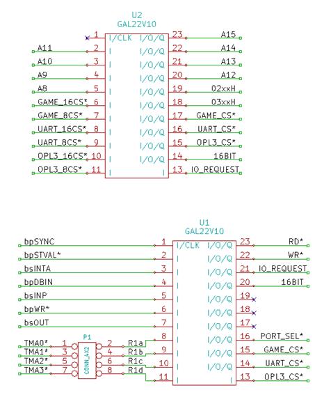 |
The next three equations in
GAL U2 complete the decoding of the Chip Select lines by ‘ANDing’ the
unqualified decoded 8 & 16 bit address’s with
IO_REQUEST and
16BIT, these inputs are generated by GAL U1 and enter
GAL U2 as inputs on pins 13 & 14.
Note how each Chip Select equation has two expressions, one line for 16 bit and the other line for 8bit decoding. The active line is determined by the logical state of the 16BIT status input.
/GAME_CS =
/GAME_16CS * 16BIT * IO_REQUEST
/UART_CS =
/UART_16CS
* 16BIT * IO_REQUEST
/OPL3_CS =
/OPL3_16CS
* 16BIT * IO_REQUEST
T
he fully I/O decoded Chip Select lines are finally output on GAL U2 pins 15, 16 & 17
IO_REQUEST = sINP + sOUT
The first equation generates
the I/O request signal using the S100 bus signals sINP and sOUT to
identify a I/O port bus cycle, this signal is output on pin 21 passed to
GAL U2 pin 13
/16BIT = TMA0 * TMA1 * TMA2 * TMA3
The 16 bit port address status signal is generated by
‘NANDing’ all 4 TMA lines together, if any one of the TMA lines go LOW
then the output will go HIGH indicating a 16 bit CPU board is active.
So referring to (fig 2) we
add a jumper to each TMA location that would be pulled low by a 16bit
CPU board thus enabling GAL U1 to distinguish between 8 bit and 16 bit
port address requirement.
The 16BIT signal is output on
pin 20 and passed to GAL U2 pin 14.
/RD = pDBIN *
sINP
The Read and Write control
signals are again generated from S100 bus signals and are used to
control/indicate data direction. Used by the on board devices and the
data bus buffers.
PORT_SEL = OPL3_CS * UART_CS *
GAME_CS
Finally, the
PORT_SEL status signal is generated from the fully decoded Chip Select
signals. If any one of the three Chip Select signal goes active LOW then
the PORT_SEL signal will
also go low allowing data to pass over the data bus buffers.
The PORT_SEL signal is output on pin 16 and connects to U8 pin 2 & 4
Game Port Circuit
Moving on to the first of the
three board functions the core of the game or joystick port circuit is a
direct implementation of the circuit published in the IBM technical
reference manual for the PC XT.
This circuit changed very
little over the early development of the PC with the NE558 clearly seen
on many PC ISA bus soundcards of the era before this circuit
functionality was moved inside of sound card ASICs.
Circuit operation is actually
very simple, the NE558 contains 4 timers whose output pulse width is
determined by the time constant of a capacitor (C11, C12, C18 & C21) and
variable resistor (Joystick) in series with a fixed resistor (R3, R4, R5
& R6). The fixed resistors set the minimum pulse width of the timer to
ensure that the pulse is measureable under software.
The output pulse (high) begins with the triggering of the timer inputs on pins 3,6,11 & 14 by performing a write operation to the game I/O port (the actual value written is irrelevant as it is not used). Following this write operation the Game I/O port is now read by software polling method to determine the width or length of time each channel takes to return to zero. The values obtained are used to determine the X-Y axis position of the two joystick units. Provision has also been made to poll the status of two buttons per joystick using the spare 4 bits available on the I/O port.
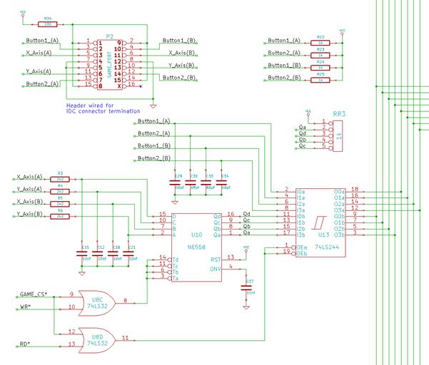 |
Finally, U8C and U8D provide
the necessary read/write steering to trigger the NE558 timers on an I/O
write cycle and enable the octal buffer (74LS244) on a read I/O cycle to
enable the joystick data to be read.
Serial Port Circuit
For a starting point I have
included some Z80 code (separate file) for an X-modem routine, the code
was brought together from various sources, credits given in the listing
header.
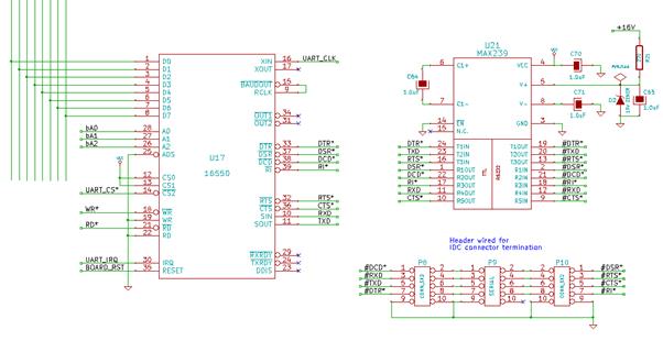
The MAX239 (U21) provides TTL to RS232 level shifting duties for the PC16550, the full complement of serial port signals are made available on output header P9 (via patching headers P8 & P10) wired according to the standard male DE-9 serial plug specification.
It goes without saying that this
configuration was chosen to provide an extra PC compliant serial port
under MS-DOS on the S100 bus.
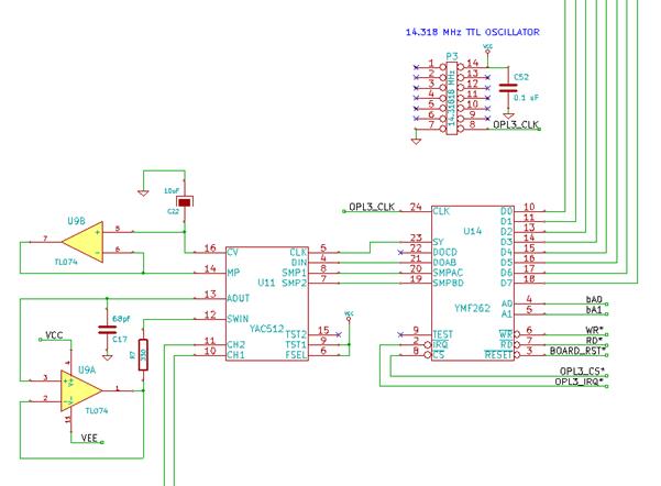
OPL3 Adlib Sound
(Digital)
The digital section of the
OPL3 sound circuit is stock datasheet implementation.
Examining an ISA sound card I
had to hand and comparing to the YMF262/YAC512 datasheets this would
seem to be standard practice.
 |
Points of note:-
OPL3 Adlib Sound (Analog)
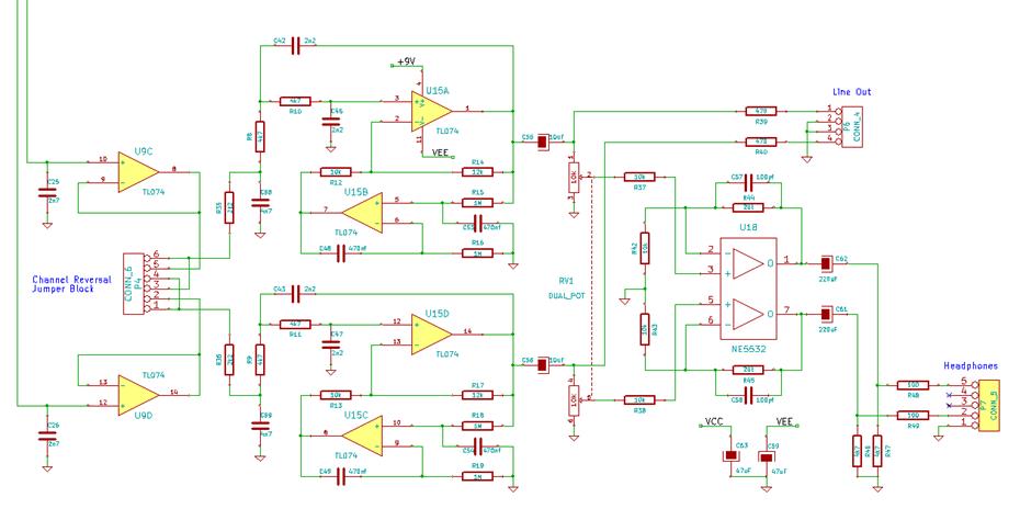 |
It is divided into 3 distinct
sections, sample & hold buffer, low pass filter, and output amplifier.
Sample
and Hold Buffer
Referring back to the previous
section we mentioned that the L + R outputs of the DAC (YAC512M) are sample
and hold switches, this means that each output channel presents the analog
sample voltage for slightly less than 50% of the time. Use of a holding
capacitor followed by a buffer op-amp allows the circuit to maintain or
‘hold’ this sample voltage until the next analog sample voltage is
presented. In order to prevent this voltage leaking away between samples a
low input current FET audio op-amp is used to buffer the signal and drive
the low pass filter.
During my initial research for
this card I tried to determine which DAC channel (A or B) corresponded to
left or right, it turns out that some sound card manufacturers
wire it one way and some the other.
Clearly one way is correct and the other wrong so I added in a patch block
to allow the end user to determine for their self.
Low
Pass Filter
The low pass filter circuit
serves to remove any sampling noise products and to this end has a
18db/octave slope with cut off frequency around 15khz (FM radio quality),
this combined with the YMF262 sample rate of 49.7khz places the sampling
noise components some 60dB below the audio signal.
The 18dB/octave filter slope is
formed first by a 6dB/octave passive filter (R35 + C68) and this is followed
by a 12dB/octave active filter centered around op-amp U15A which is
configured for a gain of 2.2 (6.8dB).
One of the obstacles that need to
be dealt with is the removal of the DC component in the audio signal as the
YAC512 DAC biases the output audio signal on a DC voltage of ½ VCC (center
point). Since we also now have some gain in the low pass filter if we did
nothing then the audio signal output of the low pass filter would now be sat
on a DC level of 5.5v. The original OPL2 Adlib card used a bit of a kludge
to deal with this situation using a transistor to remove the charge across a
DC blocking capacitor. I have adopted a different approach by incorporating
a DC servo (U15B) in the low pass filter feedback loop and this effectively
removes the DC component of the filtered audio signal by raising the DC
input voltage on the inverting input of U15A. In essence the two op-amps
work in tandem each having its feedback loop closed by the other device but
in different frequency ranges to achieve the desired result.
Output Amplifier
Output amplifier duties are
handled by a NE5532 dual op-amp IC, this IC is well known in the audio
community for its good sound, good output drive capability, and low price.
The circuit is a fairly simple headphone amplifier with a fixed gain of 3
(9.5dB) which at full volume allows the output voltage to swing to approx. 7v
p-p, enough to drive a pair of high impedance headphones or at slightly
lower listening level a pair of 32 ohm in ear phones. Resistors R48 + R49
serve to prevent output current clipping (protecting the op-amp) when
driving low impedance earphones.
The board also has a fixed line
level output connector for audio connection to a pair of active speakers.
Every effort has been made to
preserve audio quality in the analog circuitry through the use of a split
rail power supply, polyester film capacitors and Nichicon FG audio grade
electrolytic capacitors. I would recommend using the parts suggested in the
BOM as the cost difference is negligible.
The above is a
brief schematic overview in explaining
the fundamental operation of the 3 main circuit functions, In the full
schematic (see below) there are various other
circuit elements. Many of these are common to
the other S100Computer.com boards and should be
familiar to most builders.
If you have any further queries
regarding a certain aspect of circuit operation then please post a question
to the S100Computers Google Groups forum and David
will try his
best to answer.
GAL Code
What follows below is the full PALASM design descriptions for the two GALs (U1 & U2) used in this project.
;PALASM Design
Description
;----------------------------------
Declaration Segment ------------
TITLE
U1 - I/O Control GAL for S100 OPL3/Game/Serial Board V1.1
PATTERN
REVISION V1.0
;-----------------------------------
Boolean Equation Segment ------
EQUATIONS
PORT_SEL = OPL3_CS * UART_CS *
GAME_CS
/16BIT = TMA0 * TMA1 * TMA2 * TMA3
/RD = pDBIN * sINP
/WR = /pWR * sOUT
IO_REQUEST = sINP + sOUT
;PALASM Design Description
;---------------------------------- PIN Declarations ---------------
PIN  1         NC                     ; Not Currently Used
PIN  2         A11                    ; (H) INPUT
PIN  3         A10                    ; (H) INPUT
PIN  4         A9                     ; (H) INPUT
PIN  5         A8                     ; (H) INPUT
PIN  6         GAME_16CS              ; (L) INPUT
PIN  7         GAME_8CS               ; (L) INPUT
PIN  8         UART_16CS              ; (L) INPUT
PIN  9         UART_8CS               ; (L) INPUT
PIN  10        OPL3_16CS              ; (L) INPUT
PIN  11        OPL3_8CS               ; (L) INPUT
PIN  13        IO_REQUEST             ; (H) INPUT
PIN  14        16BIT                  ; (H) INPUT
PIN  15        OPL3_CS                ; (L) OUTPUT
PIN  16        UART_CS                ; (L) OUTPUT
PIN  17        GAME_CS                ; (L) OUTPUT
PIN  18        P_03xxH                ; (H) OUTPUT
PIN  19        P_02xxH                ; (H) OUTPUT
PIN  20        A12                    ; (H) INPUT
PIN  21        A13                    ; (H) INPUT
PIN  22        A14                    ; (H) INPUT
PIN  23        A15                    ; (H) INPUT
EQUATIONS
P_03xxH =    /A15 * /A14 * /A13 * /A12 * /A11 * /A10 * A9 * A8
P_02xxH =    /A15 * /A14 * /A13 * /A12 * /A11 * /A10 * A9 * /A8

/GAME_CS =    /GAME_16CS * 16BIT * IO_REQUEST
            + /GAME_8CS * /16BIT * IO_REQUEST

/UART_CS =    /UART_16CS * 16BIT * IO_REQUEST
            + /UART_8CS * /16BIT * IO_REQUEST

/OPL3_CS =    /OPL3_16CS * 16BIT * IO_REQUEST
            + /OPL3_8CS * /16BIT * IO_REQUEST
CONSTRUCTION
The aim of this guide is to provide a
recommended sequence for populating and testing your S100 multimedia card in a
step by step fashion. This method
has primarily been adopted to allow the PCB to be built up whilst at the same
time leaving sufficient space around the two surface mount IC’s to allow them to
be mounted towards the end of the process.
It should be noted that whilst
building up both the prototype (V1.0), and this board (V1.1) I have had two
failures of the YAC512 DAC chip, I cannot say for sure this was due to ESD
damage but I believe that ESD precautions would be prudent to minimize any risk.
It should also be noted
that this card uses the 8v, +16v & -16v
rails on the S100 bus to power the various circuit elements
so please make sure your system satisfies these requirements before going
any further.
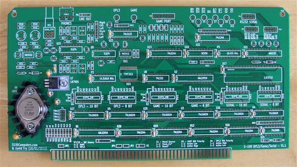
Fit the power supply components:-
0.1uF 50v MLCC Capacitor (5mm pitch)
-
C1,C4,C9,C10,C15,C16,C19,C20,C23,C24,C27,C28,C31,
C32,C35,C36,C38,C39,C40,C41,C44,C52,C60
33uF 25v Tantalum (2.5mm pitch)
- C2
10uF 25v Tantalum (2.5mm pitch)
- C3
1uF
25v Tantalum (2.5mm pitch)
- C7,C8
Can use 0.1uF MLCC if you prefer
9.1v 500mW Zener Diode
- D1
10v 500mW Zener Diode
- D2
270R Resistor (MFR3)
- R21
330R Resistor (MFR3)
- R2
LM7905 (TO220)
- U7
LM7805 (TO3) - U6
Notes:-
Both U7 and U6 need to be insulated from the PCB to avoid shorting
traces.
Mount U7 using a silicone
insulating washer and plastic insulating bush,
Mount
U6 using 2 x TO3 mica washers underneath the heat sink and 1 x silicone washer between
the heat sink and the LM7805.
 |
Check your work for solder bridges
etc.. and then plug the card into a bus extension card, using a multi-meter
check the following voltage points. Identify any faults and correct before
moving on.
D1 Cathode
+9.1v (+ – 0.5v)
D2 Cathode
+10.0v (+ – 0.5v)
U18 pin 8 (NE5532)
+5.0v (+ – 0.2v)
U18 pin 4
–5.0v (+ – 0.2v)
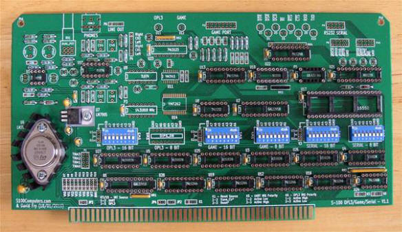
Now fit the DIL sockets, Resistors &
Switches as listed below:-
8 pin DIL Socket
- U18
14 pin DIL Socket
- U24,U8,U15
16 pin DIL Socket
- U22
20 pin DIL Socket
-
U20,U19,U12,U16,U4,U26,U3,U25,U5,U27,U13,U22
24 pin DIL Socket (0.3”) - U1,U2,U21
40 pin DIL Socket - U17
Oscillator Socket - P5
8 way DIL switches - SW3,SW1,SW4,SW2,SW5
10k Resistor SIL (5 pin bussed)
- RR1
4k7 Resistor SIL (5 pin bussed)
- RR2
1k Resistor SIL (5 pin bussed)
- RR3
4k7 Resistor SIL (10 pin bussed)
- RR5
100R Resistor
(MFR3)
- R34,R48,R49
470R Resistor
(MFR3)
- R26,R27,R39,R40
1k Resistor
(MFR3)
- R22,R23,R24,R25
2k2 Resistor
(MFR3)
- R3,R4,R5,R6,R35,R36
4k7 Resistor
(MFR3)
- R8,R9,R10,R11,R46,R47
10k Resistor
(MFR3)
-
R12,R13,R37,R38,R42,R43,R44,R45
12k Resistor
(MFR3)
- R14,R17
1M Resistor
(MFR3)
- R15,R16,R18,R19
 |
Now fit the Pin Headers & Capacitors
as listed below:-
2 x 3
0.1” Pin Header
-
(K7,K8),(K9,K10),(K11,K12),(K13,K14)
2 x 4
0.1” Pin Header
- P1
2 x 5
0.1” Pin Header
- P8,P10
1 x 3
0.1” Pin Header
- K1,K2,K3,K4,K5,K6,K15
1 x 6
0.1” Pin Header
- P4
1 x 4
RA 0.1” Pin Header
- P6
2 x 8
RA 0.1” Boxed Header
- P2
2 x 5
RA 0.1” Boxed Header
- P9
68pF 50v MLCC 2.5mm pitch
- C29,C30,C33,C34
100pf 50v MLCC
5mm pitch
- C57,C58
2n2 100v Film 5mm pitch
- C42,C43,C46,C47
4n7 100v Film 5mm pitch
- C68,C69
10nF 100v 5% Film 5mm pitch
- C11,C12,C18,C21,C37
470nF 100v Film 5mm pitch
- C48,C49,C53,C54
10uF 16v Tantalum 2.5mm pitch
- C66,C67
1uF 100v Radial Electrolytic
- C64,C65,C70,C71
10uF 50v Nichicon FG electrolytic
- C14,C6,C55,C56
47uF 63v Nichicon FG electrolytic
- C59,C63
220uF 16v Nichicon FG electrolytic
- C61,C62
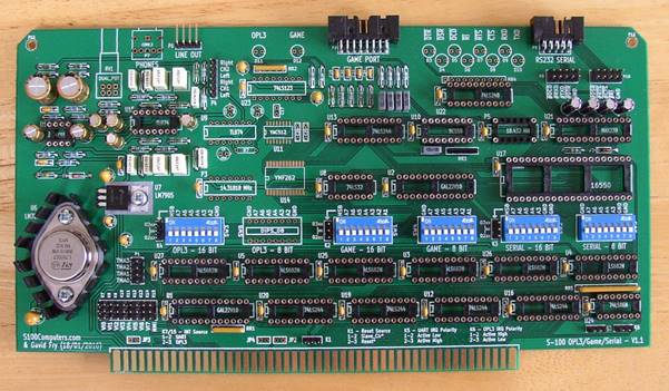
STEP 4
Now fit surface mount IC’s and
remaining
parts as listed below:-
YMF262M - U14
YAC512 - U11
Using a little PCB cleaner, clean
away solder/flux residue from U14 & U11
8 way DIL switches
- SW6
14 pin DIL Socket - U9
16 pin DIL Socket - U23
Oscillator Socket - P3
330R Resistor
(MFR3)
- R7
68pF 50v MLCC 2.5mm pitch
- C17
2n7 100v Film 5mm pitch
- C25,C26
10uF 50v Nichicon FG electrolytic
- C5,C13,C22
3mm Red LED - D3,D4,D5,D6,D7,D8,D9,D10
3mm Green LED - D11
3mm Yellow LED - D12
Using PCB cleaner, clean away
solder/flux residue from solder side of PCB then fit remaining parts:-
Stereo 3.5mm jack socket
- P7
Bourns dual 10k log pot
- RV1
10 way turned pin socket strip
- RR4

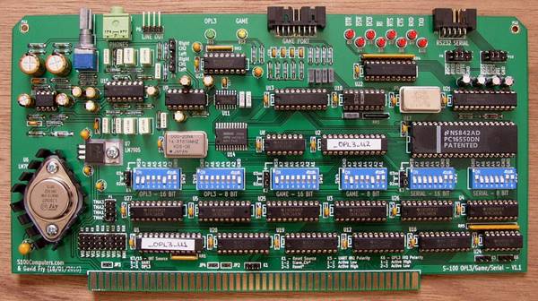
Jumper & DIL Switch Configuration
Fit all DIL IC’s and Configure
jumpers and DIL switches for use:-
Note:- The DIL switches follow the
same operating convention as other S100Computers.com boards
Audio L/R Patch
P4
1-2, 5-6
Set according to personal LR preference
RS232 Serial Patch
P8
3-4, 5-6
#RXD, #TXD
P10
3-4, 5-6
#RTS, #CTS
Reset Source
K1
2-3
Board reset from system reset
TMA Flags
P1
Fit jumpers to flag which TMA’s are used by 16 bit CPU’s
i.e. If
8088 on TMA0 then jumper TMA0
16 bit Adlib Sound
K4
2-3
03xxH MSB of port base address
SW3
11000100
xx88H LSB of port base address
1’s = off (open) & 0’s = on (closed)
8 bit Adlib Sound SW6
00000001
Set to disabled
16 bit Game Port
K2
1-2
02xxH MSB of port base address
SW1
10000000 xx00H
LSB of port base address
8 bit Game Port
SW4
01000100
88H port address for testing
16 bit Serial Port
K3
1-2
02xxH MSB of port base address
SW2
11111100
xxF8H LSB
of port base address
8 bit Serial Port
SW5
01111100
F8H port address for testing
Default 16
bit I/O Ports for PC Compatibles
Adlib Sound
0388H
Address/Status Port (R/W)
0389H
Data Port (W)
Game Port
0200H
(R/W)
Serial
COM 1
03F8H
Serial
COM 2
02F8H
Final
testing of the board is accomplished by running three small applications.
The OPL3/Adlib sound function can be
tested with the MSDOS application named DEMOFM.EXE,
The Game Port is tested with the Z80
CP/M application GAMEPORT.COM, and the Serial Port is tested with another Z80
CP/M application named XMODEM16.COM.
The DEMOFM.EXE application was found
on the internet, I can’t remember the source now otherwise I’d give credit. The
two Z80 CP/M applications GAMEPORT.COM & XMODEM16.COM
I put together using code segments
from three main sources, S100Computers.com, National Semiconductor application
note AN491 and some code I wrote myself to glue it all together.
For those who may be inclined the
XMODEM16.COM program could be developed further to make it bidirectional,
as it stands it does a good enough job of transferring files from a PC
host onto the S100 computer. The code is extensively documented so it should be
easy to follow.
Checking the OPL3/Adlib Sound
First you will need to transfer the
DEMOFM.EXE program onto your MSDOS compact flash card, or as I do, copy it to a
floppy disk if your S100 computer has a floppy disk controller (S100 ZFDC card).
Set the sound card volume control to
minimum and insert your headphone jack plug into the headphone jack socket. Turn
the volume pot to mid position, the audio output should be quiet with maybe a
little amount of low level hiss if your
headphones are particularly sensitive.
Now boot your S100 computer into
MSDOS and locate the file DEMOFM.EXE which you have transferred to CF media or
floppy. From the MSDOS command prompt launch DEMOFM.EXE with the following
command:-
DEMOFM.EXE 388H
If all is well then you should hear a
short audio jingle through the headphones and the OPL3 LED on the PCB should be
flashing to indicate that port 388H is being accessed. If you have no audio and
the LED doesn’t flash then go back and check the Jumper & DIP switch settings,
don’t forget that a jumper is needed on the corresponding TMA line to enable 16
bit port addressing.
If the OPL3 LED flashes but you have
no audio then you will need to start tracing through the audio stages with an
oscilloscope working from the DAC forwards.
Checking the Game Port
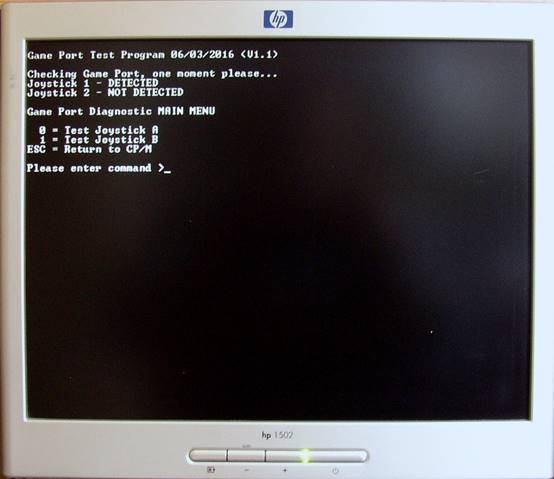 |
The game port test program
GAMEPORT.COM has been written for the Z80 CP/M 3.0 platform and uses BDOS
function calls for all console input and output allowing the program to be used
with different console I/O hardware configurations,
The first step is to transfer the
programs GAMEPORT.COM and XMODEM16.COM to your Z80 CP/M CF media card, this can
be done using the disk image utility cpmtools. The process of how to do this has
been discussed on the S100Computers Google forum before but if you are unsure of
the process then please post a question and I’ll do my best to answer.
On launching GAMEPORT.COM you will be
presented with the above screen, the program detects what if any joysticks are
connected to the port and reports accordingly. The option menu is a simple test
‘A’ or ‘B’ or exit affair. Upon selecting option 0 a line of data for X axis, Y
axis, & button status will be displayed, this line may flicker as the data is
repeatedly updated and the game LED on the PCB should also be flashing. Moving
the joystick through x axis and y axis movements should result in the binary
values increasing or decreasing, likewise pressing a joystick button should be
confirmed with the appropriate button status message.
Once you are done then pressing ESC
will return you to the menu options and from there ESC will terminate the
program and return to a CP/M prompt.
Checking the Serial Port
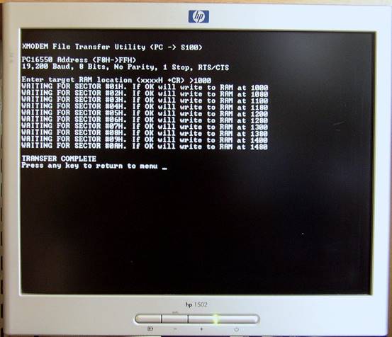 |
(you will need to fabricate a custom
cable for this) and launch the test program XMODEM16.COM
A simple two option menu will be
displayed from which you select option ‘0’ to ‘Receive a file via XMODEM’ the
above screen will be displayed.
Configure your PC terminal emulation
software serial port settings for 19,200
baud, 8 data bits, no parity, 1 stop bit, and flow control to hardware
(RTS/CTS). In TeraTerm (my terminal
software of choice) these settings can be found under the
SETUP > SERIAL PORT menu.
At the PC terminal setup an Xmodem
file transfer to send a file but don’t confirm the final ‘OK’
File > Transfer >
Xmodem > Send > Browse to file
Now on the S100 computer type the
target RAM location, I would suggest 1000H as a suitable location to avoid
problems. (The XMODEM16.COM application resides at 0100H and occupies RAM up to
about 0680H)
Now press the enter key on the S100
computer (it will start waiting for the 1st sector) and click the
‘OK’ button on the PC host to initiate the file transfer. If all is well the
file should be transferred across in 128 byte sectors with a screen entry for
each block.
If you should get timeout errors
check the serial port patching block (P8 & P10) jumpers are correctly in place
and verify your serial cable wiring. If you should get checksum errors then make
sure that your terminal software is sending checksum error correction data and
not CRC or 1k.
(This setting is a radio button in
the bottom of the file browser window in TeraTerm)
If you have other issues then please
post to the S100Computer forum where I will do my best to help.
Serial Cable Notes
The 10 pin serial port header has
been wired to allow the use of an IDC (insulation displacement connectors)
connector at each end of the cable, just be careful to ensure that pin 1 at each
end cuts into the same wire and you should be done.
If you chose to use a solder bucket
style DE9 connector then you need to remember that the pin numbers are assigned
differently. Hopefully the following list should make sense.
IDC pin 1
-> DE9 pin 1
IDC pin 2
-> DE9 pin 6
IDC pin 3
-> DE9 pin 2
IDC pin 4
-> DE9 pin 7
IDC pin 5
-> DE9 pin 3
IDC pin 6
-> DE9 pin 8
IDC pin 7
-> DE9 pin 4
IDC pin 8
-> DE9 pin 9
IDC pin 9
-> DE9 pin 5
IDC pin 10 -> DE9 pin 5 (pins 9 & 10
of IDC tied off to GND)
This page was last modified on 05/20/2020