S100 Computers

HomeS-100 Boards HistoryNew BoardsSoftwareBoards For Sale
ForumOther Web SitesNewsIndex  
 
The MEGA 328 & 2560 CPU Board  
    Mega 32802560 Board (328 Config)
   
  Mega 328-2560 Board (2560 Config)

Introduction

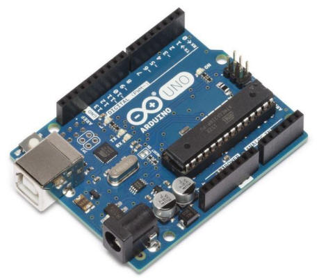
A whole world of new hobbyists have in the past decade grown up around the "Arduino" boards.  Arduino is an open source computer hardware and software (Italian) company that designs and manufactures CPU board kits for the control of objects. The project's products are distributed as open-source hardware and software. Arduino boards are available commercially in preassembled form, or as do-it-yourself kits. Arduino board designs use a variety of microprocessors. They are usually equipped with sets of digital and analog input/output (I/O) pins that may be interfaced to various expansion boards (shields) and other circuits. The microcontrollers are typically programmed using a serial communications interfaces, including (USB) on some models. Programming is often C or C++. Arduino also provides a nice integrated development environment (IDE) for writing simple "sketch" code.  Two very popular boards are the Arduino "UNO" board and "MEGA".
  
 UNO Picture  Mega Picture
 
By far the most popular "Shields" pinout is that found on the UNO.  The MEGA is somewhat similar but has more I/O pins. See here for a pinout diagram for the UNO pinout and here  for a pinout diagram of the Arduino MEGA board.

In order to use and understand this S100 bus Atmega 328/2560 CPU board you should be fairly familiar with the Arduino hardware and software.
Excellent vendors with much information about Arduino boards are "SparkFun.COM" and "Adfruit.COM" and of course Arduino itself.

Please note: this board can be driven by either the Atmega 328 or Atmega 2560 CPU chip but not both CPU's at the same time.  The first thing you have to decide is which CPU you would like the board to be setup and configured for.  Because the Atmega 2560 CPU is a surface mount chip, once it is installed on the board there is no way of going back to using the 328 CPU (without desoldering the 2560 chip from the board).  It is however possible to start with a 328/UNO configuration and later remove that chip and go to a 2568/MEGA configuration.  Because of the large number of pin connections/jumpers that would be required you cannot go back from a MEGA to UNO setup.  That said,  the UNO setup is simpler to configure, if you mainly wish to use Arduino Shields you might just stick with that setup.  For maximum flexibility you might consider building two boards.

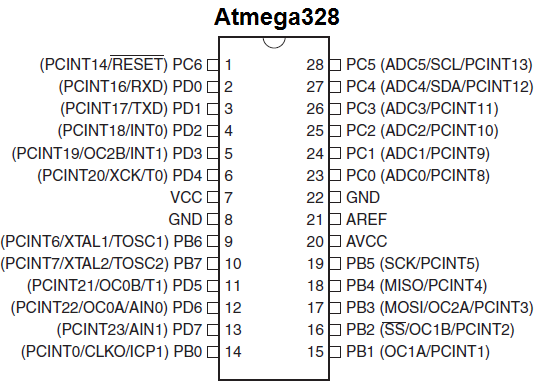
We will build a board based on the Arduino UNO board first and then later reconfigure it for the MEGA 2560 CPU as well.  This board utilizes the ATMEGA 328 CPU. The Atmega328 has 32K of flash program memory and 2K of Internal SRAM. It is a 28 pin DIP chip.  It has 14 digital I/O pins, of which 6 can be used as PWM outputs and 6 analog input pins. These I/O pins account for 20 of the pins. Here is the pinout for the Atmega328.
  
    Arduino 328 Pinout

The chip takes a 16 MHz Oscillator and runs at 3.3V or 5V, (we will use 5V).   We will work with this (simple) CPU and use it to interface I/O ports and interrupts on the S100 bus as well as interfacing with Arduino "Shields".  The trick with this few CPU I/O pins will be to have a very flexible pin jumpers arrangement.
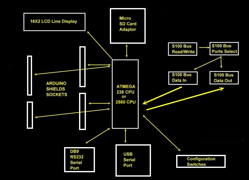
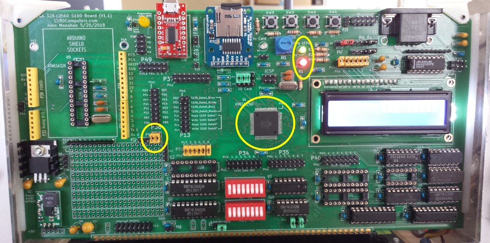
Here is a summary of the boards layout.
    
   Board Diagram
 
You can see that unlike for example our Edison CPU boards, we are not running this board in an S100 bus Master/Slave arrangement. There are simply too few available CPU pins to do so. The board will appear to the S100 bus as a set of 8 bit wide I/O ports (user defined), but is also able to trigger S100 bus interrupts.


Step By Step Building the MEGA 238/2560 CPU Board.
The build instructions are fairly simple for this board. As always, first examine the bare board carefully for scratches or damaged traces, use a magnifying glass if need be.  A broken trace is almost impossible to detect by eye on a completed board..

Build the board up in functional steps. Avoid the temptation of adding everything at once and popping it into your S-100 box. Step by step is faster in the end -- trust me.  We will set the board up as an S100 bus I/O board. 
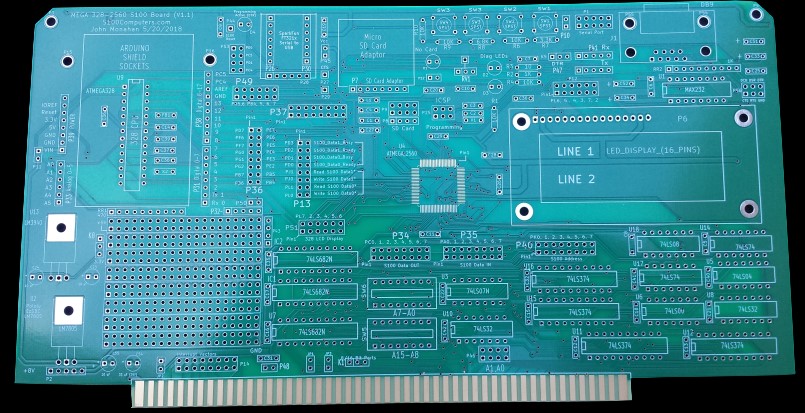
Here is a picture of the bare board:-    
  Bare Board
     
Solder in all the required IC sockets, resistors, resistor arrays, capacitors, jumpers, and the 3.3V and 5V voltage regulator.  For the latter you can use a 7805+heatsink approach (e.g... Jameco # 9246333, a L7805CV), or you can use more modern switcher regulators such as thee Pololu # 28500(5V, 2.5A) or EzSBC.com # PSU5aa(5V 2.5A). In most situations you will not need the 3.3V regulator.   Add the 10K Pot RV1 (normally supplied with the HD44780 16X2 LCD display, see below).

Do not add the LED's yet. Be sure you put the resistor arrays in with the correct orientation of pin 1. Check their values before soldering (they are difficult to remove).  Insert all jumper arrays. For prototype boards I typically use common Aluminum Electrolytic caps. For the final board I use the corresponding Tantalum caps.  There are two sockets for the RV1 (10K Pot). Use whichever best suites the actual variable Pot you get. For the DB9-RS232 socket, leave some space under it and the board so it does not interfere with the card ejector. Have it standing off just enough to solder all the pins.
   
For prototype boards I generally use "double swipe" IC sockets. For a critical board like this I prefer to use "Machine Tooled" IC sockets.  However they are more expensive and you have to be particularly careful not to bend the IC pins.     For the specialized mini boards such as the Serial to USB adaptor, the 16X2 LCD display and the Micro SD card adaptor you have a choice of directly soldering the units to the board or using a single row socket such as the
Jameco socket #308567 (cut to size). The former yields a nicer board but removal is difficult.  For prototype boards I always use sockets.

Place the board in the bus. Check the voltage to sockets on the board is about 5V by placing the board in your S-100 system using an extender board. With no load you will typically get 5.00V  (+/- 0.2V).  While not used in the construction below, check that the U13 regulator is putting out 3.3V to pin 3 of K8.  BTW, your system should boot and run correctly with its Z80 master CPU board. If not, you have a serious solder bridge somewhere on the board.  Before you do anything else with a magnifying glass go over every socket on the board and examine for proper solder joints. I like to "reheat" each joint just to be on the safe side. The silk screen/varnish on these boards us quite thick. It's easy not to have a good solder joint for the ground pins.  Double check.   Extra time here will save you hours later.  

Next insert all
4 LED's. Before soldering them in place ground the appropriate LED pin to be sure it lights up.  

One decision you need to make up-front is if you want to solder the Micro SD card adaptor, the LCD display and USB port adaptor directly to the board or use sockets. With a socket you normally will not be able to fit the board into a one board slot on the S100 bus.  While you can remove the sockets later and solder direct (I did so below for the LCD display), it requires good desoldering techniques/tools.  These adaptors seem quite reliable and robust. I recommend direct soldering.

Arduino Bootloader
If you don't already have the Arduino IDE software writing/uploading program on your PC you need to do that now.  It's best to upload it from the Arduino web site itself (https://www.arduino.cc/en/Main/Software).  Here is what it looks like:-
   
 IDE Interface

The Atmega 328 (and 2560) CPU chips as manufactured in the factory come as "virgin" chips. They must first have their onboard ROM programmed to accept an Arduino "bootloader" to allow the uploading of an actual Arduino "sketch" program.  This requires an Atmega programmer.  Fortunately the hardware & software is very standard and there are a number of cheap USB drive programmers on the web.  Personally I found the best/easiest method is to use an actual Arduino UNO board and special cable described here.  This has the advantage that it works for both the 328 and 2560 chips -- some don't.  The Arduino script file
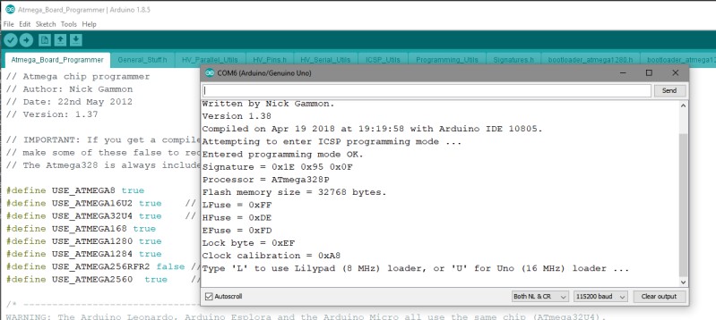
"Atmega_Board_Programmer.ino" is provided at the bottom of this page.  Follow the instructions described here, but use the Atmega_Board_Programmer.ino file provided below -- it has been edited to also allow the burning of both the 328 and 2560 CPU chips . Be sure to select 328 for the current CPU in the Arduino IDE.  Check your UNO board is recognized. You should see something like this under Tools/Board Info.:
       
    Programming IDE
 
Insert a "virgin" Atmega 328 chip in the socket marked U9 on the S100 board.
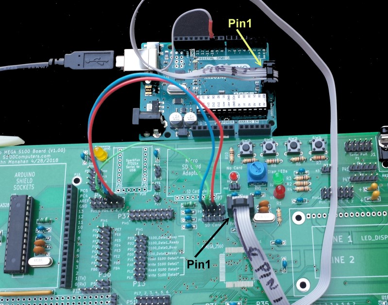
Next we need to connect up the ICSP port (P25) for programming. Make sure you position the Pin 1 of the connector/cable correctly.
Jumper P49 pin 12 to P9 pin 6, jumper P49 pin 10 to P9 pin 2 and jumper P49 pin 8 to P9 pin 4. (see the picture below).
You must have:-
   
      Arduino UNO   Target
    D10 (SS) (P25,5)   CPU_Reset
    D11 (MOSI) (P9,4 <= P25,4)  MOSI (P49, 8)
    D12 (MISO) (P9,2 <= P25,1)  MISO (P49, 10)
   D13 (SCK) (P9,6 <= P25,3)  SCK (P49,12)
  Gnd   GND
   +5V   +5V

Open the serial monitor connection in the above Arduino IDE (top RHS button).   Make sure it is set for 115200 baud.
Hookup the UNO board and S100 board as shown below. Make sure the "reset" wire #5 is connected to the UNO D10 socket.
Note the S100 board is
NOT in the S100 bus. The UNO board provides all the power that is needed.
Compile and run the above sketch file.  Here is a picture of the setup.   
      
      UNO Bootloader
    
Follow the instructions in the Arduino Serial monitor.
   
   IDE Bootloader
   
If you are new to the Arduino world you may want to start off with an ATMEGA 328 CPU already pre-programmed with the Arduino bootloader code in the chips ROM.  These are more expensive that the virgin Atmel CPU chips but can be obtained from a number of sources (e.g.. Adfruit for $5.95).   However pre-programmed 2560 CPUs (see below) are not available .

To check our uploaded is working correctly we will use it to upload a simple Arduino Sketch test file
BLINK_328.UNO using the boards USB port.  However first we need to activate a USB port on the board so we can pass software to the 328 CPU over this port (pins 2 & 3 of the CPU).

The  SERIAL to USB Adaptor   
There are numerous "chips" available for this function. We will use the Sparkfun unit.  Its simple to use and the Arduino software works directly with it. If you wish to have the unit removable,  you need to solder in 6 pin female single row socket in P28 and a corresponding male row of pins (supplied by Sparkfun) to the back bottom of the unit.  There is no need to  insert sockets in P26 or P30. They don't quite exactly line up with the unit (and are unused) anyway.
 
USB Adaptor
  
Alternatively just solder the unit to the board's P28 pins with the Sparkfun male socket pins provided as shown below.

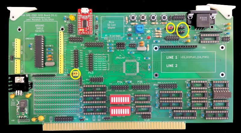
Insert U5.  Jumper
P41, 4-5,  P47, 4-5 and K5, 2-3.
Jumper P32,4 to P50,1 and P32,5 to P50,2  to connect up the two LEDs D2 and D3 to pins 5 and 6 of the 328 CPU.
  
  Step 1
    
Insert the board into your S100 chassis and power it on.
Hook a USB cable from the SparkFun FT231x to your PC's USB port. Within the Arduino IDE "
Tools Menu", assign the USB port to the Arduino IDE program and set the Arduino board type to UNO.

Copy the
ArduinoFiles.zip file at the bottom of this page across to a directory for access with your Arduino IDE. Extract all the .UNO files into a "Arduino S100 Programs" folder and load BLINK_328.INO directly from the Arduino IDE.  Compile and upload this "sketch" program.  Please note the compile process is actually fairly slow for the first time a sketch file is loaded (~1 minute).  During the upload the LED's on the FT231x board should flash.  Also the D4 LED should light up.  If this does not happen you probably either have an invalid boot loader or a bad USB port connection.  If you have a Genuine Arduino UNO board get that board working first.

If the
BLINK_328.INO program worked the LEDs D3 (RED)  & D2 (GREEN) should blink.  If not you can check your software/hardware with a genuine Arduino UNO board. Upload the BLINK_328.INO program to that unit and check that the boards shields "Pins 2 & 3" (CPU pins 4 & 5), pulsed high/low continuously.  You can use a resistor/LED as a probe.

This brings me to one problem I find with these Arduino Boards. Arduino provides convenient jumpers on their boards for connection to breadboards or to utilize custom plug-in "Arduino Shield" boards which plug in and sit on top of the Arduino CPU board.  By far is the most common jumper arrangement is the UNO jumpers arrangement.
  
 Shields Pinout

So for our
BLINK_328.INO,  we will connect the  LED to Shield pin 3.  This pin is designated as "3" in the Arduino software library. It is actually connected to pin 5 on the 328 CPU chip.  The library pin names for the UNO board is shown above.  Unfortunately (for reasons that are not clear to me), the pin arrangement and library names are not the same or a sub-set of the larger array of pins available for the Arduino MEGA 2568 CPU board.  The MEGA 2568 board as we shall see have a different pin/library arrangement.  That said, anything you can do/program on the UNO can easily be reassigned/programmed for the MEGA board.   

This does however complicate our board layout.  I have retained the "lowest common denominator", the  UNO board pin layout for the UNO shields sockets but added jumpers so that essentially any MEGA CPU pin can be utilized to drive them. While the actual shields sockets retain the UNO configuration/spacing pin designations, the schematic refers to the Arduino MEGA 2560 pin names.  This actually sounds more complicated than it is.  If you make a printout of this
328 and 2568 pinout sheet you should not have a problem.  In all your sketch programs use the "IDE" names but jumper the sockets based on the "real" CPU pin numbers.
 
You must get the above
BLINK_328.INO program working before going further.

LCD Display using the 328 CPU
Next we will get the 16X2 line LCD display working.  This fairly common display can be obtained for example from Adfruit for $10.  While others are available, this
HD44780 16X2 LCD display already has an Arduino library written to interact with it and so is easy to get going immediately.

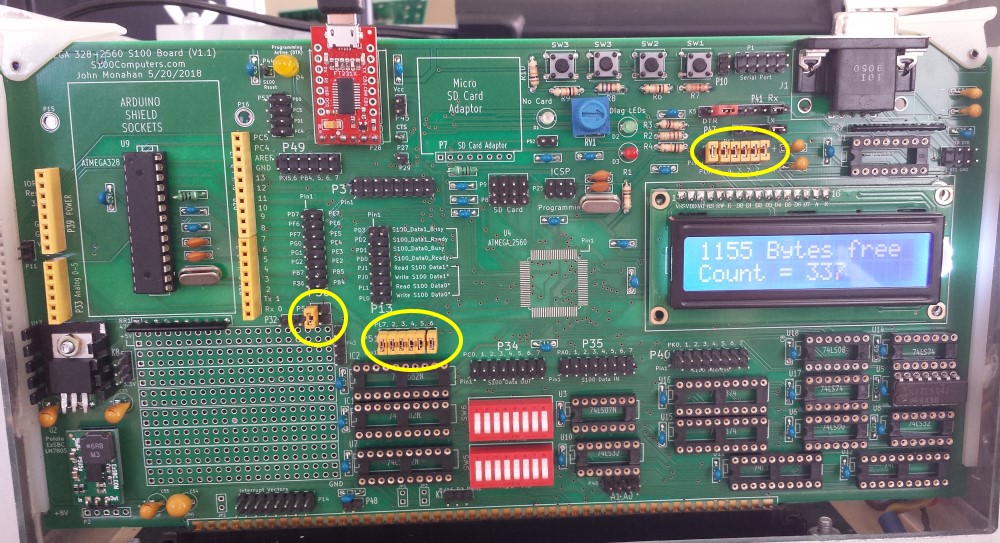
Remove P50,2          
Insert the display in its P6 socket. Again you can solder it directly or use a socket.  I like to also use two bolts for stability when using a socket.

For our 328 CPU we will drive the display with the CPU pins
14,15,6,11,12 & 13 (PB0,PB1, PD4-PB7). This corresponds to library pins 8, 9, 7, 6, 5 & 4.
So jumper P51, 1-2, 3-4, 5-6, 7-8, 9-10 & 11-12 and to the LCD display P12 1-2, 3-4, 5-6, 7-8, 9-10 & 11-12.
Compile and upload the
LCD1_328.INO file:-

#include <LiquidCrystal.h>
#include <EEPROM.h>
#include <SD.h>
#include <SPI.h>                                // required for Arduino >= 1.5.4

LiquidCrystal lcd(8, 9, 7, 6, 5, 4);            // CPU pins 14, 15, 6, 11, 12, 13 (PB0, PB1, PD7, PD6, PD5, PD4 of CPU)
                                                // PB0, PB1, PH4, PH3, PE3, PG5 on schematic
int x = 0;
                                                // the setup function runs on reset or power up
void setup() {                                  // initialize digital pin LED_BUILTIN as an output.
   pinMode(S100_WRITE, OUTPUT);
   pinMode(S100_READ, OUTPUT);                  // set up the LCD's number of columns and rows:

   lcd.begin(16,2);
   lcd.clear();
   lcd.print("LCD Initilized.");
   lcd.setCursor(0,2);
   lcd.print(FreeRam(),DEC);
   lcd.print(" Bytes free");
}

void loop() {                                   // the loop function runs over and over again forever
   digitalWrite(S100_WRITE, HIGH);
   delay(400);
   digitalWrite(S100_WRITE, LOW);
   delay(400);

   lcd.clear();
   lcd.setCursor(0,0);
   lcd.print(FreeRam(),DEC);
   lcd.print(" Bytes free");
   lcd.setCursor(0,1);
   lcd.print("Count = ");
   lcd.print(x++,DEC);
}

We will use this LCD display to issue diagnostic information about the board to us as we progress further.
Here is a picture of the board at this stage:-
       
  Setp 2
     
SD Card Interface using the 328 CPU
Next we will add the Micro SD card adaptor. This is where Arduino really shines, the complex process of writing code to interface with a MSDOS file system using a simple 8 bit CPU is already done for us.  Also helpful,  companies Adfruit supply a Adfruit MicroSD adaptor which it has a built in 3.3V to 5V level converter so we can directly splice the unit into our board. (SD cards only run at 3.3V).  The above site also has a detailed instruction list of how to interface and use the unit.
    
 MicroSD card
   
Remember, SD cards are 'raw' storage. They're just sectors in a flash chip, there's no structure that you have to use. For the Arduino library we'll be discussing, and nearly every other SD library, the card must be formatted FAT16 or FAT32. With the Arduino SD library can use either.

First format your card on your PC, start with a FAT16 format.

Because SD cards require a lot of data transfer, they will give the best performance when connected up to the hardware SPI pins on the 328 or 2560 CPU. These hardware SPI pins are much faster than 'bit-banging' the interface code using another set of pins. For 'classic' Arduino such as the Uno those pins are digital
13 (SCK), 12 (MISO) and 11 (MOSI) in the Arduino library. (These correspond to the actual 328 CPU pins 19,18 & 17).  You will also need a fourth pin for the 'chip/slave select' (SS) line. Traditionally this is library pin 10 (CPU pin 16,but you can actually use any pin you like). For the Arduino Mega 2560 as we will see later,  the pins are different!

Insert the SD adaptor in connector P7. With this arrangement the MicroSD card is now connected to the 328 CPU pins (
19,18, 17 & 16).  
Jumper P52  to provide power to the card adaptor.
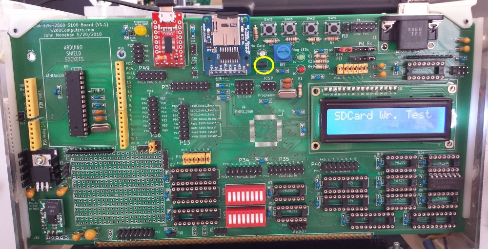
Here is a picture of the board at this stage:
    
Step 3
    
Insert a MicroSD card.  The "No Card" D1 LED should go off when you insert the actual card..

We will test our card with 3 simple sketch programs derived from the Arduino IDE "CardInfo" examples. However before we test the card we need to do one thing with the Arduino IDE.   Again launch the  handy serial terminal interface with the boards USB port.  Set its Baud rate to
115200 (bottom middle button).

Now compile and upload
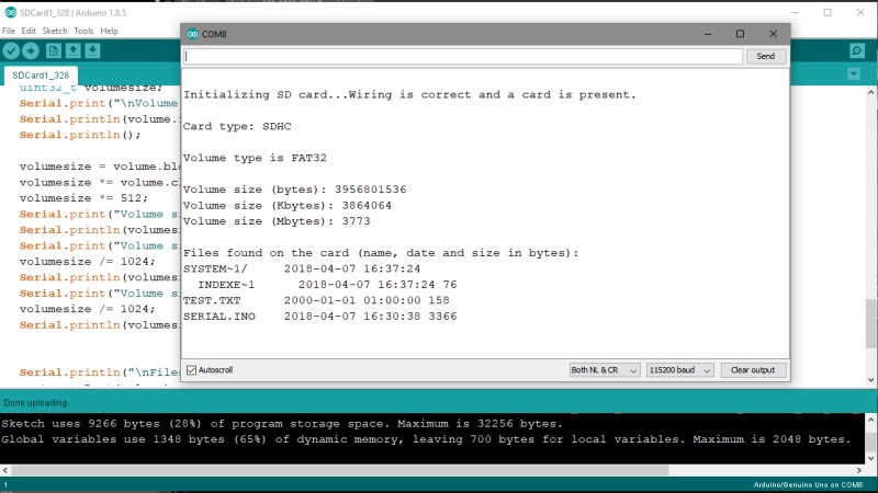
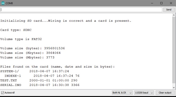
SDCardInfo_328.INO within the Arduino IDE. You should see something like this in the "Serial TTY window".  It gives you information about your MicroSD card  -- all for a few lines of code!
  
   SD Card Info
 
  
The core Sketch code is:-

Serial.print("\initializing SD card...");
pinMode(10, OUTPUT);
                                        // we'll use the initialization code from the utility libraries
                                        // since we're just testing if the card is working!
if (!card.init(SPI_HALF_SPEED, chipSelect)) {
        Serial.println("initialization failed. Things to check:");
        Serial.println("* is a card inserted?");
        Serial.println("* is your wiring correct?");
        Serial.println("* did you change the chipSelect pin to match your shield or module?");
        return;
        } else {
        Serial.println("Wiring is correct and a card is present.");
}

                                         // print the type of card
Serial.print("\nCard type: ");
switch (card.type()) {
        case SD_CARD_TYPE_SD1:
                 Serial.println("SD1");
                 break;
        case SD_CARD_TYPE_SD2:
                 Serial.println("SD2");
                 break;
        case SD_CARD_TYPE_SDHC:
                 Serial.println("SDHC");
                 break;
        default:
                 Serial.println("Unknown");
}


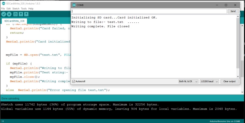
Next we will setup and write to a file TEST1.TXT some keyboard characters. Now compile and upload SDCardWrite_328.INONO. You should see something like this in the "Serial TTY window".
    
   SDCard Write
  
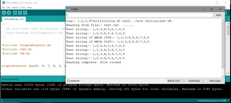
Next we will open the file TEST1.TXT and display its contents.  Now compile and upload SDCardRead_328.INO. You should see something like this in the "Serial TTY window". 
       
   SD  Card Rd
 
The core Sketch code is:-
 
myFile = SD.open("test.txt");

if (myFile) {
Serial.println("Reading from file:- test.txt ......");
while(myFile.available()){
      Serial.write(myFile.read());
      }
myFile.close();
Serial.println("Reading complete. File closed");


Please note this is a very simple example of the use of the Arduino SD library to use a MicroSD card. The SD library is quite extensive, SD Card functions are listed here.

S100 Bus IO
Utilizing the 328 CPU section of the board to read/write to an S100 bus I/O port is very limited because of the few pins available on the 328 CPU. Normally we would have to either disable the SD Card or LCD display or process only a few data bits.  (It is possible to temporally inactivate the SD card or LCD display and get the full 8 bits but I have not played around with that approach).  If you do so and develop some useful S100 bus related sketches I will be delighted to post them here.  The current board as configured is really setup to use the 328 CPU with Arduino Shields. For an S100 bus interface I will therefor illustrate only two very simple examples.

The first will be to
input a data bit from an S100 bus port that is written to port 80H by the S100 bus Z80. 
We will input and display on the LCD display (in real time) the status of
bit 0 from I/O port 80H on the S100 bus (and also on the Arduino IDE Serial interface).

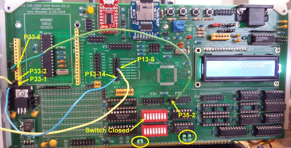
Insert the IC's U7, IC1, U6, U8, U1, U5, U18, U14, U12 & U11.
Insert the two dip switches SW5 & SW6. Set all switches to closed,  except the LHS switch of SW6.
Jumper P46 1-2, and 5-6.
Jumper K1 2-3.
Jumper P13-14 to P33-1.
Jumper P35-2 to P33-6.
Jumper P13-8 to P33-2.    
Here is a picture of the board at this stage:
  
  Stage 4
                                                                        
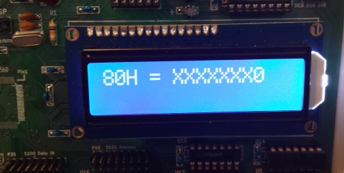
Now compile and upload S100_Port_Wr_328.ino within the Arduino IDE. You should see something like this on the LCD display.
    
   Port Write Data

Here is the relevant sketch code.

void setup() {
pinMode(READ_LED, OUTPUT);
pinMode(WRITE_LED, OUTPUT);
pinMode(READ_DATA0_READY, INPUT);
pinMode(READ_S100_DATA0, OUTPUT);
pinMode(S100_DATA_BIT0, INPUT);

lcd.clear();
lcd.print("LCD Initilized.");
lcd.setCursor(0,2);
lcd.print(" Read 80H bit 0");
delay(1000);

digitalWrite(READ_S100_DATA0, LOW);     // Clear the FF
digitalWrite(READ_S100_DATA0, HIGH);
}


void loop() {
bool x;
lcd.clear();
if (digitalRead(READ_DATA0_READY))
      {
      digitalWrite(READ_S100_DATA0, LOW);       // Activate OE* on the 74LS374
      x = digitalRead(S100_DATA_BIT0);
      digitalWrite(READ_S100_DATA0, HIGH);     
      }


digitalWrite(READ_LED, !x);
lcd.print("80H = XXXXXXX");
lcd.print(x);
delay(1000);
}

When we use the Z80 Monitor command to output to the port 80H the value of its bit 0 will be displayed.
U
se QO80,01  or QO80,FF. The (RED) D3 LED should briefly flash.

If the above did not work follow the signals with a logic probe. On the S100 bus side outputting to port 80H must pulse high pin  11 of U11. Pin 1 should pulse low with each 328 read, and pin 1 of U14 should pulse low (resetting the FF).

Next we will
output a data bit to an S100 bus port.  We will output and display a high and low value for bit 0 for I/O port 80H on the S100 bus. 
Leave the current jumpers in place.
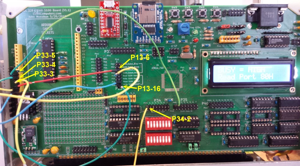
Add Jumper P13-16 to P33-5.
Add Jumper P34-2 to P33-4.
Add Jumper P13-6 to P33-3.

Here is a picture of the board at this stage
  
    
   Step 5a
   
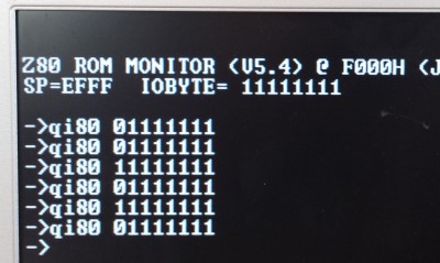
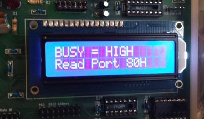
Compile and upload S100_Port_Wr_328.ino within the Arduino IDE. On your S100 Z80 Monitor you should see something like this:-
  
     328WR_a              328 WRb
 
The Arduino is flipping the bit 0 data bit of port 80h each time it is assayed by the S100 bus Z80.  Here is the relevant code

void loop() {
digitalWrite(WRITE_LED, HIGH);
   if((bool)digitalRead(S100_DATA0_BUSY))
      {
      lcd.setCursor(0,0);
      lcd.print("BUSY = HIGH ");
      lcd.setCursor(0,2);
      lcd.print("Read Port 80H ");
      }
   else
      {
      lcd.clear();
      lcd.print("BUSY = LOW ");
      if(x == HIGH)
           {
           digitalWrite(S100_DATA_BIT0, LOW);        // Latch and hold data bit
           lcd.setCursor(0,2);
           lcd.print("80H = XXXXXXX1 ");
           x = LOW;
           }
       else
           {
           digitalWrite(S100_DATA_BIT0, HIGH);       // Latch and hold data bit
           lcd.setCursor(0,2);
           lcd.print("80H = XXXXXXX0 ");
           x = HIGH;
           }
   digitalWrite(WRITE_S100_DATA0, HIGH);             // Reset the FF
   digitalWrite(WRITE_S100_DATA0, LOW);
   digitalWrite(WRITE_LED, LOW);
   delay(1000);
   }
}
 
Apologies to our more experienced programmers for the verbose code -- wanted to keep things easy for beginners.

There are definitely much more sophisticated things you can do with this 328 CPU on this board with your S100 bus system.  There is a decent size "patch area" to add your own chips. The number or available GPIO pins is however a limitation with this  CPU.  It's not as bad as you might initially think because one could multiplex 2 or 3 CPU GPIO pins with say a 74LS138 and have a workable number. Also the SD card is only active when CS* is low, and once a program is loaded it sits in the CPU EEPROM and so the USB port pins are no longer needed. 

Nevertheless the main function of this board is to use it with the 100 pin Atmel 2560  8 bit, 20MHz, CPU.  The only downside is the 2560 CPU is a surface mount chip.  Once you place it on the board there is no going back to the 328 CPU chip.   Early on I considered jumpers for the 2560 CPU to allow both CPU's.  The overall layout was way too complex and confusing.  As it is the board jumper layout is somewhat confusing!   The problem is Arduino uses different pin names on their UNO and MEGA boards.  
On this board the default pin name is for the Arduino MEGA board.  You absolutely will need to have before you the pin designations for the UNO and MEGA boards before you to get UNO programs working correctly.


The MEGA 2560 CPU Board
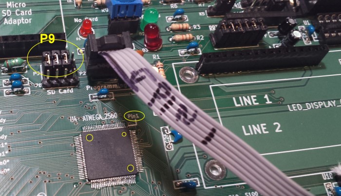
First remove the 328 CPU chip and all wire jumpers from the board.  You also might want to remove the LCD display and Micro SD card adaptor (if they were not soldered directly to the board). From this point on we will not be able to use the 328 CPU again. Carefully solder in the MEGA 2560 CPU chip. Please note that pin 1 is facing the top right position of the board  (unlike all other chips on this board).   Note where pin 1 is on the chip in the picture below. Its in the corner with the small indent circle. The Atmel label is sideways.
 
To solder in SMD chips like this you will need a very fine pointed soldering iron.  Cover the pad area with plenty of solder flux, then cover all the pads on the board with solder so it "bulges" on each pad but does not cross to the neighboring pad.   Be absolutely sure of this, use a magnifying glass. The pads on this board are far larger than the CPU pins so its easy to solder then down.  Place the chip on the board such that all pins are exactly at the center of each pad. 
Briefly touch the end of pin one with your soldering iron holding he chip in place with your finger. Do pin 1 first. The underlying solder will melt and fuse to the pin.  Check the chip alignment, using a blade to reorientate the chip if necessary,  (desolder if required). When completely satisfied touch the tip of pin 50 with the soldering iron.  Again check all pins are correctly positioned.  Then go around the chip briefly touching the end of each pin. Check each pin is soldered by gently trying to move then with a fine blade between the pins. Retouch if necessary.  Remove the excess flux with flux remover.  You are done!  I have found that these chips stand quite a bit of heat abuse  -- unlike some SMD video chips.  Before going further do a very careful inspection of every pin around the chip.

Just as we did above,  we need to burn in an Arduino bootloader.  With the 328 CPU removed the same P25 socket and jumpers can be used.  However we do need to also jumper  P9 1-2, 3-4, and 5-6.  Again follow the instructions described here, but use the
same Atmega_Board_Programmer.ino file (bottom of this page) -- it has been edited to also allow the burning of both the 328 and 2560 CPU chips (see below).  Be sure #define USE_ATMEGA2560 is true in the code listing.  Here is a close up picture of the connection:-
   
    2560 Bootloader  Bootloader Output

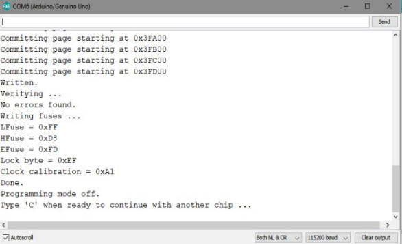
The board is NOT in the S100 bus. Make sure you get a "No errors found" return in the Serial Terminal feedback.  BTW, the LCD display will light up drawing power from your USB connection if it is soldered directly to the board.  It does not seem to affect the programming process. I do like to remove power to the Micro SD card adaptor (P52),  however at this stage.

Next we will repeat the above steps we did for the 328 CPU to check our bootloader is fine. 
Again we will test it with BLINK_2560.INO.

Using the SparkFun FT231x Serial to USB adaptor in P28,  make sure the jumpers  P41, 4-5,  P47, 4-5 and K5, 1-2 are still there. 
Make sure the two jumpers on P50 are still connected to pins 4 & 5 of P32 (as they were for the above 328 CPU LED blink test).

Insert the board into your S100 chassis and power it on.
Check the USB cable from the SparkFun FT231x to your PC's USB port has the correct COM port. Within the Arduino IDE "Tools Menu", set the Arduino board type to MEGA 2560.

Compile and upload the "sketch" BLINK_2560.INO program.  During the upload the LED's on the FT231x board should flash.  Also the D4 LED should light up.  If this does not happen you probably either have an invalid boot loader or a bad USB port connection. 

If the BLINK_2560.INO program worked the LEDs D3 & D2 should blink.  If not and you have a genuine Arduino MEGA 2560 upload the BLINK2560.INO program to that unit and check that the boards "Shields Pins" 2 & 3 pulsed high/low continuously.  You can use a resistor/LED as a probe.   Here is a picture of the board at this stage.
    
     Step 7
     
   
LCD Display Using the MEGA 2560 CPU
With that working and our bootloader OK, now lets get the LCD display working.
With the display still in its P6 socket, for our 2560 CPU we will drive the display with the CPU pins
37-42 (PL2,PL7, PL3-PL6).
So for
P51 remove all the jumpers.  For P12 the jumpers 1-2, 3-4, 5-6, 7-8, 9-10 & 11-12 should remain in place.
We have nothing else to change except the Arduino Sketch library values for the relevant pins.
Compile and upload the LCD_2560.INO file:-

LiquidCrystal lcd(42,47,43,44,45,46);        // CPU pins 42,37,41,40,38,38 (PL7, PL2, PL6, PL5, PL4, PL3)

void setup() {
        pinMode(WRITE_LED, OUTPUT);
        pinMode(READ_LED, OUTPUT);
        lcd.begin(16,2);                     // set up the LCD's number of columns and rows:
        lcd.clear();
        lcd.print("LCD Initilized.");
        lcd.setCursor(0,2);
        lcd.print(FreeRam(),DEC);
        lcd.print(" Bytes free");
    }

We will use this LCD display to issue diagnostic information about the board to us as we progress further.
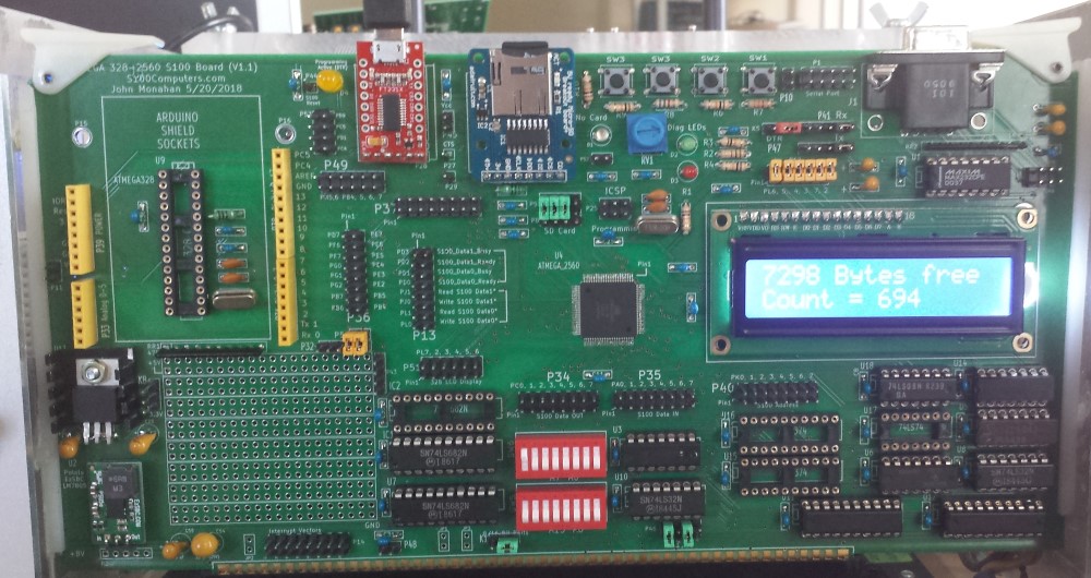
Note how the "Bytes of Free RAM is ~7K with this CPU rather than ~1K for the 328 CPU.
Note the LED D2 & D3 should be flashing.
Here is a picture of the board at this stage:-
     
  Step 8
     
SD Card Interface using the MEGA 2560 CPU

Next we will again add (or reactivate) the Micro SD card adaptor with our MEGA 2560 CPU. Insert the SD card adaptor (again) in connector P7.
With this arrangement the MicroSD card needs to be connected to the 2560 CPU pins (19-22). 
The required jumpers are 
P9-1 to P8-1, P9-3 to P8-2,  P9-5 to P8-3 and P9-7 to P8-4, (PB0-PB3).  
Make sure power is getting to the card with jumper P52.
Insert a MicroSD card.  The D1 LED should go off.

Again we will test our card with 3 simple sketch programs derived from the Arduino IDE "SD Card" examples.
Again we launch the Arduino IDE serial terminal interface with the boards USB port.  It's Baud rate should still be 115200.

This time the 2560 CPU hardware pins 19-22 are the Arduino sketch library pins are 50-53 so we need to compile and upload SDCardInfo_2560.INO.   Note the fact that we set the "Tools/board" option in the Arduino IDE menu to "MEGA 2560" automatically takes care of this for us. We just need to set the CS* pin. We will use the 2560 CPU pin 19 (Library #53) for SS.
You should then see the same information in the "Serial TTY window" we saw above:-
    
  SD Card Info 2
   
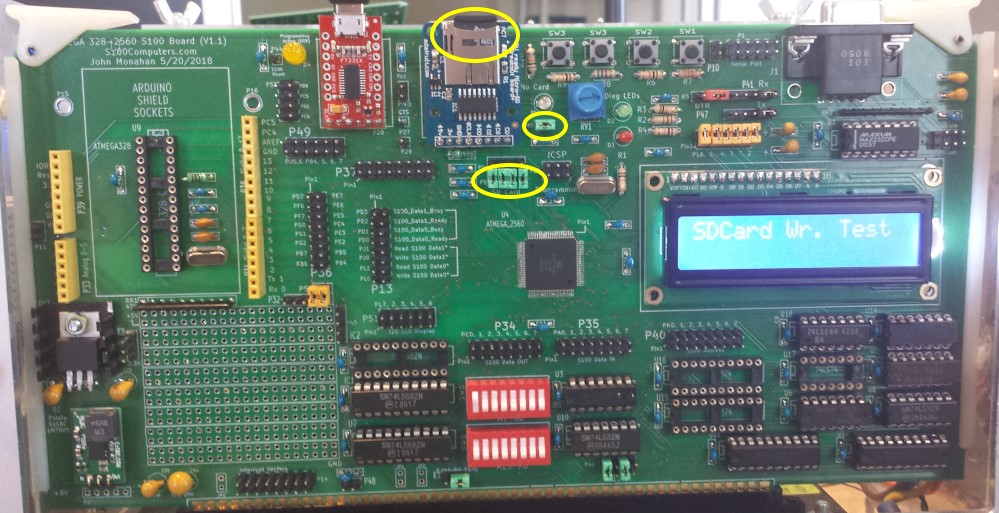
Likewise to read and write to the TEST1.TXT file on the Micro SD card run SDCardWrite_2560.INO and SDCardRead_2560.INO.
Here is a picture of the board at this stage:
       
  Step 9
      
     
S100 Bus IO with the MEGA 2560 CPU
OK, we now have our board to roughly the point where we had it with the original 328 CPU. Unlike that situation however, there are many more available GPIO pins to interface with the S100 bus with the 2560 CPU.  However we need to get a few things straight. First, remember all pin naming will be in terms of the Arduino MEGA 2560 board. We will always use the Arduino IDE interface with the MEGA 2560 as the target board.  This will automatically assign the correct library pin names with the actual CPU hardware pins. Again for some reason there are a number of 2560 CPU GPIO pins that Arduino does not use on their MEGA board.  They are also not designated in the IDE sketch library.   I have brought them out to Jumper block P37.  Perhaps the could be utilized with a more sophisticated IDE such as Atmel Studio 7.

Second, there are two ways S100 bus ports are addressed on this board. Either hardwired using the dip switches SW5 and SW6 (as we did for the 328 CPU) or by inputting the S100 bus address lines directly into the 2560 CPU GPIO lines itself.  We will  start with the simplest case, the hardwired setup. 

S100 Bus Port Read
First add all the remaining IC's to the board, including the MAX232 serial interface chip.   Do not remove any of the pin jumpers.
For simplicity will assume (here) that the upper 8 bits are zero and the port address is
80H as we did for the 328 CPU, so  the dip switches SW5 & SW6 should not be changed.
This time however we will be able to work with complete byte wide data, and we can utilize the Arduino IDE script to input 8 bits as one unit (if the designated CPU pins are contiguous).  On this board the default arrangement will be:-

S100 bus data in (to the 2560 CPU, from the S100 bus) is via pins 78-71 (PA0-PA7), using jumper block P35.
S100 bus data out (from the 2560 CPU, to the S100 bus) is via pins 53-60 (PC0-PC7), using jumper block P34.
The S100 address lines A0 to A7 will be presented to the 2560 CPU via pins 89-82 (ADC8-ADC15), using jumper block P40.

 
We will hookup the eight S100 bus data
IN pins to the 2560 CPU pins 78-71 (PA0-PA7) by jumpering all the pins in P35 (1-2.....15-16). The relevant S100 data bus buffer is U11.
Note the "
IN & OUT " designations here and below refer to data as far as the 2560 CPU is concerned, not the S100 Bus CPU. 
We will
IN S100 bus data that is on the S100 bus data OUT lines.
While we are at it, hookup the eight S100 bus data OUT pins to the 2560 CPU pins 53-60 (PC0-PC7) by jumpering all the pins in P34 (1-2.....15-16), we will use them later.
Also jumper P40 1-2, 2-3.... 15-16 we will use these CPU pins later when we want the CPU to define an I/O port (see below).

When the
S100 bus writes to port 80H it will set the S100_DATA0_READY pin 5 on U14A HIGH via U5D (as we did for the above 328 CPU).  
This is routed to Pin 8 of P13 and via a jumper to
P13 pin 7 it will end up on the PD0 pin 43 of the CPU.
Likewise the
READ_S100_DATA0 signal from pin 36 of the CPU (PL1) will via P13, jumper 13-14 reset the U14A FF (its pin 1).
Compile and run the Arduino sketch program
S100_Port_Rd_2560.INO
Boot up your Z80 monitor and send the value 13H  to port 80H.

QO80,13

You should see this value on the LCD display.
Here is a picture of the board at this stage.   
          
  Step 10
    
Here is the core of the Arduino Sketch code:-

void setup() {
DDRA = 0b00000000;                             // Set CPU pins 78-71 as Input (8 bits wide)
PORTA = 0xFF;                                  // enable all pull-ups

......
}

void loop() {
if (digitalRead(S100_DATA0_READY))
    {
    lcd.clear();
    lcd.print("READY = TRUE ");
    lcd.setCursor(0,2);
    lcd.print("Port 80H = ");
    digitalWrite(READ_S100_DATA0, LOW);        // latch and hold data bit
    x = PINA;                                  // Read all a bits (CPU Pins 78-71)
    digitalWrite(READ_S100_DATA0, HIGH);       // we are done, release 74LS374
    lcd.print(x,HEX);
    digitalWrite(READ_LED, LOW);               // Flash READ LED
    delay(500);
    }
lcd.clear();
lcd.print("READY = FALSE");
lcd.setCursor(0,2);
lcd.print("Port 80H = ");
lcd.print(x,HEX);
digitalWrite(READ_LED,HIGH);
delay(500);
}


You will need to read up a little on Arduino programming to understand some of the above code.  Blocks of pins (8 bits wide) are given special names in these Arduino scripts. So
PINA is a block of 8 contiguous pins (78-71) on the CPU. Likewise for DDRA and PORTA.
 
S100 Bus Port Write
Next we will write to the S100 bus port 80H.
When the
2560 CPU writes to port 80H it will latch the data into U12 pin 11 with WRITE_S100_DATA0*.
This signal will also  the S100_DATA0_BUSY pin 9 on U14B HIGH.  
This is routed to Pin 6 of P13 and via a jumper to P13 pin 5 it will end up on the PD1 pin 44 of the CPU.
When the port is read on the S100 bus side
INO* goes low resetting the U14B FF.
The 2560 CPU should not send another byte while  S100_DATA0_BUSY is HIGH
The
WRITE_S100_DATA0* is generated on pin 35 of the 2560 CPU (PL0) so we jumper P13 15-16.

Compile and run the Arduino sketch program
S100_Port_Wr_2560.INO
Boot up your Z80 monitor and read the value to the S100 bus port 80H.  It should match with the value on the LCD display.

QI80, 00000000
QI80, 00000001
QI80, 00000010
QI80, 00000011
etc.
 
Here is the core of the Arduino Sketch code:-

void loop() {
   READY = digitalRead(S100_DATA0_BUSY);
   digitalWrite(WRITE_LED,READY);                // Show status of READY LED
   if(!READY)
      {
      lcd.clear();
      lcd.print("80H BUSY = FALSE");
      PORTC = x++;                               // Write all a bits (CPU Pins 53-60)
      digitalWrite(WRITE_S100_DATA0, LOW);       // latch and hold data bit
      digitalWrite(WRITE_S100_DATA0, HIGH);      // we are done, release 74LS374
      delay(300);                                // Allow time to read LCD display
      } else {
      lcd.setCursor(0,0);
      lcd.print("80H BUSY = TRUE ");
      lcd.setCursor(0,2);
      lcd.print("Next Byte = ");
      lcd.print(PORTC,HEX);
      }
}
  
Again if you do not see this value back trace with a logic probe and determine why.
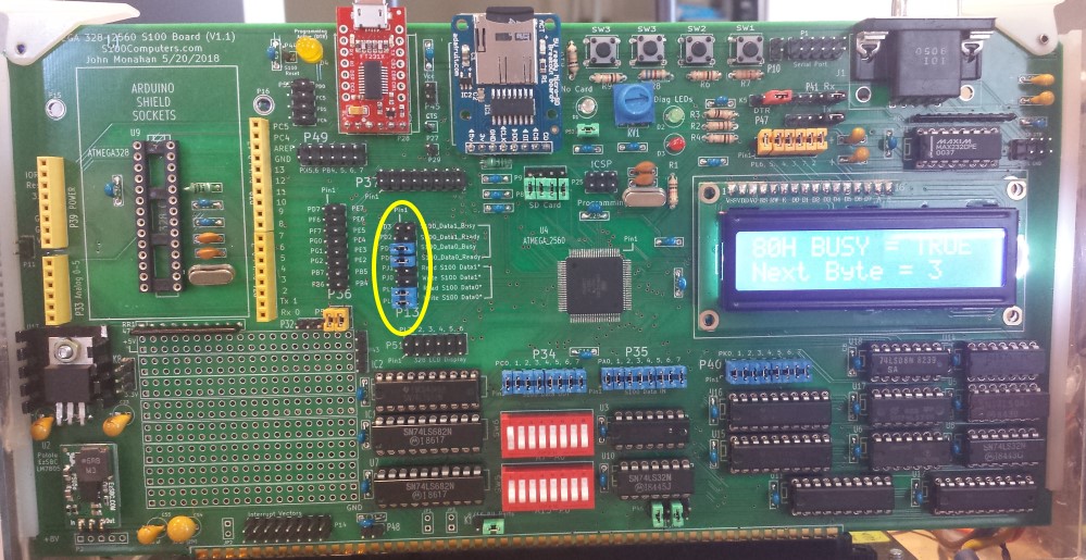
Here is a picture of the board at this stage:
    
  Step 11


S100 Bus Read/Write from a Atmega 2560 Defined Port(s).
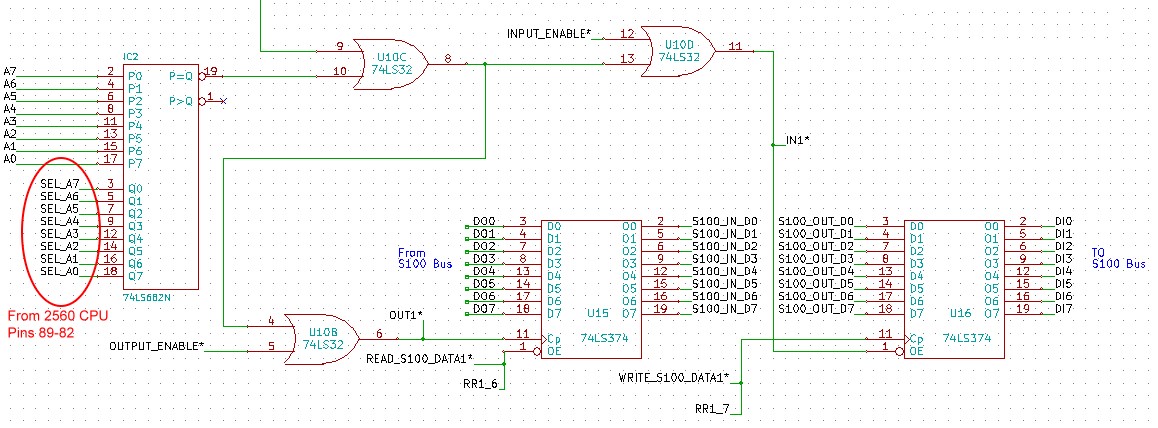
We are almost there!   Next we would like the Mega 2560 CPU to be able to define the actual S100 bus port(s) being addressed.   If you examine the boards schematic you will see that there are two separate pairs or port I/O buffers that interface with the S100 bus. Up until now we used the 74LS682 and SW6/SW5 to define the S100 bus port. We will now use the PK0 - PK7 pins on our 2560 CPU to define the S100 port(s).  Here is the relevant circuit.
      
   Port Selection
   
Jumper P13 9-10 (
READ_S100_DATA1*) and 3-4 (S100_DATA1_READY).
We already have the P40 jumpers installed (see above), which allow the CPU pins 82-89 to define the port address going into IC2.

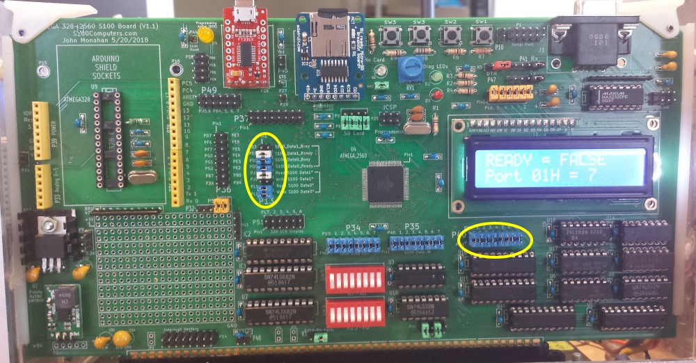
We will repeat the above S100 Port read program but this time we will use the Propeller Console Board Keyboard I/O port (01H) as the test port.

Compile and upload S100_Port_
Rd2_2560.ino within the Arduino IDE.
Within your Z80 monitor, go to the "Type characters command T" then enter any keyboard character you like.
You should see something like this same character on the LCD display. In the example below "2".
     
    Step 12
      
Here is the core of the Arduino Sketch code:-

void setup() {
     DDRK = 0b11111111;                         // Set CPU pins 89-82 as Outputs (8 bits wide Port Address)
     DDRA = 0b00000000;                         // Set CPU pins 78-71 as Input (8 bits wide)
     PORTA = 0xFF;                              // enable all pull-ups
     ......
     PORTK = 0x01;                              // Set port address to 01H (CPU Pins 53-60)
}

void loop() {
if (digital Read(S100_DATA1_READY))
     {
     lcd.clear();
     lcd.print("READY = TRUE ");
     lcd.setCursor(0,2);
     lcd.print("Port 01H = ");
     digitalWrite(READ_S100_DATA1, LOW);        // latch and hold data bit
     x = PINA;                                  // Read all a bits (CPU Pins 89-82)
     digitalWrite(READ_S100_DATA1, HIGH);       // we are done, release 74LS374
     lcd.print((char)x);

     digitalWrite(READ_LED, LOW);               // Flash READ LED
     delay(500);                                // Allow time to read info
     }
lcd.clear();
lcd.print("READY = FALSE");
lcd.setCursor(0,2);
lcd.print("Port 01H = ");
lcd.print((char)x);
digitalWrite(READ_LED,HIGH);
delay(500);
}


Finally
we will output to an S100 port again using the Atmega 2560 to define the port. This is essentially the same code as we had for the above SW5/SW6 defined port (80H). 
This time lets set the output port to 40H in the Arduino code. 
Jumper P13 11-12 (WRITE_S100_DATA1*) and 1-2 (S100_DATA1_BUSY).
Compile and upload S100_Port_
Wr2_2560.ino within the Arduino IDE.
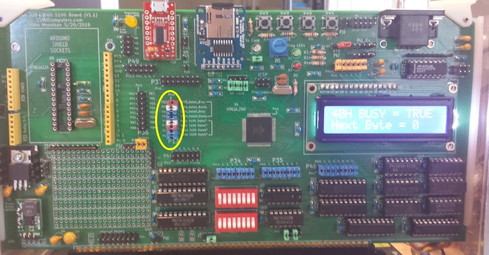
You should see the following text on the LCD display with the monitor commands:-

QI40, 00000000
QI40, 00000001
QI40, 00000010
QI40, 00000011
etc.

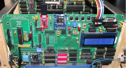
Here is a picture of the final board setup
     
 
     Step 13

Here is the core of the Arduino Sketch code:-

void setup() {
    DDRK = 0b11111111;                          // Set CPU pins 89-82 as Outputs (8 bits wide Port Address)
    DDRC = 0b11111111;                          // Set CPU pins 78-71 as Outputs (8 bits wide)

    pinMode(READ_LED, OUTPUT);                  // RED
    pinMode(WRITE_LED, OUTPUT);                 // GREEN
    pinMode(S100_DATA1_BUSY, INPUT);
    pinMode(WRITE_S100_DATA1, OUTPUT);
    .....
    PORTK = 0x40;                               // Set port address to 40H (CPU Pins 53-60)
}


void loop() {
    READY = digitalRead(S100_DATA1_BUSY);
    digitalWrite(WRITE_LED,READY);              // Show status of READY LED
    if(!READY)
       {
       lcd.clear();
       lcd.print("40H BUSY = FALSE");
       PORTC = x++;                             // Write all a bits (CPU Pins 53-60)
       digitalWrite(WRITE_S100_DATA1, LOW);     // latch and hold data bit
       digitalWrite(WRITE_S100_DATA1, HIGH);    // we are done, release 74LS374
       delay(300);                              // Allow time to read LCD display
       } else {
       lcd.setCursor(0,0);
       lcd.print("40H BUSY = TRUE ");
       lcd.setCursor(0,2);
       lcd.print("Next Byte = ");
       lcd.print(PORTC,HEX);
}

 
Other 328-2560 Board components.
This completes the configuration of the S100 ports section tests.  Please note the above programs are extremely rudimentary.  Practical programs would probably use all four S100 buffers, multiple ports and perhaps also utilize S100 interrupts (available on P32) as well as "Arduino Shields".  There is ample space within the Atmel 2560 CPU Flash RAM to run quite large programs.   If you do write programs that you think might be of general use please send them to me for posting on this page.

The RS232 Serial DB9 Port Interface
Sometimes, the above USB serial port just isn't enough or you need to use an old fashioned  RS232 Serial connection.  The MEGA 2560 CPU has in fact 3 possible serial connections:-

Rx0 pin 2     Tx0 pin 3     (Used by the FT321x USB board, P28).
Rx1 pin 45   Tx1 pin 46
Rx2 pin 12   Tx2 pin 13
Rx3 pin 63   Tx3 pin 64   (Used by the MAX323/RS232 interface, U1)


While any of the above pairs can be used the jumper arrangement is easiest using the Rx3/Tx3 pair.
We will setup a simple PC based TTY terminal to communicate with the RS232 serial DB9 socket J1.    This circuit is essentially the same as we used for our PDP11 CPU board serial connection.
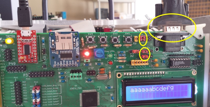
First jumper P41 2-3 and P47 2-3. Jumper P1 1-3 and 2-4.
We will bypass the P1 socket for the moment and use the onboard DB9 standard socket.  The P1 socket is only if you need to bring the serial connection to the back of your system box and put the cover on it.

Connect a serial connection to a TTY terminal on your PC to the top DB9 connector J1.  There are many programs. I like "Absolute Telnet" but the free PuTTY one is also excellent.  We will start the serial connection to this board as, 115200 baud, 8 data bits, 1 stop bit, and no parity.   Most modern PCs today only have USB serial ports, so you will need a USB to Serial cable connector. Almost any type will work for this simple application.
 
Bring up your PC TTY interface.  Make sure the transmit character echo is off.
Compile and run the
RS232_2560.INO sketch program (see below).
Anything you type (send) from your PC TTY interface should be echoed back on the same interface from the serial interface/2560 CPU on this board and also appear on the boards LCD display. You can also bring up the Arduino IDE serial interface and see the same output (when you type in the PC TTY window).
Here is the core sketch code

void setup() {
     pinMode(TxD3, OUTPUT);                // RS232 OUT
     pinMode(RxD3, INPUT);                 // RS232 IN
     Serial3.begin(115200,SERIAL_8N1);     // Serial 8 bits, No parity, 2 stop bits
     .......
}


void loop() {
     if (Serial3.available()) {            // read from port 3, send back to port 3
     DataByte = Serial3.read();
     digitalWrite(READ_LED, LOW);
     if(++cursor_position > 15)
         {
         cursor_position = 15;
         lcd.scrollDisplayLeft();
         }
      lcd.print((char)DataByte);
      Serial3.write(DataByte);
      digitalWrite(READ_LED, HIGH);
      }
}

This circuit is fairly easy to debug.  First check your PC serial connection is working -- use something like out PDP11 board/monitor to check it out.  You should initially see a single pulse on pin 11 of U1. Typing any character on your PC should pulse 9 of U1.  Remember the RS232 signals themselves can be at least +/- 12 volts if you use a logic probe.  Here is a picture of the board at this stage.
  
  Stage 14
    
  
The Push Buttons Interface
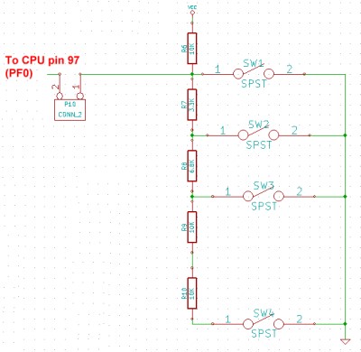
Often its nice to have multiple push buttons to control a programs flow.   While this can be easily done with high/low inputs to multiple CPU GPIO pins, a number of buttons can use up valuable GPIO pins.  We can take advantage of the fact that the 2560 CPU has a number of analogue GPIO pins and use only one GPIO pin to have (at least) 4 pushbutton inputs.   Here is the relevant circuit.
  
   Push Buttons

We will measure the voltage on PF0 (CPU pin 97) to determine which button was pressed.
We need to insert jumper P10.
Compile and run the Buttons_Test_2560.INO sketch program (see below). As each switch is pressed the LCD will indicate the correct switch.
Here is the core sketch code

void loop()
    {
    do {                                                         // wait for a button
       AnalogIn = analogRead(ANALOG_INPUT);
       delay(10);
       } while(abs(AnalogIn - analogRead(ANALOG_INPUT)) > 8);    // wait until reading does not change

     key = KEY_NOT_PRESSED;

     if(AnalogIn < 896) key = KEY_SW1;
     if(AnalogIn < 640) key = KEY_SW2;
     if(AnalogIn < 384) key = KEY_SW3;
     if(AnalogIn < 128) key = KEY_SW4;

     switch(key)
           {
           case KEY_SW1:
                  lcd.clear();
                  lcd.setCursor(0,0);
                  lcd.print("SW1 Pressed ");
                  digitalWrite(WRITE_LED, LOW);
                  delay(100);
                  digitalWrite(WRITE_LED, HIGH);
                  break;
           case KEY_SW2:

                 ........
           }
    }

Again the above few lines of code illustrate why the Arduino system is so popular.
There is a decent size "patch" area on this board to add your own custom circuitry.


MEGA 328 & 2560 CPU Bugs & Notes.
There are no bugs noted for this board currently. 

I have had varying success programming the 2560 CPU bootloader with other "burners" besides the UNO approach I described above (and highly recommend).   One I did get  to work was the
Pololu USB AVR Programmer V2 described here.  The nice thing about this unit is that it can be used to burn a bootloader and also upload a sketch program using only the 6 pin ISP connector (P25). You don't need to use the USP port/CPU pins PD0 & PD1.  Within the Arduino IDE tools/programmer,  select  "Atmel SDK development board".  Note this programmer requires 5V to the CPU via the S100 bus when burning the bootloader (i.e. Your S100 System switched on). 
      
Studio 7 Icon If you are up to it there is a much more sophisticated interface for the 328 & 2560 CPU chips provided free by Atmel called Atmel Studio 7. It can be downloaded here.  Programming however requires you to use their Atmel-ICE Debugger.  I have it but not used it. Seems like a pain to setup, Microsoft Visual C must also be resident on your PC for it to run.
   
Acknowledgement
Finally I would like to acknowledge that the initial layout of this board came from an excellent article written by Bela Torok where he describes a nice Arduino driven PDP11 TU58 tape emulator, see here

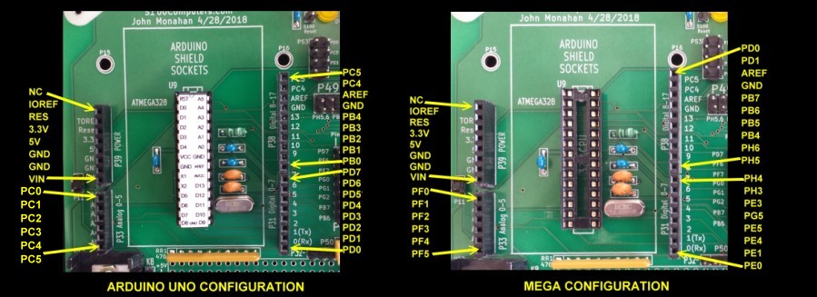
Shield Configurations
Please keep in mind that the "meaning" of pins in the Shields Sockets changes depending on whether the 328 or 2560 CPU is driving them.  It's unclear to me why the Arduino UNO shields were not made a subset of the MEGA shield sockets.  In any event here is how they are configured on this S100 board.
  
  Shields Configuration

Note the Mega Shields have further sockets not available on this board (see here).

Chips & Components.

Most of the components on this board are fairly standard and are available fro DigiKey, Mouser or Jameco etc.
The companies Adafruit, Pololu and SparkFun are excellent suppliers of the add-on boards/adaptors etc.

Board Configurations Submitted by users.
I will mentain here a list of board configurations submitted by users:-

 1. Harold Rothwell has submitted a nice implementation of a Time, Data, Temperature and Humidity display using the board with the 328 CPU.
       
  Please click on:-
DTH_DS1307.pdf
MY_INFO.INO
Harold Board


A Production S-100 Board
Realizing that a number of people might want to utilize a board like this together with a group of people on the  Google Groups S100Computers Forum, a "group purchases" is now open. If you would like such a board please reply on the forum.  Do not contact me directly.   A status list of board orders will be mentained here.

BTW, since there are two configurations of the board you might consider getting two boards.
The board(s) will be $16 + shipping. Payable with PayPal after you receive your board.


The links below will contain the most recent schematic of this board.
Note, it may change over time and some IC part or pin numbers may not correlate exactly with the text in the article above.

Atmega_Board_Programmer.ino                       (FINAL V1.11   6/21/2018)   
Mega_328_2560_Programming Files (.zip)       (FINAL V1.11  6/21/2018)   
Mega_328_2560 BOARD Schematic                        (FINAL V1.11   6/212018)                
Mega_328_2560 Board KiCAD Files (.zip)          (FINAL V1.11   6/21/2018)                
Mega_328_2560 BOARD Gerber Files (.zip)      (FINAL V1.11   6/29/2018) 
Mega_328_2560 BOARD Board Layout.pdf       (Provided by Rick Bromagem)        

Mega_328_2560 BOARD BOM.PDF                              (Provided by Rick Bromagem)
Mega_328_2560 BOARD BOM.XLS              
     (Provided by Rick Bromagem)


Other pages describing my S-100 hardware and software.
Please click here to continue...


This page was last modified on 11/17/2019