DAZZLER II Board
Theory Of Operation
Terry Walker 10/5/2016
The TV Dazzler 2 is intended to be a software compatible
plug-in replacement for the three board set consisting of the TV Dazzler DMA, TV
Dazzler Video, and D+7AI/O board set. This new board contains all of the
functionality of the original boards required to run the Dazzler Games programs,
plus additional capability for various video output modalities. All of the
small scale logic has been concentrated into three complex logic chips (CPLD)
with octal MSI parts used for bus signal buffers and address comparators.
A 4K byte static random access memory (SRAM) has been added to the board to
accommodate the display image area storage, so that the board does not have to
use direct memory access (DMA) to obtain the display from main memory.
This allows use of the board with any type or size of main machine memory.
The SRAM is configured as 'write only' so that whenever image data is written to
a portion of main memory, it is copied into this board's memory. Data read
back comes from the main memory. A dual port SRAM is used so that there
are no timing restrictions on the main memory bus speed or conflicts with the
display readout process.
The analog circuitry is simplified and uses commonly available parts to for the
ADC and DAC for analog I/O, together with simple video DAC output circuits.
The analog circuits to replicate the ADC and DAC use complex digital circuitry
embedded in a CPLD to simplify the required interface circuits. The ADC
input uses an external multiplexer, comparator, and 8 bit DAC to form a
successive approximation converter similar to the original D+7AI/O board.
The DAC outputs are made specifically for driving the speaker circuits in
joystick units and use pulse width modulated (PWM) circuitry in the CPLD
together with simple passive analog filtering to reconstruct the desired analog
output waveform.
The video output has been improved to have three separate 5 bit output DAC
circuits and two sync amplifiers to allow supporting VGA displays using a
standard HD15 connector. Choice of the video output mode is made with a
pair of jumpers on the board, and permits selecting four main video output
modes: 1) RGB or B/W display using standard TV scan rates, 2) RGB or B/W display
using VGA scan rates, 3) YPbPr three wire component video output at standard TV
rates, and 4) NTSC compatible composite color video on a single coax wire with
embedded color burst, chroma, and composite sync.
Inclusion of the analog interface circuits allows the TV Dazzler 2 to be a
single board solution for displaying and interacting with the original Dazzler
Games programs. Separately fabricated joystick units serve as the data
input interface, and the output can conveniently go to a 4 to 3 size ratio VGA
display of any size. If a more modern 16 to 9 ratio display is used, it
may not show the graphics output as a square unless the display operating mode
is properly set up. It has been possible to find copies of the .com files
for the original Dazzler Games which were written to run under the CDOS
operating system. These games ideally need small changes made for best
operation with this board under the CPM operating system.
DESCRIPTION OF THE OVERALL BOARD DESIGN
The entire schematic of the TV Dazzler 2 can be downloaded from
here.
The bottom left quadrant of the schematic contains the address comparators used
for choosing the base address of the various control ports and extended memory
address. There are also a set of octal parts used for buffering the S100
bus signals to the internal circuitry. Due to the large transients
sometimes experienced on the S100 bus, the signals cannot be connected directly
to the CPLD parts if best operating reliability is desired. Power supply
regulators to make +5V and -12V for the board are at the bottom center. A
Pololu switching regulator is used for the +5V source since the total board
current is in excess of 1.5 amps, and a linear regulator would have excessive
heat dissipation with heat sinking problems.
The large block at the left of center is the CPLD U3. This device contains
the bus interface control logic together with all logic associated with the
analog and digital functions of the joystick interfaces. The two analog
outputs for the joystick speaker amplifier inputs are at the left of U3 coming
from pins 5 and 6. These two pins contain high frequency PWM DAC signals
which are AC coupled and low pass filtered by the analog components to the left.
The maximum signal output is +/- 2 volts into a 10K ohm load and has 8 bit
resolution. A 10 MHz crystal oscillator to the upper left provides the
timing reference needed for the ADC and DAC operation.
Located to the right of the bus and joystick logic U3 is a dual port SRAM U2.
This memory chip has two sets of address and data lines which can independently
access the same block of memory cells. The left side connections go to U3
for data writing, and the right side connections go to U1 for image display.
Two options are possible for U2. Using a CY7C135 memory chip gives a total
of 4K bytes of storage, of which the TV Dazzler can display 2K bytes at a time.
In this case a jumper or extra output port can choose which 2K block of the SRAM
is displayed. Using an IDT 7132 SRAM memory chip give a total storage of
2K bytes, and this block is always displayed. The IDT chip is less
expensive and more easily obtained than the Cypress chip. The IDT chip has
the disadvantage that under certain software conditions, theoretically
interference between the reading and writing processes may cause glitches in the
displayed image. This has not been observed in practice.
Located to the right of the SRAM U2 is the display timing and readout logic,
which is contained in CPLD U1. This chip contains essentially all the
logic which was on the two boards of the original TV Dazzler, together with
additional logic to assist in generation of more accurate and more versatile
video output scan standards with accurate colors. The outputs of this chip
are three each 4 bit parallel DAC control lines and two sync pulse lines.
Since the outputs are CMOS with well defined voltage levels, they are used to
drive simple resistive DAC circuits to create the desired video signals.
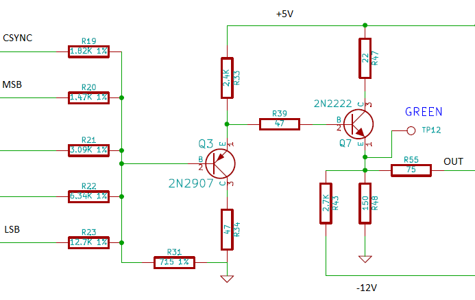
The resistive binary weighted DAC circuits are located to the right of U1.
Each consists of a resistive voltage adder with binary weighting followed by a
cascaded emitter follower to provide enough current to drive the terminated
coaxial line outputs. One percent tolerance resistors are used to provide
best accuracy, but the circuit can be built with the closest 5% resistors
and achieve adequate performance. The DAC produces a 2.2 volt peak signal
when sync is included, and the cascaded PNP/NPN emitter follower has a gain of
0.9. So the video output at the test point is 2V P-P, giving a 1V P-P
output into a 75 ohm termination. Although this simple circuit has some
distortion it is adequate for a 4 bit DAC, and gives rise and fall times of less
than 20 nanoseconds.
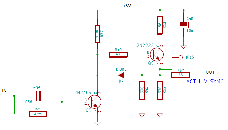
The two sync outputs have an inverting saturated amplifier followed by an
emitter follower. The resulting signal is about 4V P-P into an open
circuit, and half that into a 75 ohm termination.
Production of composite TV output video as provided by the original TV Dazzler
required more digital logic than U1 could contain. The optional CPLD U6 is
provided so that composite video may be accurately generated. The circuits
in U6 use digital synthesis for all voltage and timing levels so that when
composite video is output, it will meet the NTSC standards as used for TV
broadcasting. The original TV Dazzler did not have NTSC timing, and as a
result the video output could not be recorded reliably on video tape or viewed
on some modern TV displays. The TV Dazzler 2 composite video output is
compatible with any device which has a single coax composite video input.
This CPLD contains complex color encoder circuitry implemented entirely with
digital logic for accuracy and stability. As an aside, the intermediate
YPbPr signals are also available in one operating mode for driving standard TV
displays which incorporate YPbPr three wire component video inputs. When
using standard TV scan rates, YPbPr displays give much sharper images than
composite video signals. The IC U6 does not have to be installed unless
composite or YPbPr standard TV output is desired.
Located at the top of the schematic above U6 is an optional power converter P19,
which uses a CME0512C module to produce -12V from the +5V regulated power.
This power converter should not normally be installed. It was used for the
early PC board and CPLD development, allowing this board to run entirely on a
+8V DC input. In this case, the joystick units also had similar power
converters installed as will be described later, so they ran only on +5V also.
Do not install P19 for ordinary S100 bus usage.
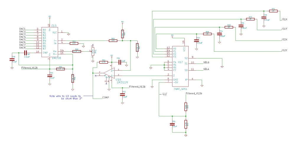
Located at the right center of the schematic is a group of 3 chips which
implements the ADC circuits needed for the joystick analog inputs. This
group is used in conjunction with logic in U3 to make a successive approximation
converter. Operation begins with the CMOS transmission gate switch U17,
which selects one of four analog inputs for conversion. Filtering networks
on the inputs provide some protection against input voltage transients and high
frequency noise. The normal signals at the switch inputs should be in the
range +/- 2.5V, with voltages up to +/-5V allowable without damage. Output
from the chosen channel input goes to one input of the comparator U16, which
will generate a signal to the CPLD indicating if the analog input is above or
below the signal generated by the DAC. The analog inputs have a high input
impedance, with only a small leakage current caused by the comparator input.
The feedback signal to the other comparator input is generated by an 8 bit DAC
using U15 and some passive components. An 8 bit control byte for the DAC
inputs DAC1-8 comes from an output of the CPLD U3. The reference for the
DAC comes from the -12V supply and the offset voltage from the +5V supply.
During normal operation the CPLD continuously selects one of the four analog
inputs at a time for conversion. The inputs are converted to the closest
two's complement digital representation and stored in memory in the CPLD.
When the CPU requests the value of an analog input, it is immediately available
and wait states do not have to be used. Otherwise the CPU might have to
wait up to 16 microseconds or more for the conversion to be done as was the case
with the original D+7AI/O.
In a similar manner, when the CPU writes an analog value to the two DAC outputs,
the 8 bit digital representation is stored in the CPLD and converted to the
analog speaker output voltage using a PWM DAC. This greatly simplifies the
external circuitry since devices like U15 do not have to be used for the speaker
audio outputs, and there is no wait state required.
DETAILED CIRCUIT DISCUSSIONS
A top level diagram of the logic in CPLD U3 is shown in
BLJ_ver1_top.pdf. The
equations in the CPLD files available separately implement the logic shown in
these schematics. There may be small errors in the schematic as shown
since it was drawn separately and not used for synthesis of the CPLD.
Input signals from the S100 bus come in at the left of the diagram and are
decoded by various gates to determine when ports are being accessed. A few
signals needed for the TV Dazzler control ports 0EH and 0FH are generated as
well as signals to control the bus interface ICs. The PWM block takes 8
bit signals from the JS1 and JS2 speaker output ports and generates a signal
repeating at 40KHz which has high to low level weighting proportional to the
desired signal. An external low pass filter recovers the audio signal for
the speaker amplifier.
The RAM address block takes in the 7 bit DMA starting address value and
subtracts it from the actual instantaneous address on the S100 bus. The
difference is tested to see if it is in the 2K byte TV Dazzler memory range, and
if so, outputs modified address bits 9 to 11 for the SRAM together with chip
enable signals for writing the S100 bus data to the SRAM.
The ADC scanner interfaces with the external ADC analog circuits to form a
complete ADC system using a successive approximation register (SAR) operation
method.
BJL_ver1_adc_scanner.pdf shows the internal details of the ADC scanner
block. Operation begins with the separately generated 8 MHz clock being
divided down by 16 to make a 500 KHz clock for use by the ADC. This then
goes to a further divide by 16 which is the operation control for the ADC
operation. Each time the control count is zero, a start pulse is issued to
the SAR shift register to begin a conversion. The SAR register operates
the same way as an AM2502 TTL IC. Each 2 microseconds, the SAR register
outputs a new 8 bit combination which goes out the qsar[7:0] output to control
the voltage generated by the external DAC. This discussion should be read
in combination with viewing the external analog circuits shown here:-
Comparator U16 determines if the DAC output is above or below the chosen analog
input for each combination. The comparator signal comp is used to control
the bit combinations generated by the SAR. When the SAR has checked all 8
bits of the binary output, the result is written into a latch for later use. The
counter I4 controls which analog input is converted and therefore which latch
receives the results. When the CPU reads an analog input, the output
pbjsin[7:0] makes the appropriate latch contents available for input. The
sequence of scanning all four analog joystick inputs repeats at about 31 KHz, so
that for all practical purposes the joystick input values are instantaneous.
The CPLD U3 has outputs qsar[7:0] which are used by the ADC process as well as
the bus outputs LDI[7:0] for the converted data to input to the CPU.
Various miscellaneous inputs and outputs are used for controlling the operation
of the TV Dazzler as well.
Display_final4C_top.pdf
shows a top level diagram of the logic used in CPLD U1 for display generation
and control. Operation begins with the master clock input at 28.6364 MHz
at the top left. This clock is divided by 3.5 to produce an intermediate
clock of 8.1818 MHz used for all pixel and scan timing purposes. 28.6364
MHz is 8 times the NTSC color subcarrier frequency of 3.579545 MHz which used to
generate composite color signals. The 8 MHz clock is further divided to
make a 2.045 MHz clock for the basic byte data rate in 64 by 64 displays.
The divide by 130 counter then generates the horizontal line rate of 15.734 KHz
for standard TV and 31.468 KHz for VGA operation. The line rate is
further divided by 525 to make the 59.94 Hz vertical field rate required for all
display modes.
A sync decode logic block decodes the various horizontal and vertical times when
sync or color burst signals should be generated as well as the horizontal and
vertical unblanking times. Each time the horizontal line is unblanked, the
horizontal address generator starts running, generating pixel byte addresses for
fetching data from the SRAM. In a like manner the vertical address
generator creates the upper portion of the pixel byte address corresponding to
the display line being processed. The combined address is output at the
top right of the schematic to the right side of the SRAM. In addition, the
addresses are sent to a test pattern generator for when the user Test switch is
activated.
Memory byte data comes in from the SRAM at the top right and is converted to a
string of 4 bit nibbles corresponding to the pixels being displayed. The
nibble string then goes through a multiplexer set to determine if the test
pattern or the nibble image is being displayed, and whether the nibbles are
being interpreted as a 4 bit color code or the individual bits for display.
If a bit mapped image is being displayed, the color from port 0FH is substituted
for the nibble data according to the bit state.
Finally the nibble data goes through color map blocks to convert the 4 bit
nibble to a 12 bit RGB triad for the color to be displayed. The map
outputs are relatched for timing stability and to remove glitches, and then
output on the pins red(3-0), green(3-0), and blue(3-0) to drive the external
resistive video DAC circuits. In addition, the nibble data before the
color maps is output on the lines disp(3-0) for use by the composite color
encoder circuits in the separate CPLD U6. Miscellaneous gate logic at the
bottom of Figure 5 produces the various sync signal outputs needed based on the
outputs of the sync decoder discussed previously.
Note that the video DAC drive signals are tristated by the mode1 signal, so this
chip's output is not used to drive the video DACs unless mode1 is low.
When mode1 is high, the video DACs are driven by U6 instead.
Display_final_3D_top.pdf
shows the top level diagram for U6. The chroma modulator block takes in
the pixel nibble codes disp(3-0) together with the 8 MHz pixel clock and the 28
MHz master clock. It internally derives the color subcarrier frequency
from the 28 MHz clock and uses it to modulate the output waveform with the color
difference signals. A set of color maps similar to the ones in U1 remap
the nibble codes into the color component values needed for NTSC representation.
These codes are output as the YPbPr 4 bit values for component TV operation.
In addition the component values are modulated onto the subcarrier to make the
chroma signal. When composite video is generated, the chroma subcarrier
signal is added to the Y signal used for component video to make the composite
video output. A sample of the subcarrier frequency is also added to the
component video output at the time of the burst enable pulse right after the
horizontal sync pulse on each line. Finally a set of multiplexers is used
to choose whether the DAC outputs are separately Y, Pb, and Pr; or all the same
as composite video signals according to the mode0 signal.
Note that the video DAC drive signals are tristated by the mode1 signal, so this
chip's output is not used to drive the video DACs unless mode1 is high.
When mode1 is low, the video DACs are driven by U1 instead. The tristate
technique permits the installation of U6 to be optional according to need.
If U6 is not installed and mode1 is high, the video DACs simply have no drive
and usually the display shows solid black or white.
Outputs from the digital video generators U1 and U6 go to the video DAC
circuits. Here is the video DAC used for the green channel:-
The red and blue DAC circuits are identical. The digital signals at the
left come from CMOS outputs generated by the CPLDs and are either 0 or 4V.
All signals are added together with a set of weighted resistors to produce the
final output voltage. The Csync is a negative going composite sync pulse
containing both horizontal and vertical synchronization signals similar to the
RS170 standard. Sync pulses are not present in all output signal modes.
The 4 bit digital color code on the MSB through LSB lines goes to a set of
binary weighted resistors to form a 4 bit DAC. Finally a resistor to
ground R31 is used to set the peak to peak (P-P) amplitude at 2.2 volts for
video plus sync. Transistors Q3 and Q7 are a PNP/NPN cascade emitter
follower with a gain into a terminated 75 ohm cable of about 0.9. The
final video into a 75 ohm terminated cable consists of 0.3 volts of negative
going composite sync with 0.7 volts positive going black to white range video
between the sync pulses. The PNP/NPN cascade is used since it provides first
order temperature compensation and adequate drive and distortion for this
application. This provides a non-loading amplifier for the resistive DAC
output to preserve the bandwidth and to separate DAC performance from loading
vagaries. The circuit is undamaged by output shorts and works fine into an
open circuit as well.
Here is the sync output buffer circuit used for both the Hsync and Vsync
outputs:-
A saturating switch with a fast transistor puts out a 5V amplitude pulse, which
is buffered by a high gain NPN emitter follower. The resulting voltage
swing at the Q9 emitter is approximately 4 volts, so if the output is connected
to a coaxial line terminated in 75 ohms, the pulse voltage at the load will be 2
volts. The output into an unterminated line will be 4 volts, and the 75
ohm resistor will absorb line reflections in that case to give a good pulse
shape at the far end.
Since the original port 18H output address is not being used on the D+7AI/O for
Dazzler Games, it is sufficient to use that port address for the Extra Port
implemented by U18. In the case that U18 is installed, be sure to remove
jumpers from P18 pin 3-4 (altmap), 5-6, and 31-32 (page) to prevent damage.
The video output mode is selected with a pair of jumpers on the board, and
permits choosing four main video output modes: 1) RGB, B/W, or bit mapped
display using standard TV scan rates, 2) RGB, B/W, or bit mapped display using
VGA scan rates, 3) YPbPr three wire component video output at standard TV rates,
and 4) NTSC compatible composite color video on a single coax wire with embedded
color burst, chroma, and composite sync. In case (1) with a B/W or bit mapped
display, all three video outputs are the same and an optional jumper (P18 3-4)
will put composite sync on all outputs. When an RGB output is generated
normally composite sync is only on the green output, but separate H and V sync
is also available. In case (2) the standard VGA mode of operation is done
with H and V sync on separate outputs. In case (3) the Y output has
composite sync included, and the Pb and Pr outputs are bipolar signals with a DC
offset. In case (4) all three outputs are the same.For additional
information on the TV Dazzler, D+7AIO, and joystick operation have a look at
these references: D+7AIO.pdf, and
here,
dac0800.pdf,
Cromemco
Dazzler Manual 1979.pdf.
Other pages describing my S-100 hardware and software.
Please
click
here to continue.This page was last modified on
10/07/2016