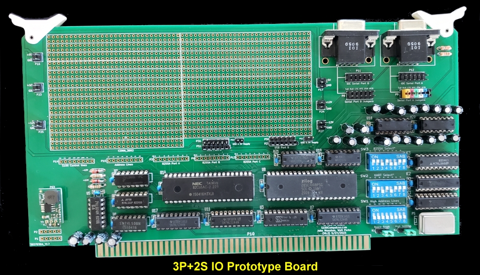
The 3P+2S IO Board
Introduction.
S100Computers has a
number of well established IO boards by now. All are fairly well debugged
and seem to function correctly. Some are almost 10 years old by now. Since
that time the have been a number of advances in small computer interfaces.
Boards like the Raspberry Pi or Arduino series have revolutionized computer
interfacing. Many add-on "modules" have been developed that allow
quite powerful computer setups.
There is no reason why these modules cannot be incorporate into S100 Bus
Systems as well. We have here a new IO board with 3 parallel ports and
2 serial ports. The board has a large "patch" area where the
user can use these ports to add various components such as sound generators,
serial terminals etc. It has the following capabilities.
1. Two generic RS232 Serial port capable of operation up to
115,200 Baud
with a DB9 Connector or a 8X2 Ribbon Cable Pin Connector
2. Alternatively one or both Serial ports can be used with
Serial to USB port adaptors
3. Three 8 bit parallel ports.
4 Only two sets of
S100 bus ports
are utilize. These are four 8 or 16 bit contiguous ports.
6. A large "patch area" is on the board to add other
components/modules
7. Important S100 bus control lines are available near the
patch area.
8. A simple program is supplied to test the board is
provided.
For the serial port the
default baud rate for this connection is
19,200 BAUD,1 stop bit, no parity
(19,200 BAUD 8N1).
This can easily be changes in software
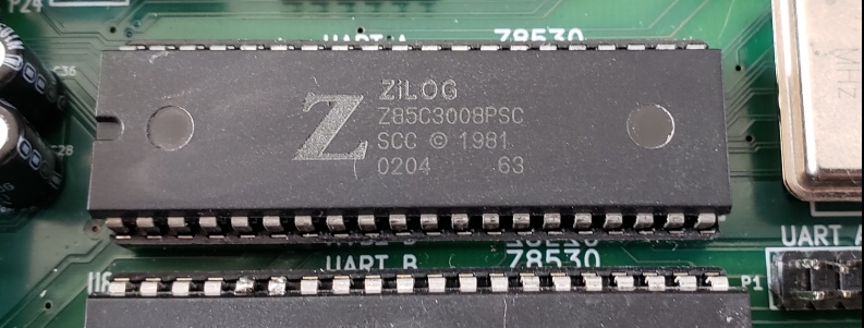
It is absolutely essential you use a Zilog
85C30's. I could not get the board to
work with other UARTs such as the OKI equivalent. The reason for this is
unclear to me.
Don't start this project without this chip.
Step By Step Building the
Super IO Board
The build instructions are fairly simple for this board
however building it should not be rushed. As always, first examine the bare board carefully for scratches or damaged traces, use a magnifying glass if need be. A broken trace is almost impossible to detect by eye on a completed board.
Solder in all the required IC sockets, resistors, resistor arrays,
capacitors and jumpers. The 4.915 Oscillator usually is inserted wit its
own "Oscillator socket". However you can also use a 14 pin DIP socket.
Note there are two sockets for the Pololu 5V regulator. While the older ones
(D24V25F5) are still available
and use P1, it seems Pololu is suggesting users use the newer
D24V22F5's
(5V, 2.5 Amp) units, it has a different pinout, use this one in P2. Be sure you get the regulator correct. To be safe once inserted, check
the voltage in your system is a 5V with no chips yet inserted on the board.
You can also use the
EZ-SBC regulators. It is soldered into K3. These EZ-SBC regulators are currently cheaper and as best I can tell just
as good -- though they have a larger footprint however.
As a last resort you can even use an old 7805 regulator with a heat sink in
K3.
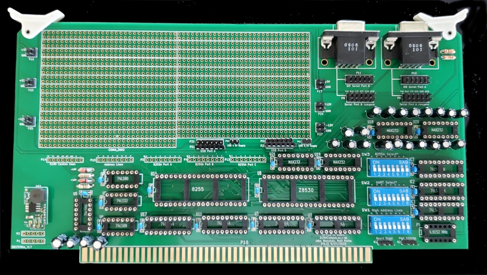
At this point insert the board into your system and check your S100 bus Z80 monitor
boots fine. If not check for solder bridges etc. Also do one last
check to be sure every IC solder pin is soldered. Seems trivial, but I
don't know how many times I got caught with this error.
Here is a picture of the board at this stage:-
Place the board in the S100 bus and check you are getting 5 volts on U5 pin
14.
Install all the 74LSxx IC's. Do not install the 4 MAX232 IC's yet
(U21,U19,U20 and U18). Install the 8255A (U14) but not yet the
Z85C30 (U8).
Jumper
K1 1-2, so the s100 bus reset line will
reset the 8255A configuration (see below).
PORT ADDRESSING.
This board utilizes two sets of ports. One set of 4 ports for the parallel ports
(the 8255A), and one
set of 4 ports for the serial ports (the Z8530) . Both sets utilize a
contiguous set of 4
ports.
This board has the ability to place the ports anywhere in the CPU's IO space
of 256 bytes, (or for 16 bit CPU 64K bytes).
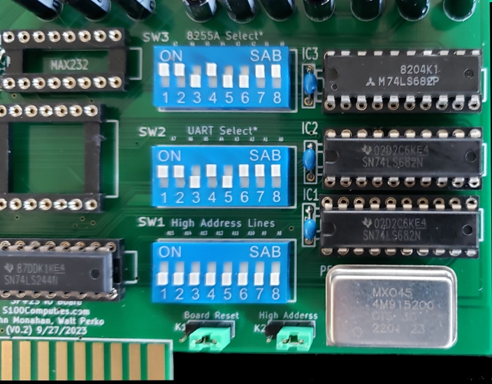
The tricky part is setting the dip switch jumpers for this.
To understand how this is done you should understand how the
74LS682 adders
selector chip works. Please read
here
There are 3 of them on this board.
IEEE-696 16 bit S100 bus port IO addressing is assumed (the upper 8 lines
being zero) for this board. This can be easily bypassed within the Jumper K2 1-2.
Do so if your 8 bit CPU board does not zero the high address lines for port I/O.
To be safe we will jumper K2 2-3 for now. Note 16 bit CPU's will probably require
K2 1-2.
Let us look
at how we set the dip switch settings.
SW1.
For now we will assume an 8 bit S100 bus master CPU, so for any IO port
address the address lines A15...A8 will all be low.
There eight all switches of SW1 should be closed (i.e. grounded). See the
schematic below. So jumpering K2 1-2 would insure the IC1 pin 19 output
(low) would get to pin 2 of IC2 and IC3.
To be safe for now we will bypass this option and simply ground K2 (pin
2-3). This in effect bypasses the use of SW1.
SW2.
This switch is used to set up the 4 ports for the Zilog UART (U8).
Pick a port range that is not already used in your system.
We
will use ports 50H (Port 1, control), 51H
(Port 0, control), 52H (Port 1, data) and 53H
(Port 0, data)
here, so Port 50H to 53H.
We must match the inputs of IC2 pins 2,4,6,8,11,13,15 and 17
to exactly match the switch settings of pins
3,5,7,9,12,14,16 and 18. Only then will
pin 19 of IC2 go low (and
select the UART).
Here is how things should match up:-
Upper Address, A7,
A6, A5, A4, A3, A2, GND
0 0
1 0 1 0 0
0 Port 50H to 53H
SW2 on on off on
off on on on
SW3.
This switch is used to set up the 4 ports parallel ports of the 8255A (U14). Pick a
port range that is not already used in your system.
We will use
ports 58H (Port A), (Port B), 5AH
(Port C) and 5BH
(Port D)
here.
Again we must match the inputs of IC3 pins 2,4,6,8,11,13,15 and 17
to exactly match the switch settings of pins
3,5,7,9,12,14,16 and 18. Only then will pin 19 of IC3 go low (and
select the 8255A).
Here is how things should match up:-
Upper Address, A7, A6,
A5, A4, A3, A2, GND
0 0
1 0 1 1 0
0 Port 58H to 5BH
SW3 on on off on
on on on on
Here is a picture of the DIP switch settings.
It may be confusing to see that pin 19 of IC2 and IC3 are always pulsing.
This is because only the address lines are fed into the chips. The
sOUT and sINP signals go directly to the 8255A or
Z85C30 and are internally AND'ed with CS*.
TESTING THE 8255A PARALLEL PORTS
We us a common 8255A IC to provide 3 parallel ports on the board. This
is a old IC but one of the most widely and reliable chips used for over 30
years. It's
a 40 pin IC with individual pins for three 8 bit IO ports. The catch
is the chip is somewhat tricky to setup because it has numerous modes in
which these pins can be utilized. Either output, input or bi-directional.
if you are not familiar with the chip you must read the spec sheet
here.
The fourth port (port D) of the 8255A is the important port that determines
the function of ports A, B & C. It is an internal port on the chip
with no external pins.
Here we will configure the 3 parallel ports (A,B, & C) on the chip
by sending 8 bits to its D port, (in our case
5BH).
We will configure the chip as:-
A output, B input, and C (bits 0-3) output,
(bits 4-7)input)
We do this by simply one time outputting to port
5BH 10001010b (8AH).
This configuration must be done after any power-up or reset of
the chip.
If for example you wanted the configuration to be:-
A input, B output,
and C (bits 0-3) output,
(bits 4-7)input)
You would do so by outputting to port 5BH 10011000b (98H).
There are numerous other ways to program the 3 parallel ports on this
chip. Please see
here.
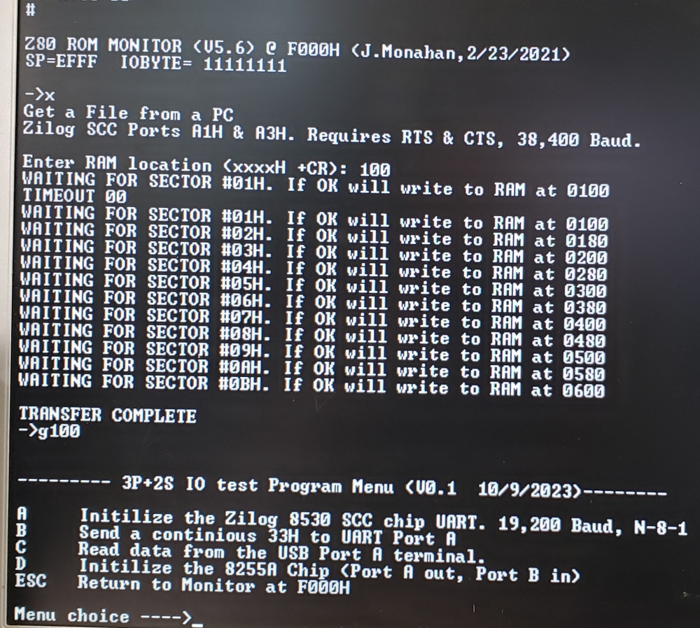
3P+2S_IO.Z80
In order to test the board I have written a small program 3P+2S_IO.Z80.
It can be obtained at the bottom of this page.
It runs at 100H and only uses the
Propeller Console
IO for input. This can be easily modified in the code if need be.
Here is the signon screen after transferring the .com file from PC
(with XMODEM):-
We will select menu item D. This will initialize and configure the 8255
and cause the 8 bits on its port A (pins 1-4 and 37-40) to continuously flip
0H to FFH.
Check this is happening wit a logic probe. Hit ESC to abort the test.
TESTING THE ZILOG 85C30 UART
Before installing the Serial circuit it might be useful to
review facts about the RS232 transmission protocol.
The RS-232 was originally introduced in 1960 for serial communication
transmission of data. It formally defines signals connecting between a DTE
(data terminal equipment) such as a computer terminal, and a DCE (data
circuit-terminating equipment or data communication equipment), such as a
modem. The standard defines the electrical characteristics and timing of
signals, the meaning of signals, and the physical size and pinout of
connectors. The RS-232 standard was commonly used in computer serial
ports and is still widely used in industrial communication devices. A serial
port complying with the RS-232 standard was once a standard feature of many
types of computers. Personal computers used them for connections not only to
modems, but also to printers, computer mice, data storage, uninterruptible
power supplies, and other peripheral devices. USB has displaced RS-232
from most of its peripheral interface roles. Thanks to their simplicity and
past ubiquity, however, RS-232 interfaces are still used—particularly in
industrial CNC machines, networking equipment and scientific instruments
where a short-range, point-to-point, low-speed wired data connection is
fully adequate.
Because the standard did not foresee the requirements of devices such as
computers, printers, test instruments, POS terminals, and so on, designers
implementing an RS-232 compatible interface on their equipment often
interpreted the standard idiosyncratically. The resulting common problems
were non-standard pin assignment of circuits on connectors, and incorrect or
missing control signals. The lack of adherence to the standards produced a
thriving industry of "breakout boxes", patch boxes, test equipment, books,
and other aids for the connection of disparate equipment. A common deviation
from the standard was to drive the signals at a reduced voltage. Some
manufacturers therefore built transmitters that supplied +5 V and −5 V and
labeled them as "RS-232 compatible".
In RS-232, user data is sent as a time-series of bits. Both synchronous and
asynchronous transmissions are supported by the standard. In addition to the
data circuits, the standard defines a number of control circuits used to
manage the connection between the DTE and DCE. Each data or control circuit
only operates in one direction, that is, signaling from a DTE to the
attached DCE or the reverse. Because transmit data and receive data are
separate circuits, the interface can operate in a full duplex manner,
supporting concurrent data flow in both directions. Note the standard does
not define character framing within the data stream or character encoding.
The standard specifies a maximum open-circuit voltage of 25 volts: signal
levels of ±5 V, ±10 V, ±12 V, and ±15 V are all commonly seen depending on
the voltages available to the line driver circuit. Some RS-232 driver chips
have inbuilt circuitry to produce the required voltages from a 3 or 5 volt
supply. RS-232 drivers and receivers must be able to withstand
indefinite short circuits to the ground or to any voltage level up to
±25 volts.
RS-232 devices may be classified as Data Terminal Equipment (DTE) or Data
Circuit-terminating Equipment (DCE); this defines at each device which wires
will be sending and receiving each signal. According to the standard, male
connectors have DTE pin functions, and female connectors have DCE pin
functions. Other devices may have any combination of connector gender and
pin definitions. Many terminals were manufactured with female connectors but
were sold with a cable with male connectors at each end; the terminal with
its cable satisfied the recommendations in the standard.
The following table provides a list of the major RS-232 signals and pin
assignment.
Direction is given with respect to the DTE - 'In' means the signal goes
to the DTE, 'Out' means it comes from the DTE; the signal names
also derive from this convention.
| Name |
Abbreviation |
Direction |
DB-25 pin |
DE-9 pin |
| Transmitted Data |
TxD |
Out |
2 |
3 |
| Received Data |
RxD |
In |
3 |
2 |
| Request To Send |
RTS |
Out |
4 |
7 |
| Clear To Send |
CTS |
In |
5 |
8 |
| Data Terminal Ready |
DTR |
Out |
20 |
4 |
| Data Set Ready |
DSR |
In |
6 |
6 |
| Data Carrier Detect |
DCD |
In |
8 |
1 |
| Ring Indicator |
RI |
In |
22 |
9 |
| Force Busy |
|
Out |
25 |
N/A |
| Signal Quality |
|
In |
21 |
N/A |
| Signal Rate |
|
Both |
23 |
N/A |
| Serial Clock Transmit |
|
In |
15 |
N/A |
| Serial Clock Receive |
|
In |
17 |
N/A |
| External Clock |
|
Out |
24 |
N/A |
| Signal Ground |
G |
Common |
7 |
5 |
| Protective Ground |
PG |
Common |
1 |
N/A |
The Request To Send (sometimes 'Ready To Send') and Clear To Send pair are
for hardware flow control, but use of them is fairly rare.
The signal ground provides a voltage reference for all the other signals,
and also serves as a common signal return for them.
In order to interface to the outside RS-232 world the zero or +5 volt
Low/High levels of the Zilog 8532 must be converted to the -12V & +12V
levels required for RS-232 transmission. In the 70's the two chips to do
this voltage level conversion were 1488' and 1489's. These worked fine
except you needed extra + and - 12 volt regulators. Today we use the +5
volt (only) MAX232 chips that internally generate the required voltages. So
the serial data I/O from the SCC pins goes through the MAX 232 chips to
convert the signals to RS-232 levels. (BTW one word of caution, be careful
with your logic probe if you are checking this circuit -- the MAX output
voltages are not TTL levels).
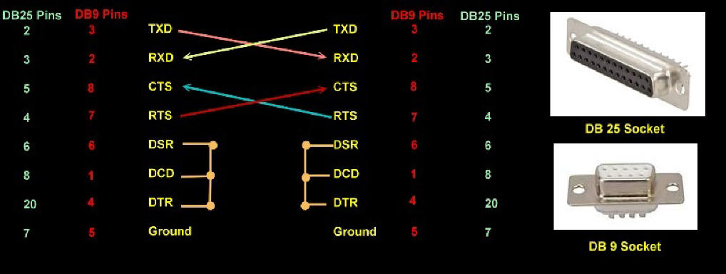
The most common pin connections between DTE and DCT is as follows.
The P8 and P9 jumpers on he board can be used to change the pinouts if
required.
The Zilog UART Chip
This is a more recent UART in the history of UARTs. It has the
advantage that it is totally self contained needing no other "support
chips" such as a Baud rate generator for example. It is a DUAL UART
allowing the use of two completely independent serial channels to be used.
There is almost no serial protocol it cannot work with. Finally it is
easy to program. You do so, by one time, sending a series of bytes to its
two control registers. Serial data is then continuously read from its
two data ports. The cost of all this flexibility is the task of
sending the correct configuration bytes to these control registers at the
start.
Please carefully read the spec sheet if you wish to reprogram the chip. It
can be obtained here.
Insert the Zilog 85C32, U8.
To make things simple here is the code to program the Zilog 85C30 port 0 to
19,200 Baud, N-8-1
(19,200
BAUD 8N1).
You would use the same code for the Zilog 85C30 port 1.
INIT$SCC:
LD A,ACTL ;Program Channel A of UART_0
LD C,A
LD B,0EH ;Byte count for below
LD HL,SCCINIT$A$A
MORE1:
LD A,(HL)
OUT (ACTL),A
INC HL
DJNZ MORE1
SCCINIT$A$A:
DB 04H ;Point to WR4 >>>>>>>>>>>>>>>>>>>>> (RS232 UART)
DB 44H ;X16 clock,1 Stop,NP
; DB 04H ;X1 clock,1 Stop,NP
DB 03H ;Point to WR3
DB 0C1H ;Enable
receiver, Auto Enable, Receive 8 bits
; DB 0E1H ;Enable
receiver, No Auto Enable, Receive 8 bits (for CTS bit)
DB 05H ;Point to WR5
DB 0EAH ;Enable, Transmit 8 bits
DB 0BH ;Set RTS,DTR, Enable. Point to WR11
DB 56H ;Receive/transmit clock = BRG
DB 0CH ;Point to WR12
; DB 40H ;Low Byte 2400 Baud
; DB 1EH ;Low Byte 4800 Baud
; DB 0EH ;Low Byte 9600 Baud
DB 06H ;Low byte 19,200 Baud
; DB 02H ;Low byte 38,400 Baud
; DB 13H ;low byte 115,200 Baud (With 1X clk)
; DB 00H ;Low byte 76,800 Baud
; DB 06H ;Try for 460800
DB 0DH ;Point to WR13
DB 00H ;High byte for Baud
DB 0EH ;Point to WR14
DB 01H
;Use 4.9152 MHz Clock.
DB 0FH ;Point to WR15
DB 00H ;Generate Int with CTS going high
Please study the
3P+2S_IO.Z80 to understand better how to use this
chip.
BTW, I have found the fast Z80 OTIR block output instruction does not
work reliably with some Z8530 UARTS.
To test the chip, insert the 85C30 in U8. Do not install the MAX232
chips yet.
First we will do a very simple test. We will send data out on Port A (TXD1,
pin 15), jumper it directly to (RXD1, pin 13).
We also need to connect RTS1 pin 17 to CTS1 pin 18.
Using the program above, first initialize the UART (Menu A).
Then select Menu B. This will continuously send a character out
through the UART pin 15 and receive it back on 13.
Check with a
logic probe that pin 15 and 13 are pulsing.
This must be the case before going further.
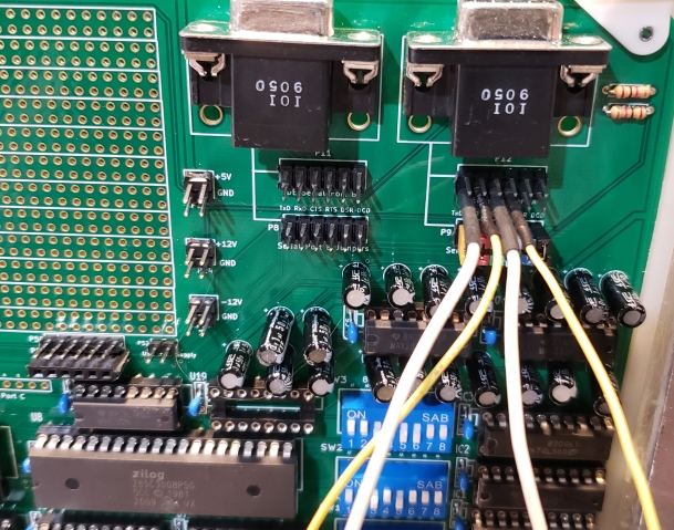
Next we will move the signal out to the MAX232's. Insert U21, U19,U20 and
U18.
Jumper P9 1-5 and 3-7.
Do the same Menu B check. Check you are getting a pulse U21, pin 14.
Here is a picture of the setup.
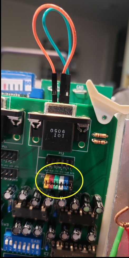
Finally we bring the signal out to the DB9 connector J2.
To do this all the vertical pins of P9 need to be connected.
Jumper the DB9 pin 2 to the DB9 pin 3
Jumper the DB9 pin 4 to DB9 pin 8.
Do the same Menu B check. Check you are getting a pulse U21, pin 14.
Here is a picture of the setup.
At this point if you have an RS232 terminal you should be able to
communicate with it at 19,200 Baud using the DB9 socket.
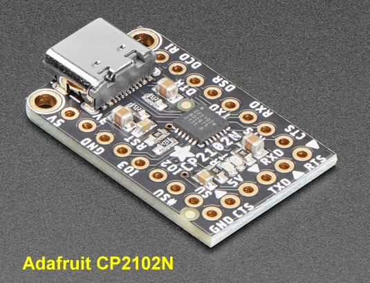
ADDING A USB PORT CONNECTION
These days a very popular way of communicating serial data is via a USB
connection.
Fortunately there are a number of simple modules these days to convert a 5V
serial signal to a USB signal.
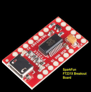
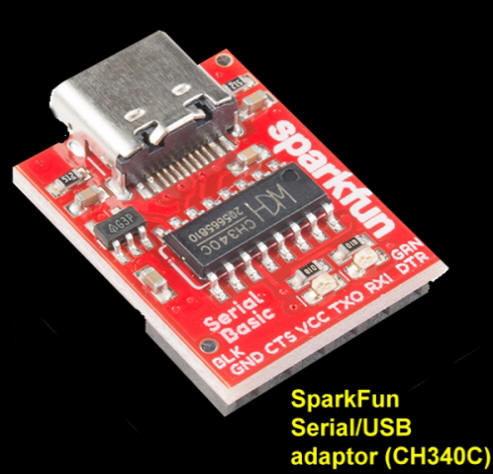
Here is a picture of three common ones.
The good news is they all utilize the same pinout along the bottom row.
Please read up on these adaptors on the Sparkfun or Adafruit web sites
before using them.
In order to utilize these adaptors on either or both UART ports the
corresponding MAX232 chips must be removed from the board.
UART port 0 utilizes P31 or 51. UART port 1 utilizes P50 or P20.
Both pairs of ports have the same pinouts. One can be for adaptors with pins
the other for adaptors with female sockets.
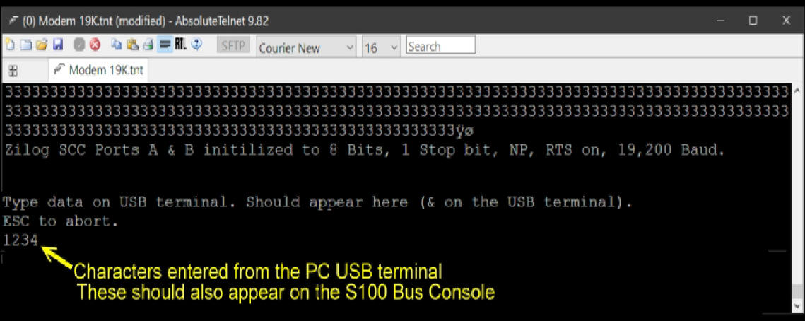
Also jumper P50 and if used P53.
For testing load the 3P+3S_IO program, Initialized the UART and run menu item
B.
The USB terminal (set to 19,200 Baud) should display 3's continuously
Next run menu item C. Anything you type on the USB terminal should
appear on your Z80 S100 bus console.
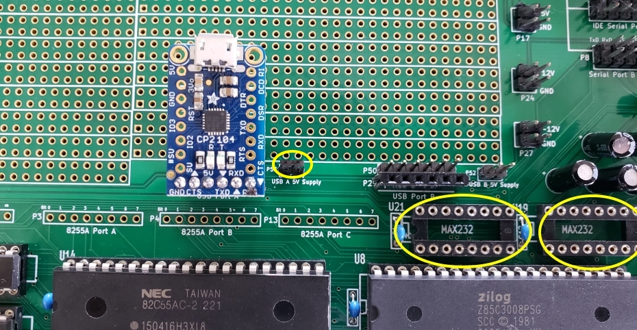
Here is a picture of the USB adaptor attached to the UART port A.
If these menu items all work you should have a functional Zilog 85C30 UART.
BTW, everything explained above works in an identical manner for the UART
port B
It's unclear to me why P50 (or P53) should be jumpered. This pin supplies
+5V from the USB PC connection.
Without it data entry on the PC terminal is not received by the USB module.
Here is what you should see on the USB terminal.
To Order a Production S-100 Board
A number of people may want to utilize
a board like this.
Together with a group of
people on the
Google
Groups S100Computers Forum, a "group purchases" will be setup on that
forum.
If you would like a bare board please keep an eye on that forum.
Please note some of the above pictures of the boards during the build
process are late stage prototypes. The position of certain items may be
slightly changed from the final (V1.0) versions.
The links below will contain the most recent schematic of the above boards.
Note, it may change over time and some IC part or pin numbers may not correlate
exactly with the text in the article above.
3P+2S_IO
Board Schematic
.PDF File (Note
V0.3), not yet available)
KiCAD files for
the 3P+2S IO Board .ZIP File (Note
V0.3 11/23/2023)
3P+2S_IO.Z80 (Text File)
(11/23/2023)
3P+2S_IO.Z80 folder (zip file)
(11/23/2023)
3P+2S IO
Board BOM (Text file)
(12/10/2023)
Other pages describing my S-100
hardware and software.
Please click
here
to continue...