S100 Computers

Home S-100 Boards History New Boards Software Boards For Sale
Forum Other Web Sites News Index    
  
An 8 MB Static RAM Board for our S-100 80386 &  80486 CPU Boards.
  
  Final 8MB Static RAM Board
   
  V3 RAM

INTRODUCTION
Please read up on the Master/Slave 80386 S100 board before reading this page.

The above 80386 CPU board worked fine with up to 16 MB of RAM in the S-100 bus and with a 32 MHz CPU clock input, (3 I/O & PROM wait states).   BTW, when accessing the S-100 bus (RAM or I/O) the CPU clock frequency is divided by four.  So the 80386 on the bus runs at 8 MHz.

In order to utilize the full addressing range capability (4GB) of this chip larger RAM boards are required.  Clearly the S-100 bus is not capable of meeting these addressing needs.  We solve this problem by adding, (one or more), daughter boards connected to our CPU board via two "over the top" ribbon cables.   This provides a local data bus by which the CPU can address as much RAM as it wishes in a 32 bit wide data path and at the full CPU's clock speed (32 MHz currently).  These special RAM boards draw only power from the S-100 bus. If needed other signals could be accommodated,  but in general they are transparent to the regular S-100 bus boards.

An Early SRAM Prototype RAM Board
The first attempt at the above concept was a 2 MB static RAM board. The schematic can be seen here. Below is a picture of this static RAM board. It was a kind of pre-prototype board (and just has 2 MB RAM) to test the circuits/concept.  It is in fact not even placed in the S-100 bus. Power was supplied to the board. 

When I connected up this RAM board via the top connectors/ribbon cable, it became apparent there were problems switching the clock speed from 8 to 32 MHz when one started accessing the static RAM board.  
    
  Per-Prototype RAM Board
      
However the above prototype board allows us to resolve and improve the clock switching circuit to the point that both are now very reliable with a 40MHz clock going into the CPU.  The basic problem was that the circuit that monitors address and checks for RAM above 16 MB (and so at higher speeds) must be latched. 
 
There was also a problem switching the CPU clock frequency when accessing the daughter board RAM in the above prototype. The circuit had to be modified such that a "runt" CPU clock cycle did not occur. Learning form the above prototype board we made a fourth 80386 prototype board and a 8MG Static RAM board.  Here is a picture of that board.  The schematic can be seen here.
    
  Final 8MG Static RAM
     
Both boards are connected together via two short overhead ribbon cable connectors as shown here. 
BTW, the ribbon cable shown here has only two boards.  This "
32-Bit S-100 Overhead Bus" is designed so multiple cards can be attached to it.
     
  RAM & CPU In Bus 
  
RAM Board Addressing
One thing that does take a little adjusting to is the sheer range of the addressing capability of the 80386.  We will later design a DRAM S100 daughter board for this CPU, but even the current 8MB static RAM daughter board here provides a significant play area to work with.  Setting up the address line configurations requires a little care.

The CPU board itself will always address RAM on the S-100 bus if that RAM lies within the first 0-16M of the 80386's address space.  This represents the maximum capacity of the S100 buss's addressing capability.   This would require four of our 4MB S100 bus static RAM boards (and many more of many older S100 bus RAM boards).

For any RAM above 16M, the 80386 CPU board assumes it is on one or more of the daughter boards.  (BTW, the lower limit for this off S-100 bus is configurable via U13 and its input jumpers).   So we will start our 8MB Static RAM board at 1000000H.  For 8MB it will extend from 1,000,000H up to 1,7FF,FFH.  The address decoding circuit of the board is shown here:-
  
  RAM Address decoding
 
Laying out the address lines we have:-
    
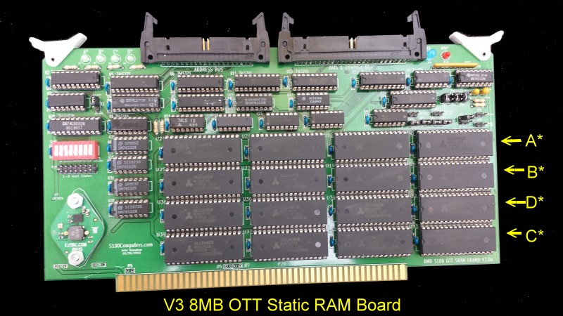
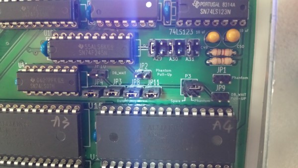
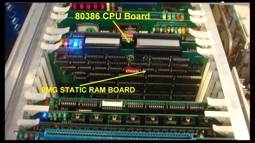
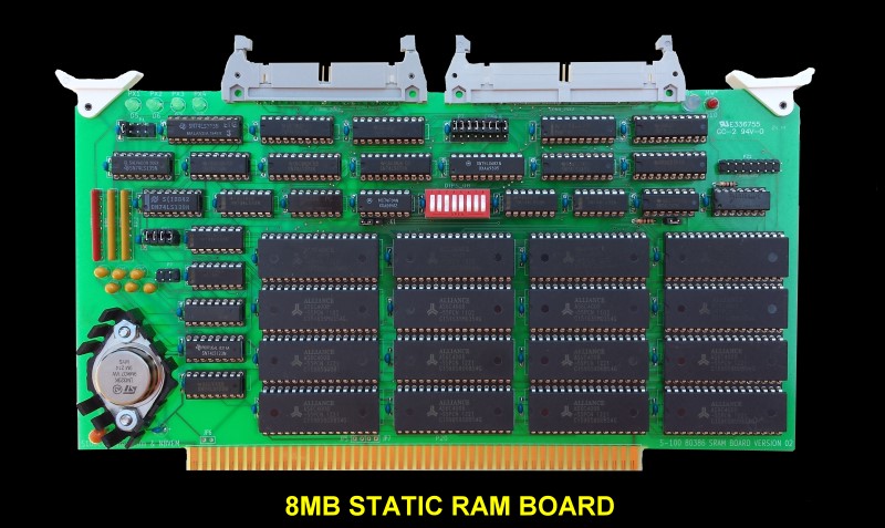
A31,30,29,28,27,26,25,24,23,22,21,20,19,18,17,16,15,14,13,12,11,10, 9, 8, 7, 6, 5, 4, 3, 2, 1, 0
  0  0  0  0  0  0  0  1  0 
0  0  x  x  x  x  x  x  x  x  x  x  x  x  x  x  x  x  x  x  x  x  x
  0  0  0  0  0  0  0  1  0 
0  1 
x  x  x  x  x  x  x  x  x  x  x  x  x  x  x  x  x  x  x  x  x
  0  0  0  0  0  0  0  1  0  1  0 
x  x  x  x  x  x  x  x  x  x  x  x  x  x  x  x  x  x  x  x  x
  0  0  0  0  0  0  0  1  0 
1  1 
x  x  x  x  x  x  x  x  x  x  x  x  x  x  x  x  x  x  x  x  x
   

From the above we see that for address lines A21 & A22 and lower, the 74LS139 (a 2 line to 4 line MUX)  handles the 4 banks of RAM.   Address lines A23 to A29 go directly to the 74LS682 as does one output of U14A (another 74LS139).  All switch settings on SW2 are grounded except the one to pin 5 of U20 (corresponding to A24).  This allows pin 19 of U20 to select all RAM on the board. With this configuration the range of RAM will be from 1,000,000H to 1,7FF,FFFH (4MB).  The four jumpers on P1 each select a 1 GB addressing range. Normally we will place this RAM board in the CPU's first GB range so we jumper P1, 1-2.

Study this table well. Hint, if A23 were also 1, RAM would start at the 16MB (1,800,000H) boundary. Remember address lines A2 to A20 are always within the RAM chips themselves (512K per chip). Address lines A1 & A0 are handled by the BE0*-BE3* signals for each of the four columns of chips.
 
There is a wait state generator on the above RAM board for slow RAM chips (U1 & jumper P23).  On this board however I am using Alliance Memory Inc. ASC4008 (512X8) static RAM chips (Jameco# 1927617,  Mouser# 913-AS6C4008-55PCN) which have an access time of 55ns.  Using a 32MHz clock on the CPU board I can run this board with no wait states.  This is important because it allows the 80386 to be run in "pipeline mode". This is a special mode where the CPU (with latched addressed hardware) can start "preparing" the next RAM address during its current cycle. This allows faster RAM processing overall.

However you may find if you use the board in the S-100 bus extender card with a long ribbon cable connection to the CPU in the bus you may need to add 1 or 2 wait states.

Finally,  remember because the 80386 has memory management hardware on board, you don't need contiguous RAM blocks.  It's fine to run the board with just enough RAM on the S-100 bus for say CPM-86 or MS-DOS and utilize the high speed off S-100 bus RAM for your application.

A V3 8MB S100-OTT Static RAM Board.
The above 8 MB OTT RAM board expected the 80386/80486 CPU boards to provide the raw CPU M/IO*,W/R* and D/C* signals (as did in the first version of our 80386 CPU board).   The more recent 80386 and 80486 CPU boards however decode the RAM Read & Write signals on the CPU board itself and send "EXTENDED_RD* and EXTENDED_WR* signals directly to to OTT RAM boards.  This provides a cleaner RD/WR signal to these RAM boards allowing for higher speed 32 bit access and reliability.  This was done on our recent (4 layer) V3 32/64 MB OTT RAM board.  

I wanted to do the same thing for this 8MB OTT RAM board.   The circuit was also cleaned up a little,  making for faster RAM RD/WR strobe signals.  Here is the core RAM select circuit:-
 
  V3 RAM Decoding

Again I went to a 4 layer board with wide traces on the critical lines.

This is an expensive RAM board. There are 16 (512K X 8 Byte) static RAM chips on the board (~$4.50/chip).   However the board has the advantage that there is no required soldering on SMD chips -- as we have on our 32/64MB OTT RAM board.  Here is a picture of the V3 Board.
  
  V3 RAM Board
  
Assembly is essentially the same as for the original board and most of the components can be directly transferred across. 
The normal jumper positions are shown here:-
  
  Jumpers

Normally this board requires no on-board wait states (P21), with our 80486 or V2 80386 CPU boards.
With all SW1 dip switches closed except position 3 (from the LHS),  the RAM will begin at Address 1000000H to 17F0000H.   
You can start with a set of only 4 RAM chips in row A* for RAM addresses 1000000-11FFFFH.

Bugs.

No bugs have been noted to date.
Please use 74F373, 74F245 and 74S32 chips as noted in the schematic.  The board silk screen list them as 74LSxxx parts.
  
  
A Production S-100 Board
Realizing that a number of people might want to utilize a board like this together with a group of people on the  Google Groups S100Computers Forum, "group purchases" are made from time to time. Please see here for more information.

The links below will contain the most recent schematic of this board.
Note, it may change over time and some IC part or pin numbers may not correlate exactly with the text in the article above.

V2 8MB STATIC RAM DAUGHTER BOARD SCHEMATIC       (V2 Final, 8/18/2014)
V2 8MB STATIC RAM DAUGHTER  BOARD LAYOUT             (V2 Final   8/18/2014)
V2 8MB OTT STATIC RAM BOARD KICAD FILES                     (V2 Final   11/11/2016)


V3  8 MB OTT STATIC RAM BOARD SCHEMATIC                     (V3 Final, 11/11/2016)
V3  8 MB OTT STATIC RAM BOARD LAYOUT                               (V3 Final, 11/11/2016)
V3  8 MB OTT STATIC RAM BOARD BOM                         
   (11/14/2016    Supplied by Rick Bromagem)
V3  8MB OTT STATIC RAM BOARD KICAD FILES                    (V3 Final   11/11/2016)

V3  8 MB OTT STATIC RAM BOARD GERBER FILES                  (V3 Final   11/11/2016)


Other pages describing my S-100 hardware and software.
Please click here to continue...

This page was last modified on 11/30/2017