The S-100 Bus FPGA Z80 SBC Board.| | 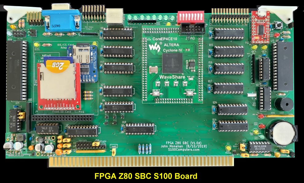 |
Introduction
The original S100 bus FPGA board has proven to be a very useful development board. The board can be morphed into many functions. If you are not familiar with that board it is essential you read up on that board before going any further here. Much of what is written here assumes you are familiar with the "V1" board. There also is an introduction to FPGAs and how to program and use them.
That "V1" board was followed up with a more generalized "V2" FPGA Prototype board which allows the user the experiment with simple FPGA circuits within the S100 bus.
We will now (again), move things up a notch and use the full power of the Cyclone IV FPGA. We will construct and program the FPGA to be a S100 Bus Z80 CPU board. The board will act as a fully self contained S100 bus "Single Board Computer (SBC), somewhat similar to our earlier S100 bus SBC's (see here and here) -- but much more powerful.
The board contains:-
A 50MHz Z80 CPU FPGA module
An 80X40 line VGA character terminal with its own ROM character table and 4K graphics RAM
An FPGA internal two page (4K+4K) ROM containing the Z80 monitor along with diagnostics support for the IDE/CF and SD cards.
An IBM PC PS2 keyboard input port (with input converted to standard ASCII)
A USB serial I/O port at speeds up to 38K to a PC
An SPI or I2C external connector interface
An interrupt controller for S100 bus interrupts.
Two SD Card slots & an interface to R/W to the two cards
One IDE CF card to run our "out of the box CPM3" (exactly like out original Z80 SBC)
A Parallel printer port with Strobe/Ack etc.
An 8 bit IOBYTE input port and 8 status LEDs.
A buzzer
There is an FPGA interface to the onboard clock/calendar RTC chip with battery backup.
The board has 512K of onboard RAM that is page addressable to the Z80
There are numerous diagnostic LEDs all around the board for debugging etc.
We use a marvelous piece of FPGA software written by Grant Searle that emulates a complete Z80 CPU in FPGA code. This on-board CPU running at up to 50 MHz FPGA Z80 does all the heavy lifting. There is no real Z80 or ROM chip on the board.!
While the board internally is quite complex, externally it looks and behaves very simple. It will be an ideal board for somebody new getting into building an S100 bus system since with this board alone and a simple USB/FPGA programmer they can have a complete CPM3 system. Then gradually the user can inactivate various sections within the FPGA code and activate the corresponding old/new S100 boards they have in their system. They can start off looking upon the FPGA as a black box. In fact to get started you don't even need an S100 bus -- just hookup 8V to a jumper on the board and connect the onboard USB port to you PC system to act as a TTY character terminal
Keeping in mind the above potential audience, I will try and over-explain some things below. Our "hard core" audience can just skip ahead. That said this is NOT a board for a complete electronic novice. Minimally you should have some soldering experience and knowledge of electronic circuits. You should for example be comfortable with web sites that describe Arduino or Raspberry circuits. You should have a basic understanding what a Field Programmable Gated Array (FPGA) is. If not, look them up on web. In summary, these chips allow you to lay down any circuit you might come up with within the chip just like you might do by soldering hundreds of TTL/74xxx chips together as in the old days. Its all done in software. The resulting code/pattern is then programmed into the chip.
What Is Needed
The FPGA we will use here is an Altera/Intel Cyclone IV FPGA. This chip is currently in about the middle range of the programming capacity of FPGA's. The actual chip uses a "Ball Grid Array" method of soldering it to a printed circuit board. This requires very specialized equipment, so normally one purchases an "adaptor board" for these chips with the chip on it. Besides providing "normal" pin attachments to (in our case), the main S100 board, these adaptors contain a number of voltage regulators, Flash RAM, a programming socket and other components these FPGAs require to operate.
As for our previous boards we will use the WaveShare "CoreEPCE10" Cyclone IV board adaptor. Its schematic can be seen here.
The second thing you will need is a device to program the FPGA chip itself.
There are many FPGA programmers available. I really like the USB Blaster (V2) that Waveshare sells. Its simple and reliable. And importantly, works directly within Intel's Quartus V12 (see below). The good news is; With this board you will not need to purchase a separate EEPROM burner, GAL programmer or CPLD programmer.
Somewhat unexpectedly you will need to pay particular attention to the special very tightly spaced pins on the above adaptor board. Because there are so many FPGA output pins, its not practical to have a connector with the standard PC board 0.1" pin spacing. The above WaveShare unit uses unusual 2 mm dual row pin connectors. Unlike to normal 0.1" connectors these are quite rare an expensive. If you solder these female sockets to the board the WaveShare adaptor sits quite high on the board and will prevent the next S100 bus slot from being used. If you carefully remove the JTAG socket top border edge with a wire cutter - all around about 1/8 ", it will fit into most S100 bus motherboards without taking up two slots. Alternatively you can solder the adaptor directly to the S100 board. Of course removing the adaptor is all but impossible in this case.
Please note the 2 mm dual row pin connectors (Digi-Key #S5750-30-ND sockets) for the WaveShare adaptor are quite tricky to fit on to the board. I found the best way to do this (after trimming to size), is to push them half way on to the adaptor pins and then wiggle them to fit the whole unit on to the S100 board. Figure on spending 10 minutes on this step! Do not solder them to the board first and then try and press the adaptor down on them. They are very fragile and internally the leaves will bend if socket angles are not exactly correct. When in place, check each pin is visible on the back of the board before soldering. Only then solder all around. Add as little solder to each pin as possible - the narrow pins have a tendency to wick up solder internally.
Leonard Young recently pointed out better sockets are available from Mouser (Preci-dip 833-87-038-10-001101) as part 437-8338703810001101 for $3.04 ea. You’ll need a few, since 38 positions is a 2x19 strip. To cut to size. Clip with a wire cutter one pin past that required pins and then file down to size. Recently I noticed that DigiKey sell better 2X50 pin sockets (Part #1212-1786-ND).
The rest of the boards components are standard -- available from Jameco, Mouser, Digi-Key etc. For prototype boards I generally use "double swipe" IC sockets. For a critical board like this I prefer to use "Machine Tooled" IC sockets. However they are more expensive and you have to be particularly careful not to bend the actual IC pins.
Programming the Cyclone IV FPGA
As mentioned above, in order to actually implement a circuit the FPGA must be programmed. During board development the code is passed to a Flash RAM on our adaptor board from which the FPGA has enough intelligence to load it from there and run. This means that if we power down the board that code is lost and the chip has to be re-programmed. As we shall see below. when one is satisfied with the code there is a separate process to burn it into the chip so it is not lost upon power up. This is a slower process and so is not normally done. You can however program by both methods essentially an infinite number of times.
There are two major languages to program FPGA's Verilog and VHDL.
Verilog was created by Prabhu Goel, Phil Moorby, Chi-Lai Huang and Douglas Warmke around 1984. Originally, Verilog was only intended to describe and allow chip hardware simulation. The automated synthesis of subsets of the language to physically realizable gates etc. was developed after the language had achieved widespread usage. Verilog stands for the words "verification" and "logic". There were many upgrades/extensions over the years. The last major version appeared in 2005.
VHDL was originally developed for the U.S Department of Defense in order to document the behavior of the ASIC chips that supplier companies were including in equipment. Because of this background much of the syntax was based on the Ada programming language. The language has undergone numerous revisions and has a variety of sub-standards associated with it that augment or extend it in many ways, the last major release being in 2008.
Usage between the two tends to be polarized. Probably because of its Ada/Pascal style VHDL seems to be more popular in Europe. The "C'" style syntax Verilog seems to be more popular in the US.
With both the above languages you can write programs line by line just like is C or Java etc. Alternatively you can use a newer graphic diagram approach which in the background converts your graphic diagrams into Verilog of VHDL code -- totally transparent to the user. This approach uses a special file called a "Block Diagram File" (.bdf) (for Altera/Intel chips). The whole process is somewhat like writing a web site page. You can either write the whole page yourself in HTML or use something like I'm using here (Expression Web), to "draw" a web page in blocks, graphics etc.
Again, usage between the two approaches by people tends to be polarized. The good news is that within IDE's you can import and export modules for both types. You can for example see/export the Verilog code that makes up a complex .bdf module or you can convert a Verilog module into a .bdf module.
Coming from by now, years of experience using KiCAD to lay out over 100's of S100 bus PC boards I personally found the .bdf approach of programming an FPGA very easy. Within a day or two I was up and running programming an FPGA with quite complex circuits. This was possible because the Quartus IDE (see below), supplies libraries for things like all the common 74xx logic chips, many of the common VSLI style chips (e.g.. UARTs) etc. It contains many libraries of many extremely complex/useful modules such as CPUs. While you can drill down for detail, at a top level they behave as "black boxes". You just supply the wire or bus connections -- which you draw as lines. It would take me months of learning to do the equivalent in raw Verilog code. I will illustrate this below.
BTW, there is one well known/subscribed source code site for FPGA's called OpenCores where you will find an enormous list of FPGA projects/code. There numerous other excellent FPGA code applications on the web. For example Javier Valcare's FPGA home page and fpga4fun.
Quartus Prime.
For Altera/Intel FPGA's the program of choice to program them is called Quartus Prime. This a very large Windows based IDE interface. It is completely self contained with everything you need to write FPGA code and program the chips. Its an expensive software package. Fortunately Intel supplies a "Quartus Lite" free version for students and people like us. Even this is way overkill for our use. The most recent version can be downloaded from this Intel site. The package will take ~20 minutes to install on Windows 10. You may want to first review this video about the installing process. Please see the Notes section at the bottom of this page for more help installing Quartus.
Please keep in mind that programming an FPGA is different from the normal linear/sequential programming approach you may be used to. On an FPGA everything is potentially happening at once. Good FPGA programmers take years to excel and currently are in high demand. Timing and power distributions across the chip almost become an art form. Fortunately out needs will be far simpler. Also there seems to be an excellent community of experienced people ready to help -- beginners. I have found the Altera forum to be very useful and helpful. However by far the best way to get started is to look at a few YouTube demonstrations.
One outstanding YouTube video to get you going with Block Design File FPGA programming is this one by ClockFabrick Electronics Academy.
A text summary is provided here. If you cannot get to that YouTube video you can directly view it in the video below.
Note, click on the "full screen icon" for easy viewing. Use ESC to return.
Also please allow a few minutes for it to download. It's a very large (50 minutes) video file.
For absolute FPGA beginners, rest assured, you can more or less use the FPGA code examples below as "Black boxes" to get this board up and running. However you will be missing one major aspect of the board. By stepping along and understanding how the FPGA code works you will in the end have the ability to modify the board in amazing ways -- up to the point of even using a different CPU.
Before we start, a few things about our FPGA code file directory structures. We will "build" our FPGA code in steps of increasing complexity. I have found out the hard way, that that you have to be very careful with Quartus where you place your files. The actual Quartus "Project file" work Z80_FPGA.qpf should reside in the main folder you will build your programs. In my case it happens to have a path:-
C:\intelFPGA_lite\18.0\quartus\MyFPGAPrograms\Z80_FPGA\Z80_FPGA.qpf
The above path (in yellow) is the root below which we will build all files in this project. Your path may be different but the Z80_FPGA directory must exist.
The actual Z80_FPGA.bdf in this directory is our current "work file" which when compiled we use to program the FPGA.
You will notice in the download (see bottom of this page) , numerous Z80_FPGA1.bdf, Z80_FPGA2.bdf , FPGA3.bdf...... files. these are the main Z80_FPGA.bdf file of increasing complexity as we add FPGA components/modules to our board. The file Z80_FPGA.bdf is always the most sophisticated and current file constructed. It will get more complex over time.
In every case as we build, we first "Close" the current Z80_FPGA.bdf file it within Quartus. Note not the project file (Z80_FPGA.qpf).
We then go outside of Quartus into windows and delete (or rename) it.
We then take the next more complicated Z80_FPGAx.bdf file (Z80_FPGAx+1.bdf) and rename it Z80_FPGA.bdf
We then go back to Quartus and open this Z80_FPGA.bdf file and work on it.
The key thing here is Quartus does not know we switched files on it. This way all pin designations, ROM and RAM preloaded .HEX files remained unchanged. Plus other things. If you start flipping files around renaming them etc., within Quartus it gets confused -- without telling you.
I cannot stress enough the trick of saving old .bdf files, renaming them etc. along the way. This way you can easily fall back to the last good working example. Saved my neck many times!
A few things about Quartus.
1. It constructs a number of sub-directories as it constructs its FPGA code below the Z80_FPGA. You don't have to bother about them.
2. As Quartus compiles your code, it seems to send out endless information in messages. Again don't bother about them unless it tells you (in red text) that there are errors at the end.
3. Be very careful when you place copies of a logic item. Sometimes when you click you can place one item exactly over another yet the item appears as only one unit. For example a NOT or a NOR gate. The compiler will insist the gate has no input when in fact there is a hidden gate under it.
4. Be careful when you join up and input or output port to a wire or bus line. Make sure they join by dragging them apart.
5. Some gates are negative true. I use names like pWR- to signify this. Quartus does not accept pWR*.
6. Be sure you assign actual pin numbers to FPGA inputs and outputs. Quartus does not tell you if they are unassigned.
7. As I said above build a circuit in stages of increasing complexity saving versions along the way.
8. Be sure the designated FPGA for a new project is a EP4CE10F17C8 FPGA for the above WebShare board.
BTW, the actual compiling and programming process takes longer than you might expect (~3minutes for the complete program).
Installing Quartus Lite on Windows.
In spite of its name the Quartus Lite IDE is a large program. When fully installed the Quartus folder is over 15GB in size. Installing it makes Microsoft's Visual Studio seem lightening fast!
That said, its an excellent IDE. Figure on 1 hour to install and get it right. For our purposes we will only be using probably 5% of its capabilities, but I have found if you try and get smart by not downloading or removing sections you run into problems later during usage.
Please see here for instructions on how to install Quartus.
Location of the Monitor .HEX Files
All the examples below count on the FPGA Z80 reading its ROM module and it being in an Intel .HEX file format. I supply the full .HEX files at the bottom of this page.
It is essential that Quartus can find the relevant .HEX file during the compile. There are numerous examples below of .brd files of increasing complexity.
Before a compile right click on the 4K, 8K or 16K FPGA ROM module, select the IP Parameter Editor, and click Next twice, the path for the .HEX file is displayed.
Check you actually have the .HEX file at that location. If not, browse to the correct location.
Late I will describe how you make your own Z80 monitor HEX file.
As we will see, we can have three different size ROMs in the Quartus .brd file. We will start off with a simple monitor in a 4K "ROM". This will contain all the common Z80 monitor commands you are used to.
Later when we add more code for Xmodem and IDE/CF card interface we will increase the "ROM" to 8K. Still later we will increase the "ROM" to 16K to
accommodate an SD card drive menu.
Now we don't want to have a 16K block or ROM eating up our RAM space when using CPM etc. so we
actually use only one 4K block or ROM at a time "paging" each in, in hardware at F000H to FFFFH.
Initially you will see a 4K ROM in the .brd files, later an 8K one and still later a 16K ROM. They all behave the same way. The trick is how you get the .HEX file code into the correct areas of the ROM.
I will describe this later below. For now, just remember that all ROM code .HEX files must reside in a location the Quartus ROM module can find.
They may be assembled
elsewhere on your system but the .HEX files must be placed in that correct folder for Quartus to see them.
Step By Step Building the FPGA Z80 SBC Board.
The build instructions are fairly simple for this board but because it is a complex board building it should not be rushed. As always, first examine the bare board carefully for scratches or damaged traces, use a magnifying glass if need be. A broken trace is almost impossible to detect by eye on a completed board.
Solder in all the required IC sockets, resistors, resistor arrays, capacitors, jumpers, and the Pololu 5V and 3.3V (LM3940) voltage regulators. Also do not add the MicroSD Card Adaptor or RTC crystal yet. Please be sure you put the resistor arrays in with the correct orientation of pin 1. An incorrect orientation is one of the most difficult things to detect/debug on a board if not noticed. Check their values before soldering (they are difficult to remove). Insert all jumper arrays. Note there are two sockets for the Pololu 5V regulator. While the older ones (D24V25F5) are still available, it seems Pololu is suggesting users use the D24V22F5's (5V, 2.5 Amp) units. Unfortunately the plated-through holes for P2,P3 and P4 are a little too small for the Pololu pins they supply with the regulators. You can either use a single row socket on the board and then use the Pololu pins, or file them slightly front and back and force them in using the side of a blade, pressing down on them. When in place only then solder the actual regulator to them.
When adding the LED's be sure to orient them correctly. (Usually the longer lead in the square pad). For the buzzer (SP1) the + side is toward the outer edge of the board.
Please take care to not "slobber" solder on the sockets. They are very closely spaced on this board with vias often close to a socket pin - particularly for the FPGA adaptor sockets.
For prototype boards I generally use "double swipe" IC sockets. For a critical board like this I prefer to use "Machine Tooled" IC sockets. However they are more expensive and you have to be particularly careful not to bend the IC pins. Solder in the buzzer SP1 with the "+" pin on the RHS. You may wish to play around with the buzzer sound volume by replacing the 100 Ohm resistor R11 with a lower one say 75 Ohms or 33 Ohms to get a louder buzzer sound later. So solder it high on the board for easy removal.
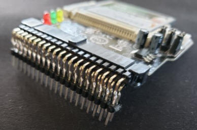
Here is a picture of the board at this stage (With the WaveShare FPGA Inserted):-
For testing remove every S100 bus board in your system except (if you have one, the S100 Bus SMB and/or the Bus Display Board). If you have neither of these boards you must press the reset button (SW2) on the board itself to run the actual FPGA program (after uploading it). As we shall see below during the software build, there are two options for the Z80 monitor console IO. If you have a Propeller Console IO Board, great, use it. If not, you will need to use the onboard USB port connected to a TTY terminal on your PC for monitor IO. The former option is much better and far easier to get going. It will be a few steps down before you have a working USP port. Except for looking with a logic probe at critical signals you will be in a sense flying blind in that case.
Lets get started, Place the board as shown above in the bus without any chips inserted, (including the Waveshare FPGA adaptor). There are two separate voltage rails on this board 5V and 3.3V. Carefully examine the schematic and check the voltage to the individual sockets are either 5V or 3.3V. Be sure you have 3.3V and 5V going to the appropriate pins on the Waveshare FPGA adaptor socket.
If you are comfortable with the above, carefully insert the WaveShare Cyclone IV adaptor in its sockets. Power on the computer. "Virgin" Cyclone IV Adaptor boards from WaveShare seem to have the FPGA preloaded with a program (in the EPCS16 Flash RAM) that already that pulses its 4 onboard LEDs. Note the flashing rate.
Within the Quartus FPGA project folder (the expanded FPGA Z80 (V1.1) - FPGA Z80.zip, see below), erase Z80_FPGA.bdf and copy Z80_FPGA0.bdf to Z80_FPGA.bdf.
Please note the actual Z80_FPGA.bdf file in the above FPGA Z80 (V1.1) - FPGA Z80.zip download is the final (Step 16 or later steps, see below) FPGA code.
It is there only for experts that have used Quartus and know how to code FPGA's using .bdf files.
Everybody else should delete it and step things along (Z80_FPGA0.bdf ,1,2...15) as described below.
Let's get started...
Go to your C:\intelFPGA_lite\18.0\quartus\MyFPGAPrograms\Z80_FPGA\
Directory. Delete the file
Z80_FPGA.bdf
Copy the file
Z80_FPGA0 -- (LED's TEST).bdf to a file Z80_FPGA.bdf
Then go back to Quartus and open this Z80_FPGA.bdf file and work on it
as follows.
Load Quartus and open the Project file Z80_FPGA.qpf, then open the file Z80_FPGA.bdf. When loaded, "Compile the Design", then "Program the Device" and then hit the "Start" button.
The LED's on the Waveshare adaptor should flash differently. To confirm, kill the power and reboot the computer. The code in the FPGA is lost so the original flashing rates should reappear.
Note, if you are using a previously programmed FPGA adaptor with code "burnt" into the FPGA the power-on flashing will probably not be present.
In fact, Waveshare may in the future supply adaptors without the flashing code in them. Here are some pictures:-
Very important the LED D10 "BOARD_ACTIVE" should be flashing.
This is your first connection of the FPGA adaptor to the outside world! Do not go forward until you see this response.
1. The address line test.
First add U8, U10, U14, U15 &, U16. Add JP1 & JP2.
We will next load a simple FPGA program to test our S100 bus address lines connection to the bus.
Within Quartus, close the current Z80_FPGA.bdf file. Note, not the project file (Z80_FPGA.qpf).
Then go outside of Quartus and into windows and delete (or rename) it.
Then take the next more complicated file, Z80_FPGA1
-- (Address Lines Test).bdf, and copy it to a file Z80_FPGA.bdf
Then go back to Quartus and open this Z80_FPGA.bdf file and work on it.
First look it over carefully to understand what is happening. It's in essence just a 16 bit counter increasing the S100 bus address lines.
Here is a picture of part of the core module.
You see we also pulse the pSYNC, pSTVL, and pDBIN. This is because the S100 Bus SMB and/or the Bus Display Board do not display the actual S100 bus address lines unless they are latched into the LED displays by these signals. Do not get too hung up on the accuracy of this circuit its just a quick and dirty emulator for Z80/S100 bus signals.
That said, the address lines on the bus should be continuously changing. If not check the signals going to (3.3V) and coming from the 74LVC245's U8 & U10 as well as the Address line buffers U14, U15 & U16.
2. The address Line Test Using the Z80 FPGA Core CPU.
Next we will do the exact same thing using our "real" Z80 to increase the address lines. For the Z80, an input of the opcode 00H on its data lines will do nothing. The CPU just goes to the next higher address. So if you ground the 8 data lines of a Z80, after a reset it will read in the 8 data lines at address 0000H. See its a nop and do the same for 0001H. It will continue to do this all the way up to FFFFH and then roll-over to 0000H again. This is in effect what we have in our Z80_FPGA2.bdf file. So as before...
Within Quartus, close the current Z80_FPGA.bdf file. Note, not the project file (Z80_FPGA.qpf).
Then go outside of Quartus and into windows and delete (or rename) it.
Then take the next more complicated file Z80_FPGA2
-- (Address Lines Test with Z80).bdf, and copy it to
a file
Z80_FPGA.bdf
Then go back to Quartus and open this Z80_FPGA.bdf file and work on it.
Add U9 and U11.
Again, look it over carefully to understand what is happening. It's in essence using the Z80 module as a 16 bit counter to increase the S100 bus address lines. Here is a picture of part of the core module.
You should see the address lines increase from 0000H after hitting the reset button SW2.
Also the increase should stop if you push the RDY or XRDY button on the SMB.
Don't get too hung up on how the S100 bus signals are generated. It's a "kludge" to fool the SMB or Bus Display board to latch the address lines.
3. Adding a FPGA ROM to the Z80 Core CPU.
First add U4, U12, U17, U13.
We will now add some intelligence to the Z80. We will hook to its data in lines a ROM module programmed within the FPGA.
Within Quartus, close the current Z80_FPGA.bdf file. Note, not the project file (Z80_FPGA.qpf).
Then go outside of Quartus and into windows and delete (or rename) it.
Then take the next more complicated Z80_FPGA3
-- (Output 3's to port 01H).bdf
file and copy it to a file Z80_FPGA.bdf
Then go back to Quartus and open this Z80_FPGA.bdf file and work on it.
Look it over carefully to understand what is happening.
The actual ROM module is obtained from one of the Quartus IP libraries.
We will start off with an 8K ROM.
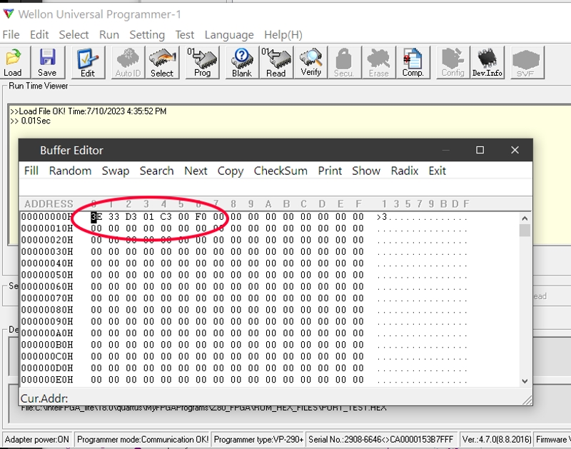
The Z80 will start off as before reading in 0's on its data in lines until the address F000H is reached. At this time the ROM's OE* "pin" is activated and the Z80 starts reading the ROM at address F000H. The ROM has the following simple code:-
START: LD A,33H
OUT 01H,A
JP START
in actual bytes this would be:-
3E,33H,D3,01,C3,00,F0
After a few seconds delay this will output continuously 3's on the Console IO port.
If you are using the USB port only and a PC connection, sorry, you will only see pin 17 of U8 pulse with a logic probe.
Its important to appreciate that while the code runs at F000H within the Z80's address space the actual
ROM code must start at 0H within the ROM.
Quartus expects an "Intel" HEX file format for ROM code. Simple code like the above can actually be entered by hand using most ROM programmers software.
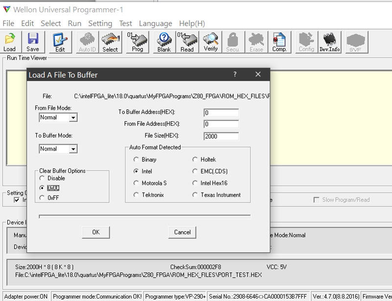
You can for example download the software for a Wellon VP299 (or later) Programmer from here:-
http://www.weilei.com/dow.asp
and install it. You do not need hardware to run it. Select
a common ROM such as a 28C64 ROM from the menu.
Here is a picture of the
three relevant steps to make a "PORT_TEST.HEX" file for use with Quartus.
The file is actually supplied below, but you need to know how to make Quartus .HEX compatible files.
The PORT_TEST.HEX file
(located at
C:\intelFPGA_lite\18.0\quartus\MyFPGAPrograms\Z80_FPGA\ROM_HEX_FILES)
must reside in the FPGA ROM starting at the ROM's 0H location.
Here is the step by stem process
| |
 |
| |
Load the PORTS_TEST.HEX file
|
| |
 |
| |
Examine the start of the HEX file
|
| |
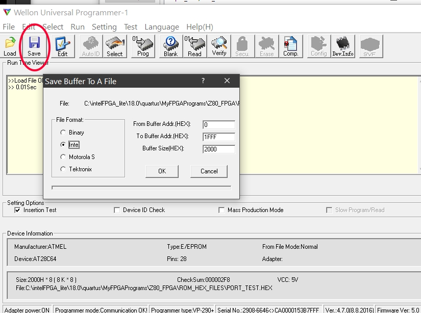 |
| |
Write the .HEX file to the directory
...\Z80_FPGA\ROM_HEX_FILES\
|
It's very important you select the Intel File format and the buffer address starts at 0H
Next we need to insert an actual
"real" code containing FPGA software ROM module.
In our application we will use a simple 8 bit, 8K ROM
here. Way overkill here, but we will use most of it later.
We will position the ROM in the Z80_FPGA.bdf file to start at F000H.
We need to load the above .HEX file into this ROM within Quartus.
Generally the ROM .HEX files are made/stored in a folder outside the main Quartus folders. You need to point Quartus to them.
In all the cases below the ROM HEX files are stored in the folder:
...\Z80_FPGA\ROM_HEX_FILES\
The good news is that once you define the .HEX file path and name, Quartus will always find it for subsequent FPGA builds.
You don't have to reload them each time into the ROM module IF you did not change it's name
Let's look at our FPGA code "hardware"
The FPGA coded 74682 goes low when the Z80 reaches address F000H.
This triggers the Flip-flop (FF) JMP_ENABLE low so the address lines are no longer grounded. It also enables the FPGA ROM and the tri-state buffer from its data lines so the ROM now supplies data to the Z80. From it code to continuously send 3's to the Propeller Console Data out port is sent. You should see something like this on your console.
Note it takes about 1 second for the '3's to start to appear because we are using a very slow CPU clock at this stage.
You must get this FPGA program working before going any further.
If you don't have a Propeller Console IO board be sure you see U4 pin 19 is low and U8 pin 17 is pulsing with a logic probe.
4. Adding the Z80 to S100 Bus Port Interface
The above step simply used the raw write signals from the Z80 module. We need to very carefully modify them so that they generate the corresponding signals of the S100 bus as specified in the IEEE-696 S100 bus specifications. Only then can we be sure the board will work with other S100 bus boards.
The FPGA circuit we use to do this is a direct copy of that on our Z80 SBC (and the original Z80 board).
These boards are very reliable the latter now being over 10 years old.
Unfortunately the actual circuit is a little complex. It's actually a close copy
of the Intersystem's
Z80 II CPU IEEE-696 board. Most users can look upon the circuit as a "black box". Z80 signals go in, S100 bus signals come out.
Within Quartus, close the current Z80_FPGA.bdf file. Note, not the project file (Z80_FPGA.qpf).
Then go outside of Quartus and into windows and delete (or rename) it.
Then take the next more complicated Z80_FPGA4
-- (S100 Bus Core Added).bdf file and copy it top a file
Z80_FPGA.bdf
Then go back to Quartus and open this Z80_FPGA.bdf file and work on it.
Again, look it over carefully to understand what is happening. In essence its a repeat of the previous version except now we send out "proper" S100 bus signals.
Here is a picture of the main Z80->S100 bus conversion module.
You should see the exact same 3's output on your Propeller Console IO board. Or for USB port users, pulses on U8 pin 17.
Please remember at this point we have a bare bones S100 bus interface. Sometimes the Z80 takes time to lock on to the F000/ROM address. It can take a few seconds. You can try changing the clock input from 2mHz to 4mHz or 10mHz
if you like.
5. Adding an Input Port IO to the Z80_FPGA Board.
Next we will check Input from a port. Add U7.
Even though we will not need it until the next step, add the RAM chip U5 (a AS6C4008, 512X8 SRAM chip) to stabilize the address/data lines, and jumper JP7
We will modify the above "PORT_TEST.HEX file to the following:-
ROM has the following simple code:-
START: LD A,33H ;Display '3'
START2:OUT (01H),A
IN A,(01H) ;Get a keyboard character
JP START2
in actual bytes this would be:-
3E,33H,D3,01,DB,01,C3,02,F0
We will call this PORT_TEST2.HEX. Load it into the FPGA ROM exactly as described above. i.e.
Within Quartus, close the current Z80_FPGA.bdf file. Note, not the project file ((Z80_FPGA.qpff).
Then go outside of Quartus and into windows and delete (or rename) it..
Then take the next more complicated Z80_FPGA5
-- (Input from a port).bdf file and
copy it to a file Z80_FPGA.bdff
Then go back to Quartus and open this Z80_FPGA.bdf file and work on it..
Compile and run the Z80_FPGA.bdf file.
Press a keyboard character. You should see it displayed on the Console. Again USB port users should look for pulses on U8 pin 17.
You must get this program working before going further.
6. Adding RAM to the Z80_FPGA Board.
Next we need to activate RAM access to our Z80 module. This is where things get a little tricky. First you will notice that the Z80 FPGA module as written, has a separate 8 bit data in and a separate 8 bit data out bus. This makes things very convenient to interface with the S100 bus which also has separate in and out data lines. We will however be using a "real' RAM chip on this board (AS6C4008, 512X8 SRAM chip). Like all such RAM chips, the data lines are bidirectional. We need to accommodate this within our FPGA for Z80 RAM access. We do this with the following FPGA circuit. We handle each of the 8 RAM data bits with the following circuit.
Eight of the dual tri-state buffers are used with the FPGA pins that directly interface the RAM chip (U5). Note the RAM chip itself has a VCC of 3.3 Volts. (This chip will work at 5 or 3.3 Volts). The OE* and WR* signals from the FPGA are also 3.3 volts. Most important the address lines are 3.3V coming directly from the FPGA. This as we will see later allows us to run a very fast clock for the Z80 module itself
A second complication is that data to the Z80 may come from circuits on the Z80_FPGA board itself or from the S100 bus. Again we must accommodate this within the FPGA. Since the Z80 has separate in and out data lines this simplifies things. For data out its simple, the data can go to both locations (s100 bus or the FPGA "circuits" on the board), the Z80 control and status lines within the FPGA define which are relevant.
For data in however we must control which 8 bits actually reach the Z80. We use the following circuit:-
Basically we will assume any Z80 data input comes from the S100 bus unless told otherwise. In the above, for now, ANY Z80 input from an I/O port..
As we developed our FPGA circuits below we will add exceptions to this by supplying negative signals to the 8 input AND gate. (Remember
Highs activate the tri-state buffers)..
Within Quartus, close the current Z80_FPGA.bdf file. Note, not the project file ((Z80_FPGA.qpff)..
Then go outside of Quartus and into windows and delete (or rename) it..
Then take the next more complicated Z80_FPGA6
-- (Added RAM chip).bdf file and copy it to a file
Z80_FPGA.bdff
Then go back to Quartus and open this Z80_FPGA.bdf file and work on it..
To test our new addition we need to change the code in the FPGA ROM to a file derived from RAM_TEST.Z80 which we will call RAM_TEST_FPGA_ROM.HEX
The core of the RAM_TEST.Z80 file is:-
COLD: LD HL,RAM_BASE ;We will check we can store and change a byte at RAM location E000H
RAM_TST:
LD A,'@' ;For quick hardware diagnostic test
OUT (S100_CONSOL_OUT),A ;Force a "@" on the CRT if ROM access is active
LD (HL),'?' ;Default 3FH
LD B,0FH ;Count 16 times
PROP_CI1:
IN A,(S100_CONSOL_STATUS) ;Get a character
AND 02H
JR Z,PROP_CI1 ;Wait until something there
IN A,(S100_CONSOL_IN)
AND 7FH
LD (HL),A ;Store in RAM
PROP_CSTS1:
IN A,(S100_CONSOL_STATUS)
AND 04H
JP Z,PROP_CSTS1 ;Z if not ready
LD A,(HL) ;Get stared value from RAM
OUT (S100_CONSOL_OUT),A
DJNZ PROP_CSTS1 ;Do 16 times
This time it's a little too much to do by hand. Its supplied below (as RAM_TEST.HEX), but you should know how it is done/assembled by opening up the RAM_TEST.Z80 in its own folder and generating a hex file RAM_TEST.HEX with your favorite Z80 Assembler. See here. Again as described above, while the actual code resides in the Z80's address space at F000H it must reside in the ROM at 0H.
Repeat the process described above to make 0H based .HEX file for Quartus. Do not save the file with the same name, I use RAM_TEST_FPGA_ROM.HEX. Then go to Quartus and program the FPGA ROM with the RAM_TEST_FPGA_ROM.HEX file -- again as described above.
Remember the RAM_TEST.HEX file has a starting address of F000H, the RAM_TEST_FPGA_ROM.HEX has a starting address for the ROM at 0H.
Then compile, load, and run the Z80FPGA.bdf file. Hit the system reset button. Then enter a keyboard character.
You should see that the value is not stored in RAM and will give you a display like this:-
As you can see above we are saving a byte in RAM and then reading it back from RAM and sending it to the console.
Again unfortunately if you only have a USB port console you are still flying blind just seeing U8 pin 17 pulse.
At this point you are well on your way to having a working board. You have a Z80 CPU, ROM and RAM and IO/Port addressing.
7. Adding
a ROM Monitor to the Z80_FPGA Board
Now that we have a functioning RAM and ROM we can add a "real" Z80 monitor to
the board. We will use a modification of our
general Z80 Master monitor that
we have fine tuned over the years. Here we will call this monitor
SBC-MONA.Z80. Typically
it is written, modified and assembled at another location rather than the FPGA
folder we are using here. Where does not matter. What does matter is the
final .HEX file
must always resides in our
...\Z80_FPGA\ROM_HEX_FILES\
folder.
It has to be a .HEX filed written to run at F000H but reside in the ROM at 0H.
We will describe later below how to construct and locate such a
.HEX file for Quartus and
place it in the FPGA ROM correctly to be used by Quartus.
For now just make sure your ...\Z80_FPGA\ROM_HEX_FILES\
folder contains a .HEX file named
SBC-4K-MONITOR.HEX
Within Quartus, close the current Z80_FPGA.bdf file. Note, not the project file ((Z80_FPGA.qpff).
Then go outside of Quartus and into windows and delete (or rename) it..
Then take the next more complicated Z80_FPGA7
-- (Z80 Monitor in RAM).bdf file and
copy it to a file Z80_FPGA.bdff
Then go back to Quartus and open this Z80_FPGA.bdf file and work on it..
Compile and run the Z80_FPGA.bdf file.
You should see:-
We will discuss the monitor in more detail in section 9.
Please note that at this stage not all of the menu options will work (only, A,D,E,F,G,J,K,M,Q,R,S,T,V,Z).
Here is a picture of the board at this stage:-
You are making good progress!
8. Adding the IOBYTE, Wait States & RAM Bank Selection to the Z80_FPGA Board.
On this board we assign port 36H as the IOBYTE port. This BTW is the same port we use on the Z80 SBC Board, however the use of the bits are different.
Within Quartus, close the current Z80_FPGA.bdf file. Note, not the project file (Z80_FPGA.qpf).
Then go outside of Quartus and into windows and delete (or rename) it.
Then take the next more complicated Z80_FPGA8
-- (Added Wait states, IOBYTE, RAM Pages).bdf file and copy it to a file
Z80_FPGA.bdf
Then go back to Quartus and open this Z80_FPGA.bdf file and work on it.
Here is a picture of the relevant FPGA circuit.
Most of this circuit we will not use quite yet. We only want to read the value of the 8 dip switches (SW1) addressed at port 36H.
Close one or more of the upper IOBYTE switches and reset to board. They should display correctly on the monitor Signon.
Next Display/Fill RAM at 0-100H
Output to port 36H 01H.
Again display RAM at 0-100H. It should be different. Also LED D17 (High RAM) should light up.
Output to port 36H, 00H.
The original RAM values should re-appear.
Note while the current configuration allows only two 32K pages for banked CPM (see below). The circuit can easily be modified/enlarged for more.
9. Adding the USB Port to the Z80_FPGA Board.
We will now add a USB Port for Console I/O to the board.
This will be a relief to those that do not have the Propeller Console IO Board and have been flying almost blind up to now.
This also is the first time we will be using Public Domain software modules. As I said above, these are available for chips like the Cyclone Series in many places on the web. I mention in particular OpenCores, Javier Valcare's FPGA home page and fpga4fun. In most case however the source is in VHDL or Verilog "raw" format.
Fortunately Quartus allows you to convert the module to a .bsf file so it can be used directly in our (growing) Z80_FPGA.bdf file.
In this case we use the UART.V file from OpenCores Then under the File menu:- Create\Update, Create a Symbol File from current file. We create uart.bsf.
Then within the Quartus Symbol Tool, under Project, you will find uart. Drag that into your growing .bdf file -- I always add components at the bottom.
This is how one adds software modules in Quartus. Its already loaded for you however in our next version of Z80_FPGA9
-- (Added USB Port).bdf.
So again repeating the drill:-
Within Quartus, close the current Z80_FPGA.bdf file. Note, not the project file (Z80_FPGA.qpf).
Then go outside of Quartus and into windows and delete (or rename) it.
Then take the next more complicated Z80_FPGA9
-- (Added USB Port).bdf
file and copy it to a file Z80_FPGA.bdf
Then go back to Quartus and open this Z80_FPGA.bdf file and work on it.
Here is the core circuit.
We will now add the ability to direct where Console IO data will come from and be sent to.
We do what we have always done with our S100 bus CPUs, we utilize a few bits on a read/write port that are utilized by the Z80 ROM based monitor to decide where console I/O originates.
This is an age old approach first used in S100 bus systems in the TDL SMB and its Zapple monitor.
On this board in its current final form (see below), there are 4 different I/O possibilities for a Console for the Z80 Monitor (and CPM).
1. The Propeller Console IO board.
2. A USB port connected to a PC and a TTY character terminal.
3. For both of the above, the keyboard can instead come from a PS2 keyboard connected to the boards PS2 socket P20 or P22.
(Not yet installed, see below)
4. For all 3 of the above, the Console output can instead go to a VGA display connected to the boards VGA socket J1 or P21.
(Not yet installed, see below)
The decision in the Z80 monitor is based on the lower 4 bits of the 8 bit IOBYTE port. Defined as follows.
xxxxxx11 All console IO goes via the Propeller Console I/O board.
xxxxxx10 All console IO goes via the USB port/PC TTY terminal
xxxxxx0x
Input for the console (above) is overridden and always comes from the PS2
keyboard, (Not yet added, see below).
xxxxx0xx
Output for the console (above) is overridden and always goes to the onboard VGA
display, (Not yet added see below).
So for example if the IOBYTE port is absent/ non-functioning (11111111), all Console IO will be via the Propeller Console I/O board.
If the IOBYTE port is xxxxx00x the PS2 Keyboard and VGA display would be the Console.
First add and set the dip switch SW3 to all open.
The above circuit is actually an RS232 UART circuit. We use one of the common RS232->USB adaptors to convert the bidirectional data to a USB format.
I like to use the SparkFun FT231x. It's simple and reliable and uses a USB micro connection. It can run at 5V or 3.3V. Since we are connecting the chip to the FPGA directly you need to jumper the chip on the back to 3.3V.
Sparkfun also supplies a Sparkfun FTDI "Basic" converter which uses the older USB micro connector.
Adfruit (and others) also supply similar converters -- unfortunately they are not pin for pin compatible.
Be sure you configure either converter to 3.3V with the jumper on the back of the unit.
On the receiving side you will need a PC TTY terminal. Again there are many . I like the Telnet Program Absolute Telnet. Under "Options", select "Properties", then select "Connection".
Your SparkFun windows driver should appear as a COMx port. If you pull out the USB cord that COM port should disappear from the "port" dropdown menu. It will reappear if you reconnect.
Set to 9600 baud, 1 Stop bit, No parity.
Another good Telnet program is Tera Term. This one can be downloaded for free from here.
Here is a picture of the Board at this stage.
The default data USB data port is at 35H. So from the Z80 monitor if you enter:-
QO35,33
You should see a "3" on the TTY terminal.
If you set the RHS switch of the Dip Switch's (SW3) to closed (ground) and reset the board the Z80 Monitor should sign on at the USB TTY terminal as shown below:-
BTW, because data from the IOBYTE port and USB port will be coming into the board via these modules and not the S100 bus, as explained above we must send the data to the Z80 in data bus directly. We prevent the S100 bus tri-state buffers from becoming active using this circuit.
BTW you only need to use a single row socket for these USB adaptors. The side pins (P11,P14) are not actually used.
Also the pin holes for P12 are small enough that you don't normally need to solder the USB unit to the board until it is tested/working.
You have to carefully press/force the unit into them. I recommend however when all is working to solder the unit to the board.
10. Adding the ROM Page Switch.
Up until now we have been running the Z80 monitor within a 4 K boundary from F000H to FFFFH. As
we add more code it will not fit in 4K. A simple way around this is to start it at E000H. However that would use up an extra 4K of the CPM TPA area. We get around this by configuring the ROM such that the code resides with
four 4K "Pages" depending on the High/Low status of the ROMs
A12
and
A13 lines, and as needed switch in/out the appropriate "page". This is what we did for our Z80Master CPU board monitor, and in fact for our PDP11 Board Monitor. You should first read up on these boards if you are not familiar with the concept.
The paging process is
done by adjusting the address lines
A12 and
A13.
At the
moment this is the arrangement I use:-
Page #0
A12 Low,
A13 Low Output to Port 07H 00H Contains basic Z80 Monitor
SBC_MONA.Z80
Page #1
A12 High,
A13 Low Output to Port 07H 01H Contains IDE menu and routines
SBC_MONB.Z80
Page #2
A12 Low,
A13 High Output to Port 07H 04H Contains SD Card menu and routines.
SBC_MONC.Z80
Page #3
A12 High,
A13 High Output to Port 07H 04H Contains
RTC menu and routines.
SBC_MOND.Z80
Remember the only link between the 4K pages is the jumps at the start of each module. You cannot call one routine from one section to another.
Please study carefully the code in the above
4 files to understand how they are linked.
Here is the circuit to switch
ROM pages.
The changes within the FPGA code is trivial. We just change the
4K ROM in the "ROM & RAM Interface" to a 16K ROM. We also add in one more address line (A13).
The trick however is building and loading up the .HEX file for Quartus.
As before we load up the Wellon Programmer IDE. This time we place the
four 4K modules at 0000H, 1000H and 2000H
and 3000H in the ROM.
Hopefully these pictures are enough to explain the process.
If you are using the Wellon ROM programmer program from here:-
http://www.weilei.com/dow.asp. It's easiest if you set it to program say, a NEC "Am17128" 16K ROM.
Remember you
don't need the actual programmer here - just the software.
We have the 4 above
separate hex files. The SBC_MONA.HEX will reside in the "ROM" at 0000H, the
SBC_MONB.HEX at 1000H, the
SBC_MONC.HEX at 2000H and the
SBD_MONC.HEX at 3000H
It's
often good to use the "Edit" key to see/check the code you are using is where you intended.
Next you need to write back one 16K HEX file
containing all four 4K modules. Use the "Save" command. Be sure you select the "Intel" (HEX)
format.
It is absolutely essential that you save this file in the Quartus sub-folder "ROM_HEX_FILES" and its named
SBC-MON_ABCD.HEX.
(This is where the .BDF
16K ROM module configured it to be (using IP Config).
We than save all 4
.HEX files as one 16K
.HEX file image.
Next we load in the Quartus .Brd file.
Within Quartus, close the current
Z80_FPGA.bdf file. Note, not the project file (Z80_FPGA.qpf).
Then go outside of Quartus and into windows and delete (or rename) it.
Then take the next more complicated
Z80_FPGA10
-- (Added 16K ROM).bdf
file and copy it to a file Z80_FPGA.bdf
Then go back to Quartus and open this Z80_FPGA.bdf file and work on it.
Compile and Program your board -- you should be up and running after a board reset. Here is a picture of the Z80 monitor with the
4 menus.
Please note many of the menu items below are not yet installed. In particular
the IDE and SD card and RTC sub-menu functions have yet to be added.
At this stage you now have a very powerful and capable Z80 CPU with 16K or ROM
code and a free RAM from 0H to EFFFH.
11. Adding
a IDE-CF Card Interface, a PS2 keyboard Interface and VGA Video Interface.
Since we now have things on a roll we will add bigger chunks of
functionality!
First we will add a PS2 keyboard interface as an alternative data input device
and a VGA display as an alternative Console output.
If bit 1 of the IOBYTE switch is 0 then all Console input will come from the PS2 keyboard socket.
If bit 2 of the IOBYTE switch is 0 then all console output will go to the VGA socket.
Both the PS2 and VGA modules have been described and used with our V2 FPGA board. Please see here for the PS2 module and here for the VGA module.
Both circuits are imported unchanged. The only modification to the original Z80_FPGA.bdf file is we need to allow the VGA data and cursor data to go directly to the Z80 by again modifying the S100 Bus interface.
Here is a close-up picture of the dip switches etc.
Note both the PS2 and VGA outputs can be connected to ribbon cables and connected to the back of your S100 Box. The pin-out is the same as for our earlier boards.
Here is the VGA Signon image you should get upon reset.
The above two modules do illustrate the power of these FPGA's. Such a circuit with standard TTL/CMOS chips would easily consume a whole S100 board!
Remember however that this redirection of Console output works within the Z80 Monitor.
If you load CPM or other software they too will have to examine the IOBYTE port for data redirection.
(Also I the IDE menu code has to be modified to be redirected to the VGA display if the IOBYTE says so).
If you are not familiar with our IDE-CF card interface please read this section first. Also look at how CPM was configured and brought up on the Z80_SBC S100 board. If you happen to have an unbanked version of CPM configured for the Propeller Console IO already on a CF card and used with the Z80_SBC board you can use it directly here. If you are using a USB port PC TTY terminal you must modify the CPM BIOS first or load a CF-card with CPM System files supplied below.
Carefully see here for information as to how to do this.
Add the IDE-CF card hardware:- U27, U24, U26 (an 82C55), U1, U25 and the IDE-CF card adaptor.
Add jumpers P10 (not JP10), and K1 2-3. May as well add JP 3, JP4 and JP5 as well at this stage.
The type of 8255 uses has always been a problem with this CF/IDE card circuit
used in previous boards. You must use a high speed chip. In my
hands the the OKI M82C55A-2 are the most reliable.
Here is a close-up picture.
This board is setup with 3 different "disk" options. The simplest is for an IDE-CF card. This is the default setup. It is the exact same circuit found on our S100 bus IDE Board and on the Z80 SBC Board utilizing a "real" 82C55A chip for the actual IDE interface. I used a "real" physical chip rather than one programmed within the FPGA. The latter could easily be done within the FPGA but the requirement of a 5 volt IDE interface (and so 74lVC245 level shifters), and almost 40 I /O pins would chew up too much board real estate and FPGA pins. There is only space for one drive/CF card on this board. Its real use is as a stepping stone to get the other two SD card/drive systems up and running with CPM (see below).
Under the IDE Adaptor are socket pins for two SD Card Adaptors or two Micro SD card adaptors. As we shall see the SD card adaptors are easier to get running with FPGA software. However they require more board real estate. I have placed the socket holes on the board so one is on the front side of the board (if need be under the IDE adaptor) and the other on the back of the board.
The two Micro SD card adaptors will fit side by side on the front of the board
(not right now, see below).
In order to fit all this it's necessary to raise the IDE adaptor from the surface of the board. I use the socket arrangement shown here:-
The core FPGA software is very simple since in this case the heavy lifting is being done by the 82C55A and the Z80 monitor software.
Here is the core circuit:-
Next load up the code for the FPGA. The usual drill.
Within Quartus, close the current Z80_FPGA.bdf file. Note, not the project file (Z80_FPGA.qpf).
Then go outside of Quartus and into windows and delete (or rename) it.
Then take the next more complicated Z80_FPGA11
-- (Add IDE-CPM Interface).bdf file
and copy it to a file
Z80_FPGA.bdff
Then go
back to Quartus and open this Z80_FPGA.bdfffile and examine it..
The compile and run it..
Be sure you have the CF Card jumpers as shown above. Insert a CF Card with CPM with a BIOS for the Z80 SBC Board -- an unbanked version.
Bring up the Z80 Monitor and select the IDE Menu I command. You should see the following:-
This is way more than is normally needed here, but just to be sure see you can read a few CF card sectors with the S command.
Then go for the Jackpot and hit the P command to boot CPM.
Any Non-banked version of CPM that works with our
IDE/CF Board should
also work with this board. For example here is what you should see David Fry's version of CPM:-
If you don't, try and use the
above IDE Menu commands to try and figure out what is the problem.
If you get to this stage with everything working, Congratulations! You now have the core of a fast Z80 S100 Bus computer.
From now on we will be adding icing on the cake.
12. Adding a Parallel Port Printer, Buzzer and CPU Speed Interface.
First we will activate the onboard buzzer any time the Console receives an ASCII "Bell" 07H character. The Z80 monitor Console output always checks for this character. If detected it sends a pulse to the buzzer with this circuit. Jumper JP6 to activate the buzzer.
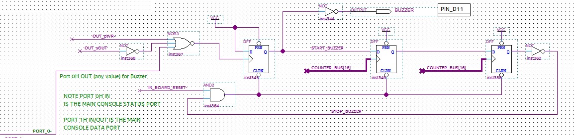
Port 0H is normally an Input port for Console Status. We use it here as an output port to trigger the Buzzer. Note currently, outputting any byte pattern to port 0H will trigger the buzzer.
We will next add a parallel port printer interface for the 26 pin connector P18.
Add U23.
This port is compatible with the IMSAI PIO board. While it does not use 8212's, from a software perspective it behaves the same. This module took way longer than I estimated to get working (3 days). It seems simple enough -- send 8 bits of data to the port, lower the strobe line, when an acknowledge comes back from the printer raise it. Then wait until the printer busy line goes "not busy". All worked fine with a slow Z80 CPU clock of 2mHz, but when I raised the clock speed to 50mHz I would see random duplications of some characters on the printout. I have used two test printers, a HP LaserJet 1012 and a Samsung ML-2525WLaserJet. Same results in both cases.
I tried all the obvious things like adding port IO wait states, software delays etc. In the end (by chance), I noticed that I had to lower the 8 data lines to zero after the acknowledge bit was returned from the printer. If I let them float with their previous value until Busy came back I got errors. This may be unique to the above printers, but with the following circuit printing was always 100% reliable.
To test the printer set DIP SW3 bit 3 to low. The onboard Z80 Monitor is programmed to send all console output characters that goes to the Propeller Console to the printer ALSO when IOBYTE bit 3 is low. Note the port addresses used are, 0C6H & 0C7H -- unlike the port addresses used on our other parallel ports boards.
During the course of this work I noticed that it is very convenient to be able to switch the CPU clock frequency between high and low speeds. I use IOBYTE bit 7 (DIP SW2 LHS switch) to do this. Currently slow speed is 2 MHz, high speed is 25 MHz. You can get to higher speeds by adjusting I/O wait states and removing boards like the bus display board. If strange things happen going forward -- try reducing the CPU clock speed, if need be, use other values for the PLL01_50 clock generator. 25MHz is plenty fast for most applications.
I also allow one in software, to temporally force CPU High speed to Low speed just output to port 07H bit 7 High -- and port 07H bit 7 Low to remove the forced low speed (if the CPU is set to High speed with IOBYTE bit 7). Here is the relevant circuit.
Please note the above is a simple switch. No circuit is present to avoid "runt" clock pulses as for example we have in our 80486 CPU board. Since the is no Z80 opcode cache this is probably OK, but if you use the above in software extensively and you see problems you might consider modifying the circuit . The pulsing rate of LED D10 (Board Active) will indicate high/low CPU speed.
It might be useful at this stage to summarize the uses of the IOBYTE bits and the SW3 switches in a diagram. Remember the IOBYTE value is always reflected by the DIP switch positions SW3. It does not have to be but that's the way the current monitor software is configured.
To test the printer, assemble a 25 pin ribbon cable as shown in the schematic for P18. This layout is inline with the common old PC parallel printer port. Only 8 data lines, the Strobe, Ack and Busy lines are used here. Please note the position of the printer cable pin 1 in the above picture.
The usual drill, to add this module to our growing FPGA program
Within Quartus, close the current Z80_FPGA.bdf file. Note, not the project file (Z80_FPGA.qpf).
Then go outside of Quartus and into windows and delete (or rename) it.
Then take the next more complicated Z80_FPGA13
-- (Add printer, bell, Speed switch).bdf file and copy it to a file
Z80_FPGA.bdf
Then go back to Quartus and open this Z80_FPGA.bdf file and work on it.
Examine, compile and run the Z80_FPGA.bdf file.
Here is a picture of what you should get if you set the IOBYTE switches as shown above. Printers like the HP LaserJet's generally only print a page at a time. So until you send a full page of characters the printer will not print -- it stores them in RAM. You can override this by sending, at any time, an ASCII Form Feed (FF, 0CH) character. In our monitor if you send a '@' menu item this will always send a FF to the printer.
BTW, if you get problems with your printer printout, try lowering the CPU speed or install the low speed "Switch" in your BIOS while printing. Adding I/O wait states is another option. Within the FPGA code you can make them printer port specific!
13. Adding The SD Card Interface.
This is perhaps the most complex aspect of this board. Not only in terms of the software but because today SD cards come in all shapes and sizes. There are numerous articles on the web describing how to determine the type of SD card present and even more articles describing how to "initialize" them. I spent a full week studying the area! The three articles that help me the most are:
Secure Digital (SD) Card Spec and Info
What is the correct command sequence for microSD card initialization in SPI?
and the excellent code example by CC Dharmani, see here
I had grandiose plans initially of writing code to handle all types of SD cards. Reality soon set in! The code below will read and write to today's very common Type 2 SD cards. It would have to be modified to work with the older Type 1 cards. These require a different initialization sequence. Experienced SD programmers may note during the card initialization sequence I add valid CRC bytes to the initialization commands before turning off CRC checking. I also actually set the sector size to 512 bytes . Many programs do not do this but the are reports of some Type 2 SD cards actually requiring these steps.
As to the actual Type 2 cards themselves, they come in two sizes "Regular" and "Micro". The latter are quite common these days (e.g. for mobile phones). This board can use any two of the 3 common SD card adaptors shown here. In other words you can have two SD card drives A & B. (You also can have a third IDE CF card drive).
One of the large SparkFun adaptors is attached to the back of the board. Because we are interfacing the SD card with our 3.3v FPGA we can essentially connect the SD card directly to the FPGA. This is what the SparkFun adaptors do. The Adfruit adaptor runs with a 3.3V supply and is only there because many Arduino users have it.
Using an FPGA really illustrates the utility of these chips. We use our now tried and true SPI interface to talk to the SD cards. Unlike the above case with the RTC SPI interface, the clock/bit stream does not have to be continuous. Data is passed in both directions as 8 bit bytes. This is a good thing too, because the SD commands are 48 bits long! Here is the core SD card SPI interface module.
We will allow for two slave/SD drives. These are selected outside the above module by outputting a bit to the CS* pin of the SD card (SD_CS_PORT).
You will note that we use two SPI clock frequencies. This is because during a cold start, SD cards only communicate over the SPI lines at a slow (~100-200KHz). Once Initilized, this can be jacked up. I use 10MHz here. The 21mux controls this by a high/low bit from the SPEED_PORT.
We will require four I/O ports.
SD_CARD_BASE EQU 06CH
SD_DATA_OUT EQU SD_CARD_BASE ; (6CH) Data to SD CONTROLLER
SD_DATA_IN EQU SD_CARD_BASE ; (6CH) Data from SD CONTROLLER
SPEED_PORT EQU SD_CARD_BASE+1 ; (6DH) HIGH TO READ/WRITE SECTORS WITH HIGH SPEED SPI CLOCK
SD_CS_PORT EQU SD_CARD_BASE+2 ; (6EH) SD Card CS* Select Port
SD_STATUS EQU SD_CARD_BASE+2 ; (6EH) SD CARD Status Port
SD_RW EQU SD_CARD_BASE+3 ; (6FH) Port to pulse SPI Read/Write interface
BTW, the IDE CF Card drive is completely independent of this module. You can have up to 3 drives on this board. Any combination of the above SD Card adaptors is fine also.
Initialization of Type 2 SD Cards.
You can skip this section if you like since what is here is already in the Z80 SD_CARD software describe below.
In order to use an SD card you must first "initialize" it. This requires a series of 48 bit SPI commands. These must be sent in the correct sequence, not continuing forward until the correct response from the previous command is obtained. Sometimes this involves repeated sending of a command.
The commands themselves all have the following structure.
The first byte contains the actual "Command". All SD card commands have the following format 01XXXXXXB.
Here is a list of the commands we use:-
CMD_0: DB 40H,00H,00H,00H,00H,95H,0FFH ; (0+64) CMD0 To Reset the SD Card interface,
CMD_1: DB 41H,00H,00H,00H,00H,0F9H,0FFH ; (1+64) CMD1 Activate Init Process
CMD_8: DB 48H,00H,00H,01H,0AAH,87H,0FFH ; (8+64) CMD8 To check Card Voltage
CMD_9: DB 49H,00H,00H,00H,00H,8FH,0FFH ; (9+64) CMF9 Read SD Register (CSD)
CMD_13: DB 4DH,00H,00H,00H,00H,081H,0FFH ; (13+64) CMD13 Get SD card status
CMD_16: DB 50H,00H,00H,02H,00H,081H,0FFH ; (16+64) CMD16 Set Sector size to 512 Bytes
CMD_17: DB 51H,00H,00H,00H,00H,0FFH,0FFH ; (17+64) CMD17 Read a single block (Block 0, Used to load boot sector only)
CMD_41: DB 69H,40H,00H,00H,00H,077H,0FFH ; (41+64) CMD41 Activates the card's init. process.
CMD_55: DB 77H,00H,00H,00H,00H,065H,0FFH ; (55+64) CMD55 Application specific command NEXT
CMD_58: DB 7AH,00H,00H,00H,00H,0FDH,0FFH ; (58+64) CMD58 Read SD Cards OCR register
CMD_59: DB 7BH,00H,00H,00H,00H,0FDH,0FFH ; (59+64) CMD59 Turn off CRC checking
You will note there is always a "stuffer" byte 0FFH byte sent before a return response byte(s) from the SD Card. The return Flag byte contains the error code if any. Generally (but not always), you want to receive 00H.
The sequence to initialize Type 2 SD cards is as follows.
Drive the CS* pin from high to low
Send 12 or more dummy 0FFH bytes
Then send the following 6-byte command, First byte: 0x40 (CMD0), Next four bytes: 00000000H, then the CRC byte (95H), then send another dummy byte 0FFH byte.
Read the returned byte from the SD Card. If its not 01H, repeat this command until 01H is returned.
This means the card is in the "idle state" and we are good to go.
Next send the following 6-byte command, First byte: 0x48 (CMD8), Next four bytes: 000001AAH, then the CRC byte (87H), then send another dummy byte 0FFH byte.
Read the returned byte from the SD Card. If it is 01H you probably have a Type 1 SD card. We want a 05H returned, indicating a Type 2 card.
We confirm this by reading the next 4 bytes from the SD card. If its 000001AAH, we have a Type 2 card for sure.
Next we "activate" the Type 2 card by sending two back to back commands CMD55 and CMD41 exactly as done above for the CMD0 command.
Repeat the latter two commands continuously until you get a return 0H byte.
The SD card specifications says that only CMD0 and CMD8 should have a valid CRC byte in SPI mode, however there are reports that some SD cards (like Transcend ones) seem to require a proper CRC for CMD55/CMD41 commands as well. To be on the safe side I add the byte.
Also between every command above, the SD card CS* line needs to be lowered and raised when done.
Based on other web postings, I also send CMD59 to specifically turn off CRC checking and CMD16 to set the sector size to 512 bytes/sector.
I'm not convinced these are essential but it's best to play safe.
Here is an example picture of the main SPI signals using the CMD8 command:
I have written a small Z80 program to initialize, read and write sectors to the A and B SD drives. It is called SD_CARD.Z80. And can be downloaded at the bottom of this page. Again, this is a standard S100 bus program that can be downloaded from your PC via the FPGA monitors "X" command. It starts in RAM at 100H. So we use X100. The program allows you to test the SD Cards interface.
Here is a picture of the main menu:-
Please note this is not a "bullet proof" program. Little command error checking etc. is done. The sector numbering is only 0-FFFFH, but that should be enough for most needs. In fact some older Type 2 cards may not accept a sector number this large. You may have to hit the CMD0 command twice to initialize a newly inserted card or on power up.
Note. These SD cards can read and write multiple sectors with one command. I have not added this feature yet.
Of course before you run the above program you need to add the above SD Card interface module to our growing FPGA program.
Within Quartus, close the current Z80_FPGA.bdf file. Note, not the project file (Z80_FPGA.qpf).
Then go outside of Quartus and into windows and delete (or rename) it.
Then take the next more complicated Z80_FPGA14
-- (SD cards Done).bdf file and copy it to a file
Z80_FPGA.bdf
Then go back to Quartus and open this Z80_FPGA.bdf file and work on it.
Examine, compile and run the Z80_FPGA.bdf file.
Do spend some time studying the FPGA ports and the above Z80 code.
All the critical routines: Initialize, Read Sector, Write Sector etc. are written as self-contained returnable calls which should make it easier to incorporate them as a CPM BIOS etc. The source is in Zilog and Intel formats. The latter for CPM's RMAC.
Here is a picture of the final setup:-
The card LED's are a little confusing, with the SD/MMC card adaptor, the relevant LED (D21 or D20) will light up if a SD card is inserted.
The micro SD card adaptor lights up if the card is not inserted.
Note you cannot use two different cards on the same drive (A or B).
Note also, some cards require the Initialization routine to run twice (i.e. the 0
menu option) to initialize without an error.
One final note, a useful PC program to see/check what is written on any sector of an SD Card is HxD Hex Editor.
It can be downloaded from here.
14. Adding Interrupt Processing.
Interrupts are not commonly used on single user Z80 S100 bus systems. That said the Z80, for its time, had some powerful interrupt capabilities.
The Z80 actually has four different interrupt modes instead of the 8080's two (INT & NMI). It has the NMI or non-maskable interrupt mode exactly like the 8080 where if pin 17 is pulled low, the Z80 will always immediately jump to location 66H in RAM. This mode is only used for power fail warning circuits etc. and is not of much general use. All other interrupt modes use the "real" Z80, pin 16.
INT Mode 0. This is identical to the 8080 Interrupt. If the Z80 is programmed to operate in this mode, it will expect a device to place on the bus after a single INTA signal -- one of the 8080's "RST vectors". These are:-
| | | RST# | OP Code | Bit Pattern | RAM Location | | RTS 0 | C7 | 11000111 | 0000H | | RST 1 | CF | 11001111 | 0008H | | RST 2 | D7 | 11010111 | 0010H | | RST 3 | DF | 11011111 | 0018H | | RST 4 | E7 | 11100111 | 0020H | | RST 5 | EF | 11101111 | 0028H | | RST 6 | F7 | 11110111 | 0030H | | RST 7 | FF | 11111111 | 0038H |
|
Note, if no device places an RST 8 bit vector on the bus after the INTA signal, the bus will float (typically to 0FFH) and cause the Z80 to always jump to location 38H in RAM.
INT Mode 1. This is a special Z80 interrupt which if the Z80 is so programmed to operate in this mode it will always jump to location 38H in RAM. This mode is very useful for testing software. Just temporally grounding pin 16 of the Z80 should force the CPU to jump to 38H in RAM.
INT Mode 2. This is a special Z80 interrupt which if the Z80 is so programmed to operate in this mode has an extremely powerful interrupt feature. Again the Z80 sends out an INTA signal and expects to see an 8 bit vector on the data bus. However this time the 8 bit vector is combined with the special Z80 interrupt register "I" to generate a 16 bit interrupt vector address. In this mode the Z80 can be forced to jump anywhere in its 64K address space to an "interrupt vector routine address". Note it is a 2 byte address of the routine - not the routine itself. In other words a two byte pointer. Low byte first, high byte second.
The S100 bus allows for 8 separate interrupt "identification" lines which tells an S100 bus interrupt controller which interrupt has priority and should be (first) processed by the CPU. For 16 bit, (and greater), PC systems, almost universally the interrupt controller is an Intel 8259A type controller. Unfortunately that controller is not easy to interfaced with a Z80 and so an equivalent "8259A" FPGA module would not be useful. In the end I settled on an FPGA module that is a modification of the PDP11 Interrupt Controller we used on our PDP11 Support board. Lets look at the circuit.
We will use here the powerful Z80 Mode 2 for all interrupts. I will address the simpler Mode 0 (8080) and Mode 1 later.
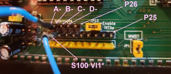
First we will track/pritorize up to four separate incoming interrupts from the eight S100 bus interrupts. We do this by wire-wrapping/jumpering P25 & P26 (see picture below).
Here is the core FPGA Interrupts Circuit:-
Interrupt signals arrive at the 74148 (via the 74373). Two things happen. The highest priority signal sends out as a 3 bit pattern to the 74244. Also a low signal comes from the GS* pin of the 74148. This triggers the INT pin of the Z80. When the Z80 is ready, it lowers the OUT_sINTA input to the 74373. This latches the Interrupts inputs which allows the 3 bit pattern to merge with the ground bits of the 74244 to place an Interrupt vector on the Z80's Data bus. This is the lower 8 bit "interrupt vector" address which when combined with the 8 bits in the Z80's "I" register provides a 16 bit Interrupt vector address. The Z80 jumps to the routine that address points to. Within that "interrupt routine" we print a message on the screen. It then re-actives the Z80 ability to receive another interrupt (EI) and does an interrupt return (RETI).
The location of the interrupt pointers and the actual interrupt routines must be carefully placed. The vectors can in fact be anywhere in the Z80's 64K address space. However usually they are placed in the CPU first page (0-FFH). In other words we place 0H in the Z80's I register. Now the low byte, traditionally people like to use locations that the 8080 used. It does not have to be, but it simplifies software. In the layout above the following 4 locations are used:-
| | | FPGA Pin | 74148 Output (A,B,C) | Bit Pattern | RAM Location | | FPGA_IN_INT_A- | A+B+C | 00111000 | 0038H | | FPGA_IN_INT_B- | B+C | 00110000 | 0030H | | FPGA_INT_IN_C- | A+C | 00101000 | 0028H | | FPGA_IN_INT_D- | C | 00100000 | 0020H | | RTC_INT | (not currently used) |
| |
|
Clearly within the FPGA code you can move the interrupt vectors around any way you like. You can change the input bits to the 74244 or 74148. You can also change the RAM page. If you used:-
LD A,20H
LD I,A
IM2
EI
You would place the interrupt vectors between 2000H and 20FFH.
Two things to remember. The above locations are only 16 bit pointers to the an actual interrupt routines. Second every interrupt routine must end with:-
EI
RETI
You need to re-activate interrupts when done. The special RETI opcode is actually only for Zilog support chips - it behaves the same as RET.
Lets load the above module to our growing FPGA program. Add Jumper JP10.
Within Quartus, close the current Z80_FPGA.bdf file. Note, not the project file (Z80_FPGA.qpf).
Then go outside of Quartus and into windows and delete (or rename) it.
Then take the next more complicated Z80_FPGA15
-- (interrupts Added).bdf file and copy it to a file
Z80_FPGA.bdf
Then go back to Quartus and open this Z80_FPGA.bdf file and work on it.
Examine, compile and run the Z80_FPGA.bdf file.
We will use the keyboard interrupt generated by our Propeller Console IO board. If you don't have it set on this board -- read up on it and do it now. Normally we use Interrupt vector S100 bus pin 5 (IV1*). Whenever ANY keyboard character is pressed Int IV1* will pulse low. We use the Z80 FPGA SBC board jumpers on P25 & P26 to assign interrupts to the FPGA module. Here is a picture:-
| |  |
To test the interrupt module I wrote a short Z80 program called Z80_INTS.Z80. It can be downloaded from the bottom of this screen to your PC.
You the use the Z80_FPGA Monitor "X" command to load it to 100H in your S100 bus system.
The following picture should say it all:-
You can switch around the four P25 interrupts inputs to test the various interrupt routines.
If you wish to bypass this circuit just remove jumper JP10. You can then have another S100 board trigger an interrupt (via S100_INT-). That board must of course look after its own interrupts pritorizing upon receiving the Z80 sINTA signal and place the appropriate interrupt vector on the S100 bus Data In lines. Our old Interrupt/RTC board for example could do this.
INT Mode 1.
This Z80 interrupt mode by comparison is very simple. If this mode is active and the Z80 INT pin is pulsed low the Z80 will always load the interrupt vector at 38H in RAM -- no exceptions. The pointer at 38H & 39H point to the interrupt routine. Remember low byte in 38H, high byte in 39H. No other "hardware" is required. This mode is very useful for writing and testing interrupt routines. In the above Z80_INTS.Z80 example, when Mode 1 is active, pressing any keyboard character will force a quick beep from the boards buzzer.
BTW the NMI interrupt routine (not currently used here) is exactly the same except the location is 66H in RAM
INT Mode 0.
This mode is the exact same as the only mode the 8080 CPU has. Its actually quite different. When the Z80 is in this mode any time its INT pin is pulsed low it sends out a interrupt acknowledge signal (actually for the Z80 a special M1+IORQ signal). The hardware seeing this signal puts a special 8 bit data byte on the Data In bus. One byte that's it. Both the 8080 and Z80 have eight special single byte opcodes which if detected force the CPU to jump to one of 8 RAM locations in the first page of RAM (0-FFH). They are called RES opcodes.
Here they are again:-
|
| | | | RST# | OP Code | Bit Pattern | RAM Location | | RTS 0 | C7 | 11000111 | 0000H | | RST 1 | CF | 11001111 | 0008H | | RST 2 | D7 | 11010111 | 0010H | | RST 3 | DF | 11011111 | 0018H | | RST 4 | E7 | 11100111 | 0020H | | RST 5 | EF | 11101111 | 0028H | | RST 6 | F7 | 11110111 | 0030H | | RST 7 | FF | 11111111 | 0038H |
|
|
So if the interrupt hardware for example slams 0EFH on the data bus, the Z80 will always jump to location 28H in RAM and start from there -- no exceptions - always.
To implement the INT Mode 0 in our FPGA module we would simply have to change the bit pattern put out by the above 74244. A pattern of 1110111 would cause the Z80 to jump to location 28H in RAM. Note in this case 28H is not a pointer, actual interrupt code must reside there, Its of course usually a JP instruction.
This concludes our interrupt section. To be sure you understand the process (and the previous RTC section) try utilizing a one second RTC interrupt to generate a buzzer beep.
For those that do not have the Propeller Console IO board, you can generate a crude interrupt by briefly grounding the S100 bus VI1* pin. You will also need to change the console I/O routine in Z80_INTS.Z80 to the USB port output. See the FPGA_Z80 monitor for details.
15. Adding an SPI interface and Real Time Clock/Calendar.
We will now add the Clock/Calendar Maxim DS1305 chip U2 to the board. Add the small 32.768 KHz crystal (X1). (Also add the CR2032 3V "coin" battery). This is a simple, but an extremely powerful, 16 pin DIP chip. It will handle almost any date/time requirement you have. It is described in detail here. As you can see the interface can be via a SPI or I2C connection. I have chosen an SPI interface (Pin 9 of the DS1305 to Vcc33).
I had some difficulty getting this chip to work initially. I was not sure if the problem was with my FPGA software or the board hardware. To eliminate the former, I first
temporally installed a known good SPI module and patched it up to a 128K SPI Serial 128k AT25128 Atmel EEPROM described previously here.
Here is a picture:-
You simply patch the wires to the appropriate EEPROM socket pins. In
recommend doing things like this when bringing up new SPI/I2C interface chips. After I satisfied myself that the core SPI FPGA code was correct. (The actual FPGA code is
in Z80_FPGA_EEPROM.bdf, but you should not need it here). I then switched in the RTC chip. I wrote a short Z80 program to interface with the FPGA RTC chip. (It can be downloaded from the bottom of this page and is called SPI_RTC.Z80) .
Add the RTC chip U2 (a DS1305) and the 32.768KHz crystal. Also add the CR2032 coin 3V battery.
I spent two days before I got it to respond! Long story short...
Unlike our previous SPI chips this RTC chip will not tolerate a brake in the clock signal as bytes are sent to it. With the above EEPROM for example, you can send 8 bit data bytes one at a time and so long as you keep CS active they will all be collected by the SPI chip. With this RTC chip no clock delays are tolerated between bytes. For SPI writes we need to send two byte commands (a register address and its data). These must be assembled into a 16 bit value and sent as one SPI signal. Fortunately the read/returned SPI data is always 8 bits. I had to modify our SPI module accordingly. I named it SPI_16bit_MASTER.bsf. Here is the core SPI module to interface with the RTC.
The Z80_FPGA.bdf had buffers to accommodate the 16 bit interface.
The usual drill, to add this module to our growing FPGA program
Within Quartus, close the current Z80_FPGA.bdf file. Note, not the project file (Z80_FPGA.qpf).
Then go outside of Quartus and into windows and delete (or rename) it.
Then take the next more complicated Z80_FPGA16
-- (Added RTC Chip).bdf file and copy it to a file
Z80_FPGA.bdf
Then go back to Quartus and open this Z80_FPGA.bdf file and work on it.
Examine, compile and run the Z80_FPGA.bdf file.
In order to test the chip/interface
from the main menu enter the "L"
command.
Here is a picture of the main menu:-
A useful feature of this chip is a 96 byte NV RAM storage area, (Provided you have battery backup).
Upon power on (no battery backup) the chip must be "activated". With battery backup you only need to do this one time. If you do it again/later it will reset the time to 0's.
For those that want to see what the SPI signals look like. Here is a picture with the Menu command "1", to read he seconds register.
One final note; in an earlier prototype board I had Vcc (pin 16) of the RTC chip set to the 3.3V supply. I found the CR2032 3V "coin" battery voltage was not sufficient to overcome triggering the "Power Fail" signal (pin 15) when the RTC was in battery mode and a chip Vcc of 3.3V. This inactivates reading the chip signals. Fortunately the chip Vcc can be connected to the 5V supply and via (pin 14 connected to the 3.3V supply), still interface directly to the FPGA pins. BTW its useful to protect the back +3V battery pin on the back of the board with a patch of black insulating tape to prevent a short-circuit when laying the board down on the bench.
Burning FPGA Code to Flash RAM
Up until now whenever we programmed our FPGA via the JTAG socket the data is lost whenever the power is turned off. While fine for code development etc. it is not desirable for a final board configuration. Like most FPGA applications the "final" code is saved in Flash RAM and immediately loaded by the FPGA each time upon power-up. This is a standard and common characteristic of most FPGA's. Some older models in fact had a ROM onboard. Our Cyclone IV Adaptor board has 16MB of Flash RAM on board for this purpose -- way more than we are ever going to need!
The tricky part is programming this Flash RAM. I found the Intel documentation poor and confusing. Here is a summary of the process:
Within Quartus you need to "convert" your normal JTAG FPGA .sof programming file to a special file .jic to program the Serial Flash RAM chip on the Weveshare board.
Within Quartus, click on the File Menu and select "Convert Programming files". The dialog box below will popup.
From the dropdown box on the "Programming File Type" select a .jic file type.
This is the file format that is required to program the onboard serial Flash RAM.
For the Options/Boot info select EPCS16. Leave Active Serial as is.
You can name the .jic output file anything you like. I usually just leave it
output_file.jic.
Note it will be in
the Quartus work directory.
Next click on Flash loader within the lower "Input Files to Convert", then click on the highlighted "Add Device" button.
You will get a popup dialog box as shown below.
Select Cyclone IV and EP4CE10. Note Quartus takes some time to allow you to actually select these options -- seems to be doing things in the background!
Next click on "SOF Data" and "Add File". You should see your "normal" FPGA program .sof file in your "output_files" folder within your work directory.
Finally click the "Generate" button.
You should get a popup dialog saying "Generated
output_file.jic successfully.
Note the name and location of the converted file. Then close that dialog box. See the pictures below.
Two things, first for some reason Quartus often takes a long time (~30 seconds) to locate/display the directory (usually output files) you want to deposit the .jic file
Second, in the next step its essential you point to the correct jic file you just made. If in doubt, label it xxxx.jic above.
Next we need to actually flash the Waveshare boards RAM chip.
Click on the normal "Program Device (Open Programmer)" you normally use. If its not already open, give it time to come up as a dialog box.
Make sure your board has power. To be safe click the Auto Detect button. your normal xxx.sof file should display with the device set as EP4CE10F17.
First delete the above line xxx.sof | EP4CE10F17 etc.
Click on Add File and select the output_file.jic file you just generated above.
Click on the Program/Configure little square character boxes.
The chip diagram below should show only 2 chips as shown. If more right click on any 'extra' one and delete it. The dialog box must look as shown below.
The Start button should highlight.
Click on this and you will flash the RAM chip. Follow the Progress bar until it is done -- it takes about 1 minute.
You can power off and re-power your computer.
Your FPGA board should (after reset), start with whatever FPGA code is within the chip.
Note when you close the above dialog box, normally you do NOT save the changes.
Typically you want the chip to be quickly reprogrammable with .sof files.
Notes
A small error has been noted by Steve Osborne, two
pull-up resistors for the SD Card adaptor are incorrect. As pointed out by Randy McLaughlin it can be
easily corrected as shown here.
Richard Camarda has noted that while outputting 02 to port 07H does indeed inactivate the FPGA ROM it does not release the underlying RAM from F000H to FFFFH.
He has provide the following FPGA code correction. Thanks Rick.No other hardware/software changes have been noted to date.
A Self Contained Board
This Board is a completely self contained S100 Bus Master as defined by the IEEE-696 Specs. It can therefore be run outside the S100 bus if you simply provide power to it. There are two pins P31 for ground and P30 for 8-10V input to do this. Please use the upmost care in doing this. Make sure the board is sitting on an insulated background (glass/wood etc.). Of course you will want to configure the IOBYTE to the USB port or VGA and PS2 keyboard.
Parts
There appears to be a few variations of the 74LVC245 20 pin DIP level Shifters chips with "A", "AN"
etc. after the 245. As best I can tell so long as they are 20 pin DIPs they are all OK. I use Mouser chips # 595-SN74LVC245AN.
The WaveShare Cyclone IV adaptor can be obtained directly from Waveshare.
You also might want to get the USB Blaster/Programmer from them.
The WaveShare unit uses unusual 2mm dual row pin connectors. Unlike to normal 0.1" connectors these are quite rare an expensive (Digi-Key #S5750-30-ND). You need to carefully cut them to size, carefully cutting off the extra pins with a wire cutter. The USB serial Adaptor is from Sparkfun F1231x. The Micro SD Card adaptor is from AdaFruit.
Please note the Digi-Key #S5750-30-ND sockets for the WaveShare adaptor are quite tricky to fit on to the board. I found the best way to do it is (after trimming to size), push them half way on to the adaptor pins and then wiggle them to fit the whole unit on to the S100 board. Figure on spending 10 minutes on this step! Do not solder them to the board first and then try and press the adaptor down on them. They are very fragile and internally the leaves will bend if socket angles are not exactly correct. When in place, check each pin is visible on the back of the board before soldering. Only then solder all around. Add as little solder to each pin as possible - the narrow pins have a tendency to wick up solder internally.
Leonard Young recently pointed out better sockets are available from Mouser (Preci-dip 833-87-038-10-001101) as part 437-8338703810001101 for $3.04 ea. You’ll need a few, since 38 positions is a 2x19 strip. Mouser seems to stock low numbers however. DigiKey is somewhat better. They have a 100 pin equivalent socket (#1212-1786-ND) for ~$6.50.
To remove the adaptor, leaver each corner up a little going round and round. The first time its quite difficult to get the adaptor out. It gets easier with time.
Finally please note the actual final board sent to users is labeled "V1.1b". There were some very minor changes made in this version over the one displayed here. Here is a picture of the V1.1b everybody
received.
If you wish to utilize the IDE card, SD/MMC card and MicroSD card all together you may wish to modify the IDE two row pin connector so the adaptor is higher up over the SD card adaptors. There may be wire-wrap two row pins -- I have not checked. I used the following "kludge":-
Be sure all pins are connected and not shorted to a
neighbor pin.
Note experienced board builders can program the
FPGA board with the Z80_FPGA_Work_Folder.zip
and run Z80FPGA.bdf
directly skipping all the
intermediate steps above.
CPM Images
There are numerous CPM3 CF card images you can download to run on this card.
It's best to start with a simple "Non-banked" system such as the
CPM3 CF Card Image #1.
Write that image to a CF card using the
HDD Raw Copy Tool
described on that page. It should boot immediatly with the monitor "P"
command.
Not-banked CPM3 will require you to extensively modify your CPM3 BIOS to switch
in/out RAM pages. I have not done this yet!
Notes
Wayne Warthen has kindly supplies some
updates to the Z80 monitor. It can be
downloaded from here.
Bugs
So far no hardware bugs have been noted with the board.
However it has been noted that the early versions of Z80 CPU FPGA code does not
implement the Z80 block IO instructions (OUTI, INI) correctly.
The OUTI instruction was used to initialize the Z8530 dual serial chip on our
Serial board. The
board speech synthesizer and XModem command did not work.
This has now been corrected. The version below implements all Z80 instructions
correctly.
A Production S-100 Board
Realizing that a number of people might want to utilize a board like this together with a group of people on the Google Groups S100Computers Forum, a "group purchases" was formed. It is now closed.
Please see here for more information. Please do not contact me directly.
FPGA Z80 (V1.1) - FPGA Z80.zip This .zip file contains all the KiCAD components to build the S100 board (V1.1 9/6/2019)
FPGA_Z80 (V1.1) Schematic.pdf This .pdf file contains the complete board schematic (V1.1 9/6/2019)
FPGA Z80 SBC (V1.1b) Gerber.zip Gerber files to manufacture the board. (V1.1 b 9/10/2019)
SBC-Z80-FPGA Work_Folder.zip
(This .zip file contains the Quartus file folder to run all the examples on this
page. 8/7/2023)
SBC-4K-MONITOR.HEX (This .HEX file contains the file for the
8K Quartus ROM) (8/7/2023)
SBC-MON_ABCD.HEX (This .HEX file contains the file for the
16K Quartus ROM) (8/7/2023)
output_file.jic
(Final compiled file to burn into the FPGA)
Quartus-lite-18.0.0.614-windows.tar This is a .tar file containg Quartus Lite and support programs. Note it's almost 6GB in size (11/10/2019)
Z80_FPGA CPU Board S100 Bus Programs.zip This .zip file contains a number of small Z80/S100 bus programs to test the board (V1.1 9/6/2019)
Z80_FPGA Board Layout Supplied by Rick Bromagem (V1.0 11/11/2019))
Z80_FPGA Board BOM (.xls) Supplied by Rick Bromagem (V1.0 11/11/2019))
Z80_FPGA Board BOM (.pdf) Supplied by Rick Bromagem (V1.0 11/11/2019))
Complete KiCAD folder in a .zip file to construct the board (Final 4/2/2020)
S100Microcomputer_Folder (For Jeff & Terry)
Other pages describing my S-100 hardware and software.
Please click here to continue...This page was last modified on
02/29/2024

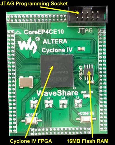
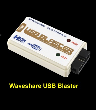
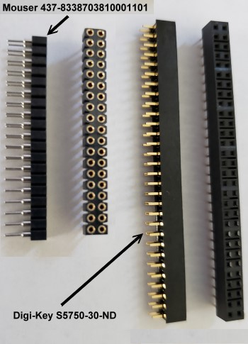
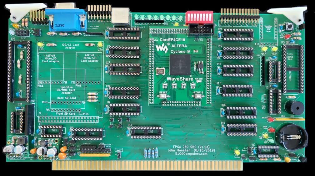
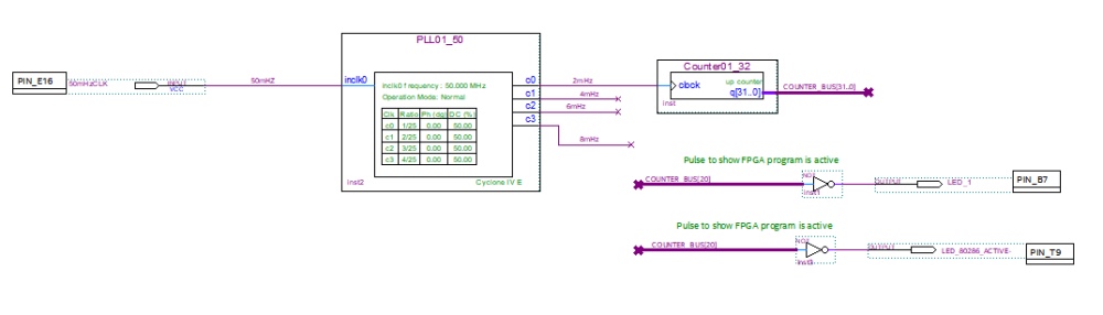
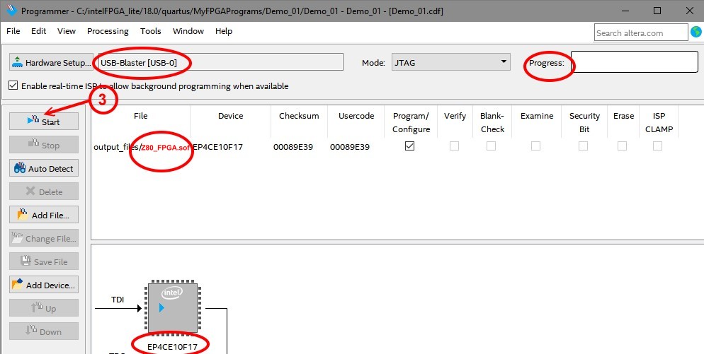
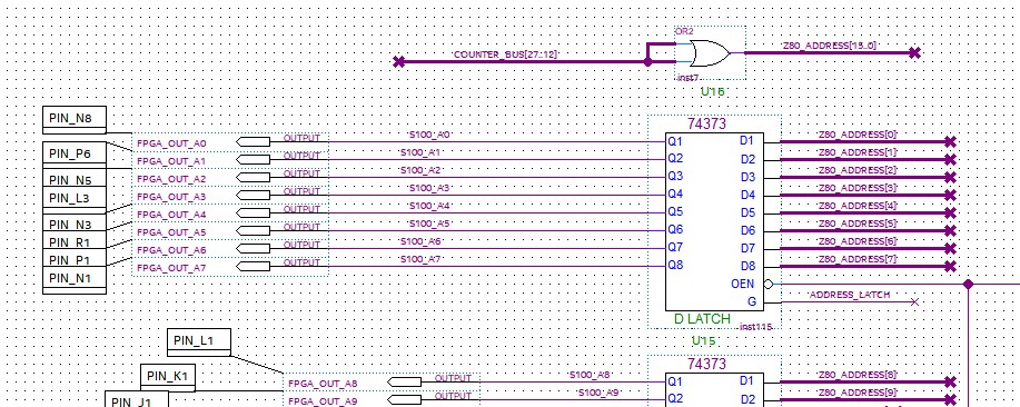


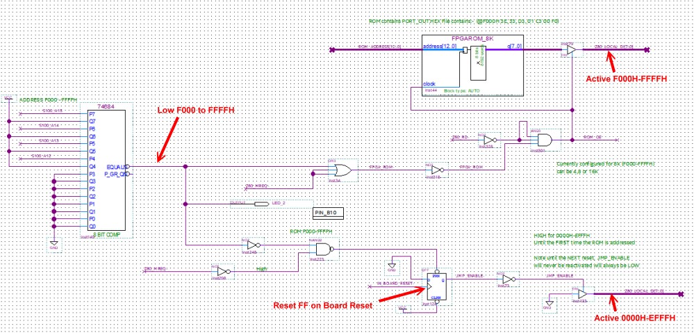
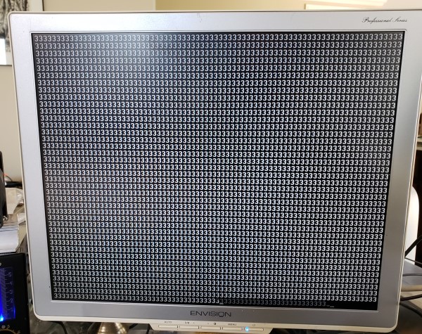
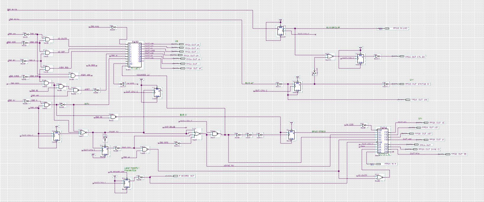
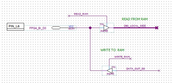
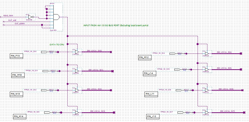
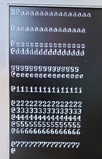

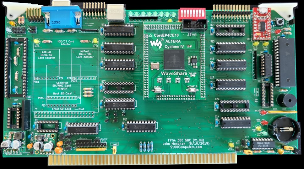

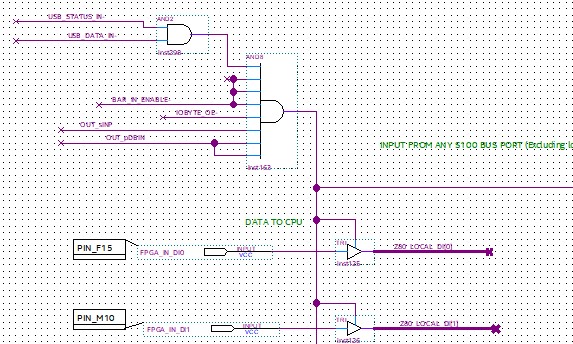
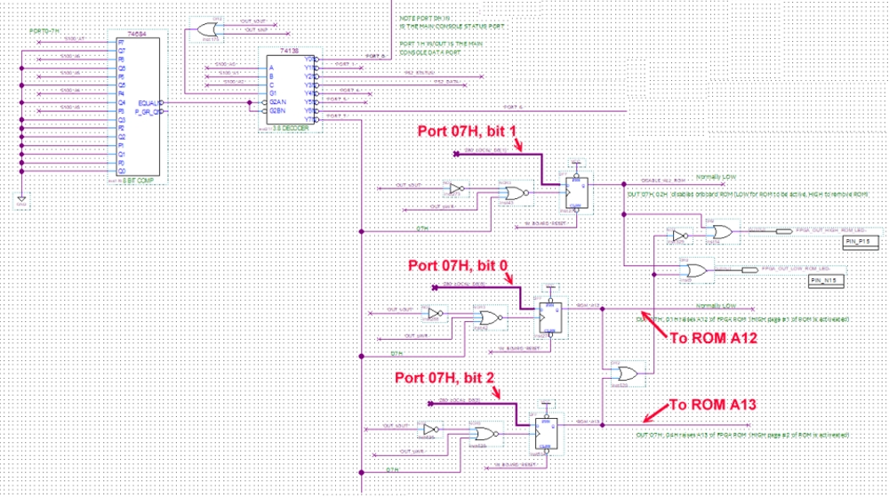
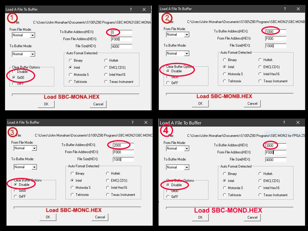

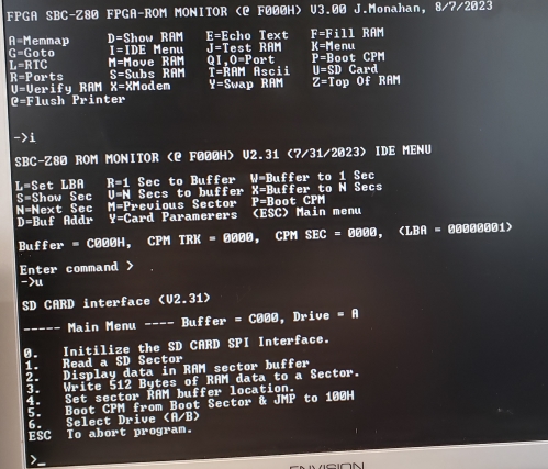
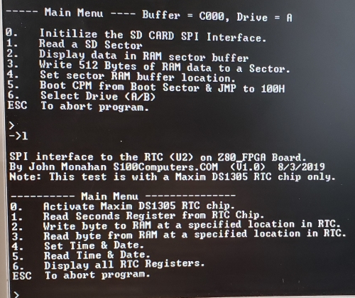
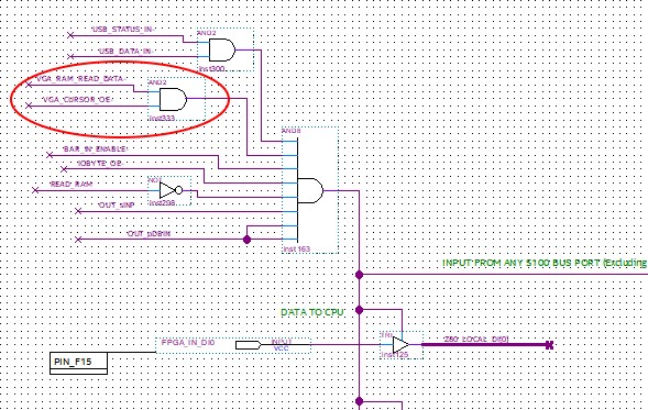
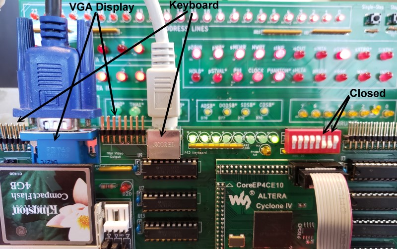
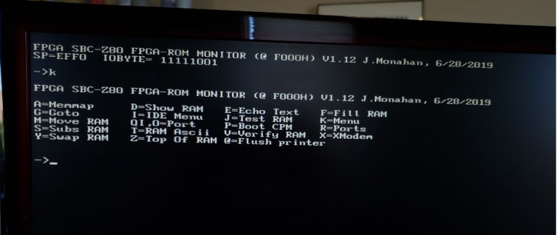
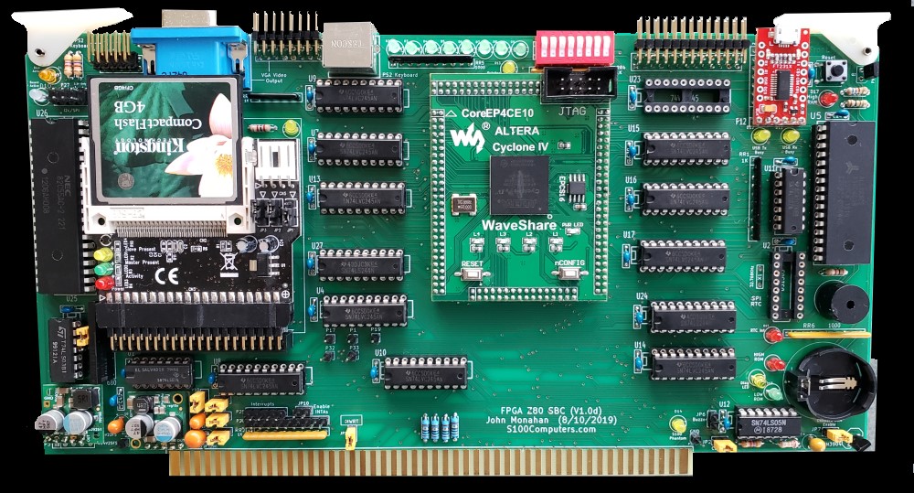
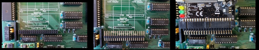
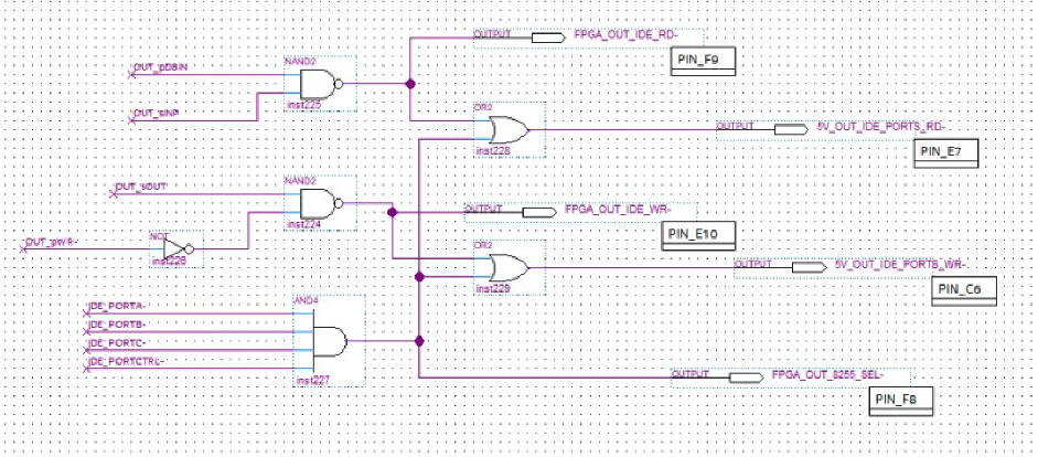
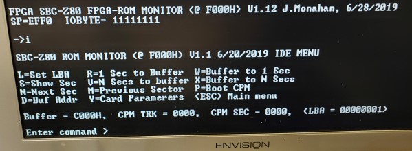
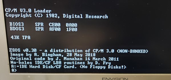
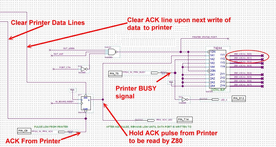

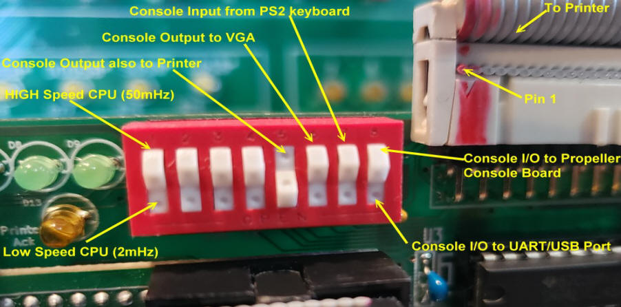
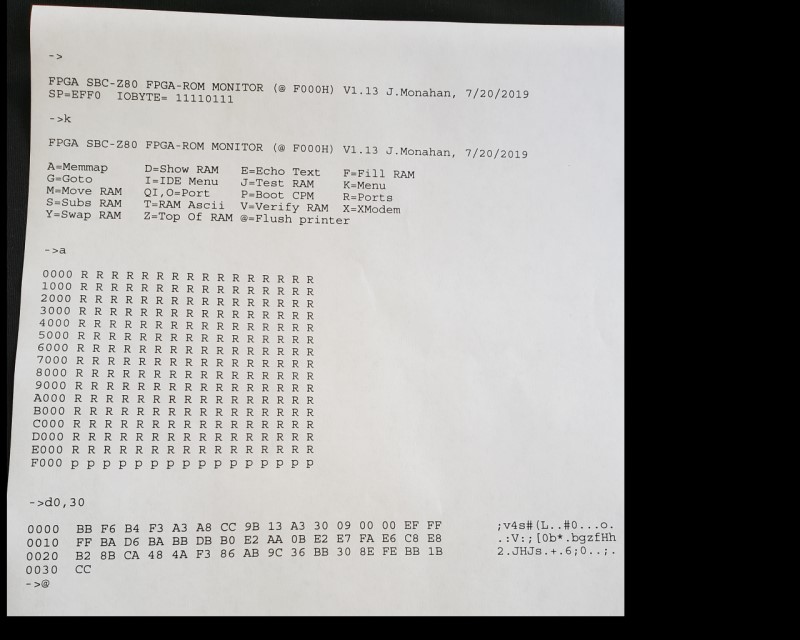
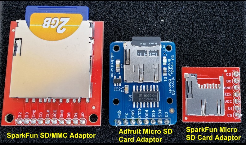
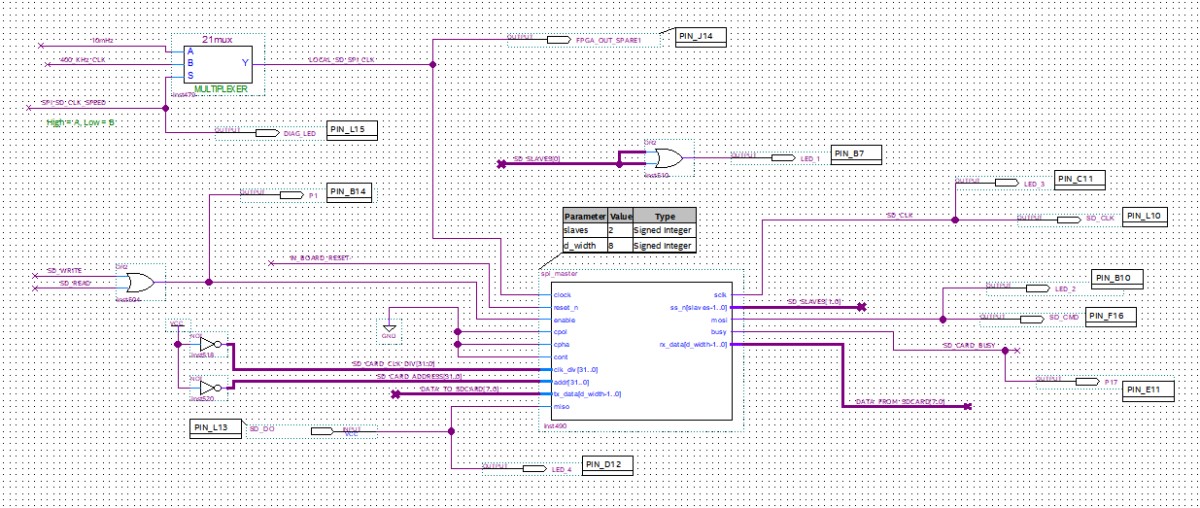
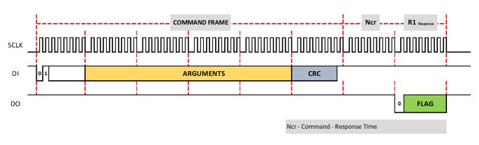
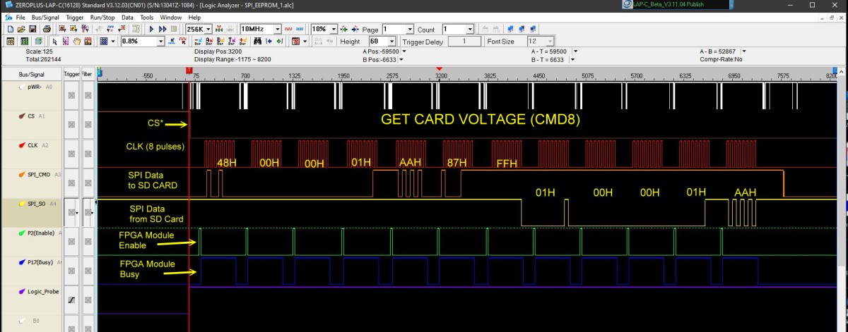
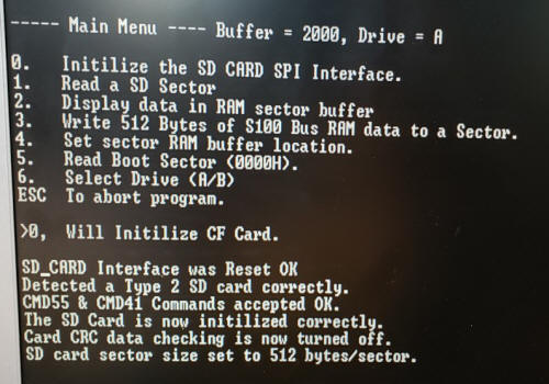
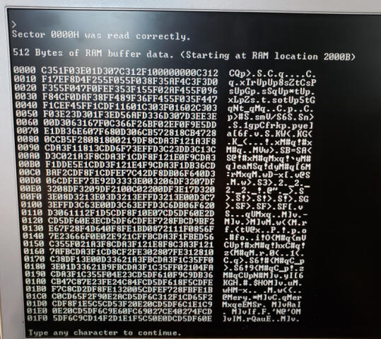
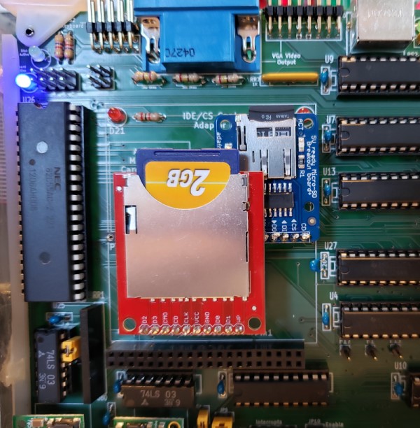
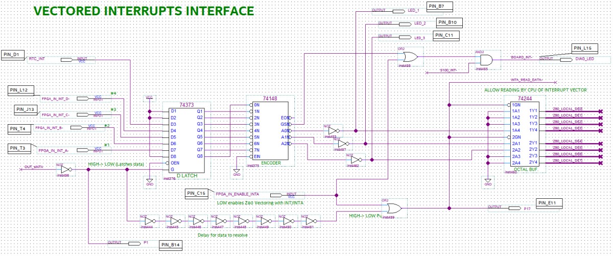
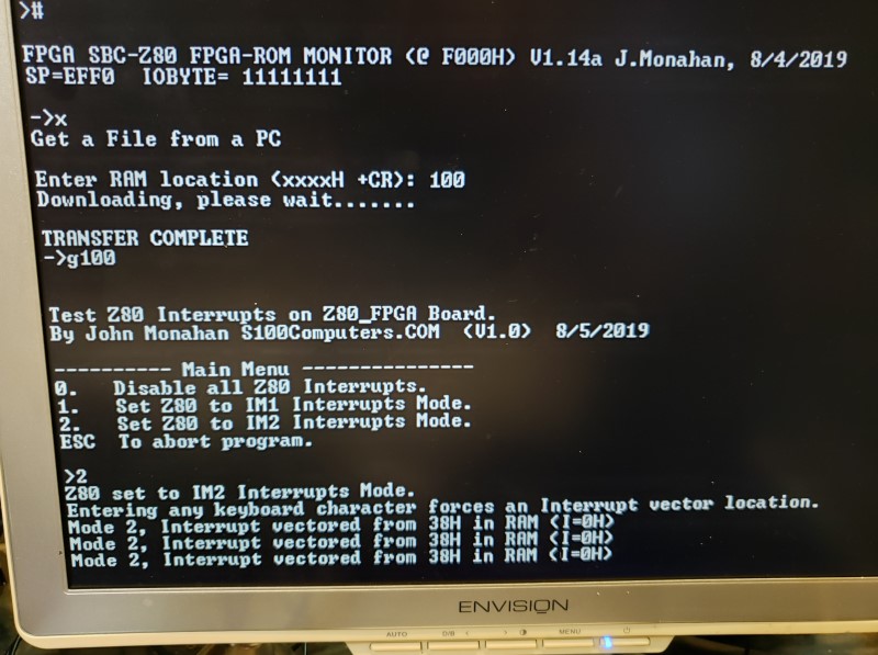
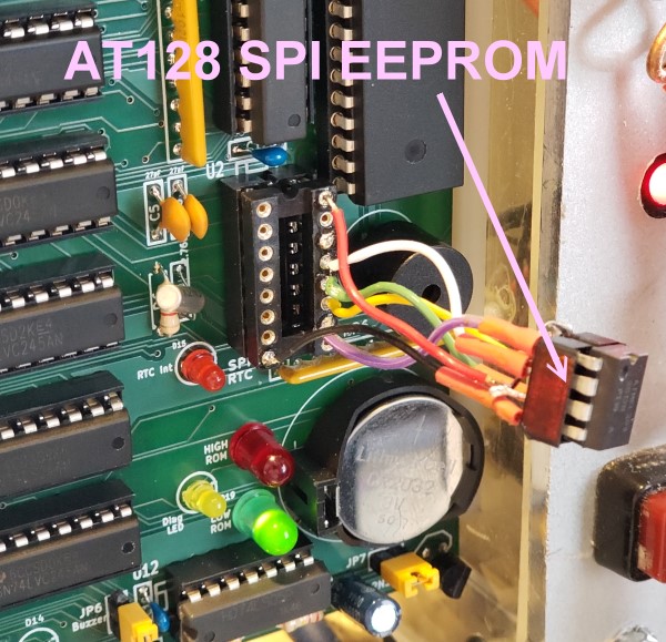

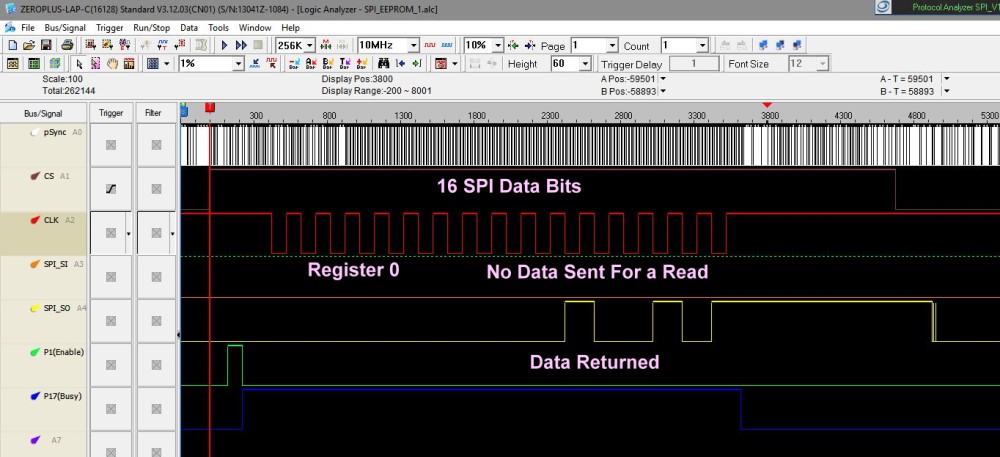
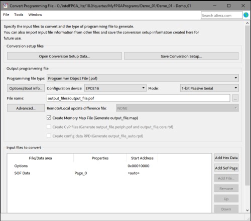
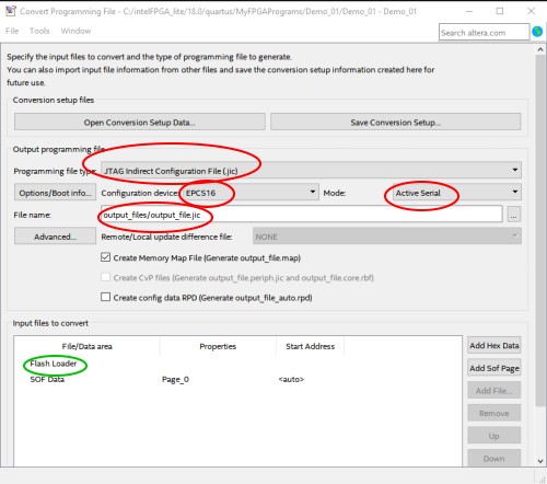
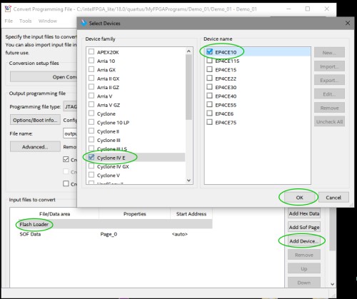
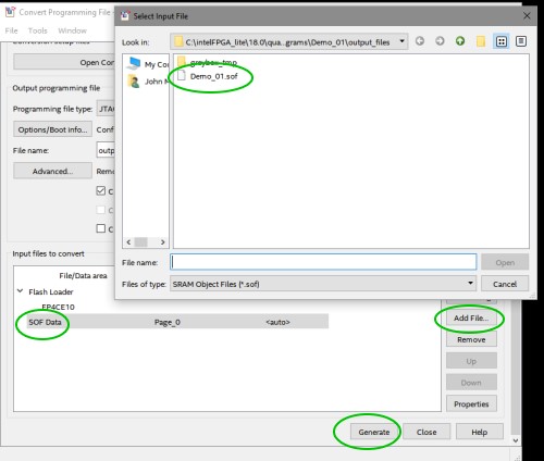
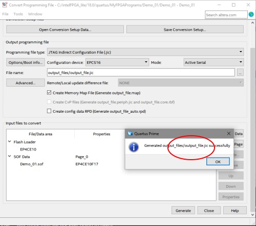
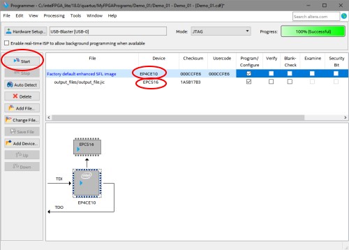
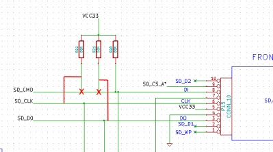
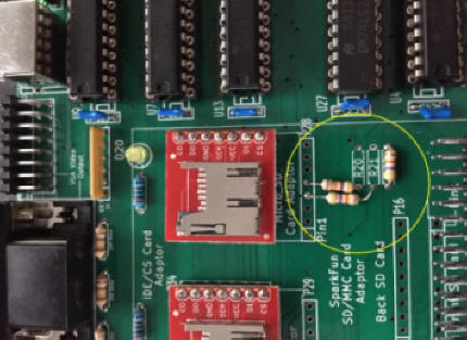
.jpg)