S100 banner
Home S-100 Boards History New Boards Software Boards For Sale
Forum Other Web Sites News Index    

FPGA and Quartus Programming
Introduction
A field-programmable gate array (FPGA) is a natural extension of CPLD's and those a natural extension of the GALs we used on earlier boards.  It is in effect an integrated circuit designed to be configured by a customer or designer after manufacturing – thus the name "field-programmable". The FPGA configuration is done using a "hardware description language" (HDL).  There are two major languages Verilog and VHDL.

Verilog was created by Prabhu Goel, Phil Moorby, Chi-Lai Huang and Douglas Warmke around 1984. Originally, Verilog was only intended to describe and allow chip hardware simulation. The automated synthesis of subsets of the language to physically realizable gates etc. was developed after the language had achieved widespread usage. Verilog stands for the words "verification" and "logic". There were many upgrades/extensions over the years. The last major version appeared in 2005.

VHDL was originally developed for the U.S Department of Defense in order to document the behavior of the ASIC chips that supplier companies were including in equipment. Because of this background much of the syntax was based on the Ada programming language. The language has undergone numerous revisions and has a variety of sub-standards associated with it that augment or extend it in many ways, the last major release being in 2008.

Usage between the two tends to be polarized. Probably because of its Ada/Pascal style VHDL seems to be more popular in Europe.  The "C'" style syntax Verilog seems to be more popular in the US. 

Overlaid upon this are the chip "hardware camps".  Just like the original CPU chips, there are a number of FPGA chip manufacturers.  However there are two dominant players Xilinx and Altera.   Recently Altera was acquired by Intel so I will refer to is as Altera/Intel.  Much of the information on the web still appears under the name Altera.   Both groups by now seem to have endless variations of their FPGA chip families.   The major ones are:-

Xilinx -- Spartan
Altera/Intel -- Cyclone.


Both companies provide extensive software to program their FPGAs.  The full blown "IDEs" are quite expensive to license but fortunately both companies now supply free "lite" versions. These lite versions are way more than adequate for our needs.

This brings me to the third component in our decision process,  picking an FPGA and programming it.   There are two fundamental ways (these days) you can program these chips. You can use the above two traditional programming languages (Verilog and VHDL) or,  you can program the FPGA using essentially a schematic and a graphic interface.  Both are available within the Xilinx or Altera/Intel IDE's .  The latter produces a special file called a "Block Diagram File" (.bdf).  The IDE software understands this file (it actually internally makes a Verilog or VHDL file)  to program the FPGA.  The whole process is somewhat like writing a web site page.  You can either write the whole page yourself in HTML or use something like I'm using here (Expression Web),  to "draw" a web page in blocks, graphics etc.

Again, usage between the two approaches by people tends to be polarized.  The good news is that within IDE's you can import and export modules for both types.  You can for example see/export the Verilog code that makes up a complex BDF module or you can convert a Verilog module into a BDF module.

Coming from by now, years of experience using KiCAD to lay out  over 100's of S100 bus PC boards I personally found the BDF approach of programming an FPGA very easy. Within a day or two I was up and running programming an FPGA with quite complex circuits.   This was possible because the IDE supplies things like all the common 74xx logic chips, many of the common VSLI style chips (e.g.. UARTs),  and contains many libraries of many extremely complex/useful modules such as CPUs.  While you can drill down for detail,  at a top level they behave as "black boxes". You just supply the wire or bus connections -- which you draw as lines.   It would take me months of learning to do the equivalent in raw Verilog code.  I will illustrate this below. 

BTW, there is one well known/subscribed source code site for FPGA's called OpenCores  where you will find an enormous list of FPGA projects/code.  There numerous other excellent FPGA code applications on the web. For example Javier Valcare's FPGA home page, John' s FPGA Page and fpga4fun.

However first we have to decide on the hardware and software!  After a brief analysis,  I decided on the following setup:  I will work with a Altera/Intel Cyclone IV FPGA and use the Altera/Intel Quartus Prime V18.0 Liet IDE (in Windows 10 or later).  A major factor in the choice of the Cyclone IV is that it is available as a socketed adaptor board.  The company WaveShare supplies a number of these adaptor boards.   Many of the major/recent FPGAs come only in a BGA format.   Clearly soldering chips like this is outside the capabilities of most of us. We will use their "CoreEPCE10" Cyclone IV board adaptor. Its schematic can be seen here.

The FPGA we will use for S100Computers boards is an Altera/Intel Cyclone IV FPGA.  This chip is currently in about the middle range of the programming capacity of FPGA's.   The actual chip uses a "Ball Grid Array" method of soldering it to a printed circuit board.  This requires very specialized equipment, so normally one purchases an "adaptor board" for these chips with the chip on it.  Besides providing "normal" pin attachments to (in our case), the main S100 board,  these adaptors contain a number of voltage regulators, Flash RAM, a programming socket  and other components these FPGAs require to operate.

We will use the WaveShare "CoreEPCE10" Cyclone IV board adaptor. Its schematic can be seen here.
    
  CoreEP4CE USB Blaster  
   
The second thing you will need is a device to program the FPGA chip itself. 
There are many FPGA programmers available. I really like the USB Blaster (V2) that Waveshare sells.  Its simple and reliable.  And importantly, works directly within Intel's Quartus V12 (see below). The good news is; with this board you will not need to purchase a separate EEPROM burner, GAL programmer or CPLD programmer.

Programming the Cyclone IV FPGA
As mentioned above, in order to actually implement a circuit the FPGA must be programmed.  During board development the code is passed to a Flash RAM on our adaptor board from which the FPGA has enough intelligence to load it from there and run.   This means that if we power down the board that code is lost and the chip has to be re-programmed.  As we shall see below, when one is satisfied with the code there is a separate process to burn it into the chip so it is not lost upon power up.  This is a slower process and so is not normally done.  You can however program by both methods essentially an infinite number of times. 

There are two major languages to program FPGA's Verilog and VHDL.

Verilog was created by Prabhu Goal, Phil Moorby, Chi-Lai Huang and Douglas Warmke around 1984. Originally, Verilog was only intended to describe and allow chip hardware simulation. The automated synthesis of subsets of the language to physically realizable gates etc. was developed after the language had achieved widespread usage. Verilog stands for the words "verification" and "logic". There were many upgrades/extensions over the years. The last major version appeared in 2005.

VHDL was originally developed for the U.S Department of Defense in order to document the behavior of the ASIC chips that supplier companies were including in equipment. Because of this background much of the syntax was based on the Ada programming language. The language has undergone numerous revisions and has a variety of sub-standards associated with it that augment or extend it in many ways, the last major release being in 2008.

Usage between the two tends to be polarized. Probably because of its ADA/Pascal style VHDL seems to be more popular in Europe.  The "C'" style syntax Verilog seems to be more popular in the US. 

With both the above languages you can write programs line by line just like is C or Java etc. Alternatively you can use a newer graphic diagram approach which in the background converts your graphic diagrams into Verilog or VHDL code -- totally transparent to the user.  This approach uses  a special file called a
"Block Diagram File" (.bdf) (for Altera/Intel chips). The whole process is somewhat like writing a web site page.  You can either write the whole page yourself in HTML or use something like I'm using here (Expression Web),  to "draw" a web page in blocks, graphics etc.

Again, usage between the two approaches by people tends to be polarized.  The good news is that within IDE's you can import and export modules for both types.  You can for example see/export the Verilog code that makes up a complex
.bdf module or you can convert a Verilog module into a .bdf module.

Coming from by now, years of experience using KiCAD to lay out over a 100 of S100 bus PC boards I personally found the .bdf approach of programming an FPGA very easy. Within a day or two I was up and running programming an FPGA with quite complex circuits.   This was possible because the Quartus IDE (see below), supplies libraries for things like all the common 74xx logic chips, many of the common VSLI style chips (e.g.. UARTs) etc. It contains many libraries of many extremely complex/useful modules such as CPUs.  While you can drill down for detail,  at a top level they behave as "black boxes". You just supply the wire or bus connections -- which you draw as lines.   It would take me months of learning to do the equivalent in raw Verilog code.  I will illustrate this below. 

Quartus Prime.
For Altera/Intel FPGA's the program of choice to program them is called Quartus Prime.  This a very large Windows based IDE interface. It is completely self contained with everything you need to write FPGA code and program the chips. Its an expensive software package. Fortunately Intel supplies a "Quartus Lite" free version for students and people like us.  Even this is way overkill for our use.  The most recent version can be downloaded from this Intel site.  The package will take ~20 minutes to install on Windows 10 or later.  You may want to first review this video about the installing process.
 
Please keep in mind that programming an FPGA is different from the normal linear/sequential programming approach you may be used to.  On an FPGA everything is potentially happening at once.  Good FPGA programmers take years to excel and currently are in high demand.   Timing and power distributions across the chip almost become an art form.  Fortunately out needs will be far simpler.   Also there seems to be an excellent community of experienced people ready to help -- beginners.  I have found the Altera forum to be very useful and helpful.   However by far the best way to get started is to look at a few YouTube demonstrations.   

One outstanding YouTube video to get you going with Block Design File FPGA programming is this one by ClockFabrick Electronics Academy.  A text summary is provided here.  If you cannot get to that YouTube video you can directly view it in the video below.
Note, click on the "full screen icon" for easy viewing. Use ESC to return.   
Also please allow a few minutes for it to download.  It's a very large (50 minutes) video file.


The above outstanding video will allow you to quickly get started writing your own code and running it an FPGA.

A few things about our FPGA code file directory structures.  I have found out the hard way, that that you have to be very careful with Quartus where you place your files.  The actual Quartus "Project file" work 
.qpf  should reside in the main folder you will build your programs. As you setup a new project t in Quartus it will reside in the project folder. Do not move it.

In my case it happens to have a path:-

C:\intelFPGA_lite\18.0\quartus\MyFPGAPrograms\EXAMPLE\Example.qpf

The above path (in yellow) is the root below which we will build all files in this "Example project". Your path may be different but the EXAMPLE directory must not change. The actual Example.bdf in this directory is our current "work file" which when compiled we use to program the FPGA.

As you build your
.bdf file its useful to create copies of increasing complexity along the way so that if you run into a bug you can backtrack. 
You must copy and rename the
example.bdf file outside Quartus however.

We first "Close" the current
example.bdf file it within Quartus.  Note not the project file example.qpf).
We then go outside of Quartus into windows copy and rename the copy (e.g.
example1.bdf).
Then load the original
example.bdf and continue.
If you want to backtrack,  close Quartus and copy
example1.bdf to example.bfd and run it.

The key thing here is Quartus does not know we switched files on it.  This way all pin designations, ROM and RAM preloaded .HEX files remained unchanged.  Plus other things.  If you start flipping files around renaming them etc., within Quartus it gets confused -- without telling you.

I cannot stress enough the trick of saving old
.bdf files, renaming them, (outside of Quartus), along the way. This way you can easily fall back to the last good working example.  Saved my neck many times!

A few things about Quartus.

1. It constructs a number of sub-directories as it constructs its FPGA code below the 80286_FPGA directory. You don't  have to bother about them.

2. As Quartus compiles your code,  it seems to send out endless information in messages. Again don't bother about them unless it tells you (in red text) that there are errors at the end.


3. Be very careful when you place copies of a logic item. Sometimes when you click you can place one item exactly over another yet the item appears as only one unit. For example a NOT or a NOR gate. The compiler will insist the gate has no input when in fact there is a hidden gate under it.

4. Be careful when you join up and input or output port to a wire or bus line. Make sure they join by dragging them apart.

5. Some gates are negative true. I use names like pWR- to signify this. Quartus does not accept pWR*.

6. Be sure you assign actual pin numbers to FPGA inputs and outputs. Quartus does not tell you if they are unassigned.

7. As I said above build a circuit in stages of increasing complexity saving versions (outside of Quartus) along the way.

8. Be sure the designated FPGA for a new project is an EP4CE10F17C8  FPGA for the above WebShare board.

BTW, the actual compiling and programming process takes longer than you might expect (~3minutes for the complete program).

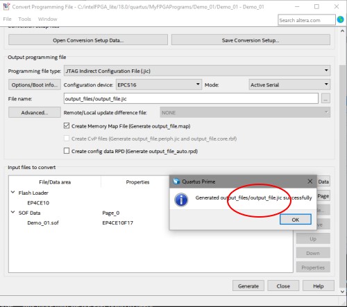
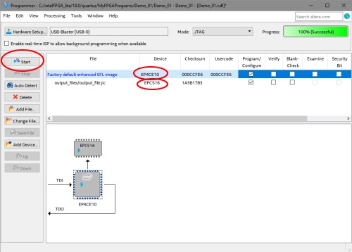
On Intel's own discussion forum are several threads on the topic of solving the "outdated driver signature problem", specifically on how to obtain and install the correct updated driver. This properly solves the issue of device manager not installing the driver for the Blaster, and Quartus not being able to see the Blaster. I too encountered this issue when I first installed Quartus on Windows 10 about 6 months ago, and though the process is a pain to follow it does solve both issues.

On Wednesday, January 26, 2022 at 5:23:27 PM UTC-8 michae...@gmail.com wrote:

Following up on a discussion tonight, I found this helpful to get the USB Blaster running on windows.


Quartus USB Blaster Driver Issues

 Peter Higgins wrote the following directions for situations in Windows where the USB Blaster driver is not recognized.


You first have to disable driver signature enforcement. This is the sequence: 


1 - Go to windows 10 settings and search for "advanced startup options" 


2 - Under Advanced startup, hit "Restart now" 


3 - After a moment, you'll get a "choose an option" screen - choose "Troubleshoot", then "Advanced options", then "Startup Settings" 


4 - You'll get a screen telling you what you will be able to change and a single "Restart" button - press it. 


5 - If your boot drive is BitLocker encrypted, you'll need to enter the recovery key (press return, enter the key in the text box then hit return again - it took me three goes to realize I had to hit return before I could enter they key !) 


6 - You'll be given a menu of options, number 7 disables driver signature enforcement 


7 - When the PC restarts, use Device manager to update the drivers - this time you'll get a warning about the signature, but they install fine. 


8 - When you've finished, restart normally to re-enable signature enforcement.


Henry Broekhuyse pointed out there is an updated driver available from the Intel web site – installation of that driver is the method recommended by Intel’s support people,
with instructions found here
https://www.intel.com/content/www/us/en/support/programmable/articles/000085878.html
The note refers to the “Download Cable II” but it works with all “USB Blasters”.


Adding Modules

One enormous advantage of FPGA's is you can add already constructed "modules" of considerable complexity easily from the web.  Things like UARTs, RAM, ROM, SPI and I2C interfaces, and of course CPUs (e.g. a Z80).  The format can be in
Verilog, VHDL or .bdf format.  If the first two, then you need to make a .bdf module in Quartus first.
Use:
    
     Quartus Adding File
  
Quartus of course supplies basic modules like 74xx TTL chips and common functions found in its "IP library". 
The above video from  ClockFabrick Electronics Academy explains all this.

Adding an FPGA ROM.
You can internally build your own ROM's. A Cyclone IV will allow us room for up to 128K of ROM.  If you are using an 8 bit FPGA CPU (e.g. Z80) loading the .HEX file is simple.
Click on the ROM module and launch the IP Property Editor. Step through the various dialog boxes. Be sure you point the current ROM HEX file to the correct location on your system. Here is an example:
    
     Quartus Adding HEX file
 
Typically your .Z80 or .ASM files will not be in the same directory as your Quartus files. That's OK so long as Quartus points to them.
16 Bit ROMs are more complicated. See an example here.


Burning FPGA Code to Flash RAM

Normally when building/debugging a board the FPGA is programmed via  the JTAG socket on the Waveshare adaptor. The data is lost however whenever the power is turned off.   While fine for code development etc. it is not desirable for a final board configuration.  Like most FPGA applications the "final" code is saved in Flash RAM and immediately loaded by the FPGA each time upon power-up.  This is a standard and common characteristic of most FPGA's. Some older models in fact had a ROM onboard.    Our Cyclone IV Adaptor board has 16MB of Flash RAM on board for this purpose -- way more than we are ever going to need!

The tricky part is programming this Flash RAM.  I found the Intel documentation poor and confusing.  Here is a summary of the process: 
  
Within Quartus you need to "convert" your normal JTAG FPGA .sof programming file to a special file .jic to program the Serial Flash RAM chip on the Weveshare board.

Within Quartus, click on the File Menu and select "Convert Programming files". The dialog box below will popup.
From the dropdown box on the "Programming File Type"  select a .jic file type.
This is the file format that is required to program the onboard serial Flash RAM.
For the Options/Boot info select EPCS16. Leave Active Serial as is.
You can name the .jic output file anything you like. I usually just leave it output_file.jic.
Note it will be in the Quartus generated "output_files" folder within your work directory.

Next click on Flash loader within the lower "Input Files to Convert", then click on the highlighted "Add Device" button.
You will get a popup dialog box as shown below.
Select Cyclone IV  and EP4CE10.  Note Quartus takes some time to allow you to actually select these options -- seems to be doing things in the background!
Next click on "SOF Data" and "Add File".  You should see your "normal" FPGA program .sof file in your "output_files" folder within your work directory.
Finally click the "Generate" button.
You should get a popup dialog saying "Generated output_file.jic successfully.
Note the name and location of the converted file. Then close that dialog box.  See the pictures below.
                      
    Programming 1     Programming 2
 
Programming 3 Programming 4
   
Programming 5
     
Next we need to actually flash the Waveshare boards RAM chip.
Click on the normal "Program Device (Open Programmer)" you normally use. If its not already open,  give it time to come up as a dialog box.
Make sure your board has power.  To be safe click the Auto Detect button. your normal
xxx.sof file should display with the device set as EP4CE10F17.

First delete the above line xxx.sof  |  EP4CE10F17 etc.
Click on Add File and select the xxx.jic file you just generated above.
Click on the Program/Configure little square character boxes.
The chip diagram below should show only 2 chips as shown. If more right click on any 'extra' one and delete it. The dialog box must look as shown below.
The Start button should highlight.
Click on this and you will flash the RAM chip.  Follow the Progress bar until it is done -- it takes about 1 minute.
You can power off and re-power your computer.
Your FPGA board should (after reset), start with whatever FPGA code is within the chip.
  
Programming 8
 
Note when you close the above dialog box, normally you do NOT save the changes.
Typically you want the chip to be quickly reprogrammable.

 
Installing Quartus Lite on Windows.
In spite of its name the
Quartus Lite IDE is a large program.  When fully installed the Quartus folder is over 15GB in size.  Installing it makes Microsoft's Visual Studio seem lightening fast! 
 
That said,  its an excellent IDE.  Figure on 1 hour to install and get it right.  For our purposes we will only be using probably 5% of its capabilities, but I have found if you try and get smart by not downloading or removing sections you run into problems later during usage. 

The Intel Quartus download page  offers a number of download options and versions.  Select the
Lite version, and V18.0, (or later) versions for windows. Just ignore all the individual files etc. and download the complete "Combined Files" package (Quartus-lite18.0.0.xxx-windows.tar).  This is a ~5.8GB file. When downloaded,  you need to unpack it with something like 7-Zip, WinRAR etc. Expand it into a local (temporary) folder and examine the "Components" folder.
It should contain the following files (Note sone file version numbers will change):-
        
   Quartus Install Files  
   
I'm also including it at the bottom of this page in case you have difficulties reaching the Intel download site.

Click on the
QuartusLiteSetup-xx.x.x.xxx-windows.exe program.  Your computer will show the hour-glass icon for almost 2 minutes! Nothing appears to be happening. This I assume is because its unpacking the compressed files in RAM.
Eventually, it gets back to you, with the usual legal/folders questions. After that the whole process is completely automatic/self-contained.  It just takes a long time (~30 min).
Now while you can place your own FPGA files anywhere you like,  if you wish to have a simple setup put  all your FPGA files must be one folder. For example in my case:-
C:\intelFPGA_lite\18.0\quartus\MyFPGAPrograms\Example\

Note, I have located FPGA ROM .HEX files to a sub-folder called \Example\
ROM_HEX_FILES.  If you modify any S100Computers supplied CPU code/HEX files you will need to inform Quartus of the files new location.

During any compile Quartus uses the file
example.qsf to locate ROM hex files (and other things).  Not finding them it would give errors, you have to set your own path.  By having all HEX files as a subfolder everything is self-contained.


Building and Debugging a S100Computers  FPGA program.
There are a number of cross-connected programs you need to have running simultaneously to use or modify the FPGA code provided by S100Computers.
It really helps if you can have all the program windows open on the screen at once.  This is not essential however.  I use a Dell 34" wide monitor which is excellent for this.
Also the Quartus complies are processor intensive. Even with CPU 6 cores it takes the best part of a minute to compile most programs.
Here is a picture of a typical setup.
  
   Quartus Capture 

The main program is of course Quartus. You load the project file (
xxx.QPF) and the actual xxx.BDF file for your board.
Compile this file so its error free.
For many S100Computer boards that contain a ROM in the FPGA you will need to direct Quartus to the location of its .
HEX file. (In the S100Computer downloads its already setup in the supplied .zip file).
But if you wish to change it, you need to let Quartus know its new location by clicking on the ROM to bring up the "
IP Parameter Editor" in the xxx.bdf file.

Next you need to "Burn" the above code into the FPGA. You do this with your USB Blaster (or other device) clicking on the  "
Program Device Option" in Quartus.
Since most boards have a USB Serial TTY output you need to load a TTY terminal to the board. I use Absolute Telnet.  This should display the boards monitor or runtime program.

All boards with an FPGA CPU have supplied CPU source code.  Typically you will be altering the
.Z80 (or .ASM) file during development. 
I use Visual Studio as my editor and the Altair SIMH program to do the assembly. Since this is a repeated process,
Altair has its own window beside the Visual Studio editor.  

Often besides the FPGA Board software there is a "normal" S100 bus operating program to interact with the FPGA board. 
In the example above of a FPGA Disk Controller there is a "normal" S100 bus CPU program to interface with the board. Select drives, show sectors etc.
In the above example this is the second (RHS) pane in Visual Studio,
IDE_DIAG.ASM.
 
Again assembly is a repetitive step so we have a second copy of
Altair SIMH to construct the S100 bus .COM file.
 
Finally we need to get this file from the PC to the S100 system. I use PCGET to do this.
I use the Z80 master "
X" command to load the file into RAM at 100H.
Again I use a second window of Absolute Telnet -- using the File Transfer menu option.  (This is the window at the bottom LHS above).
Then the "
G100" command to run it.

If you are in CPM you can use
PCLOAD.

Finally one trick I use is in the Altair windows: rather than each time typing
SUBMIT FPGA_DC.Z80,  I have a submit file xxx.sub so one can just type SUBMIT XXX
The submit files are always include in the downloads but here is the
FPGA_DC.SUB one anyway:-

R FPGA_DC.Z80
Z80ASM FPGA_DC FH
HEXCOM FPGA_DC
W FPGA_DC.HEX
W FPGA_DC.LST


Quartus File Downloads
Version 18

Quartus-lite-18.0.0.614-windoes.exe.zip                                This is the older V18 .tar version  file 'expanded". (It does not have annoying Intel commercials upon signon)    ( V18  10/18/2022))

Version 21
Quartus-lite-21.1.1.1.850-windows.tar                                  This is a .tar file containing Quartus Lite and support programs from Intel (on 10/19/2022). Note it's almost 6GB in size    ( V21   10/19/2022) 
Quartus-lite-21.1.1.1.850.zip                                               
This is the .tar file 'expanded". Run the file QuartusLiteSetup-21.1.1.1.850-windows.exe to intall Quartus on your PC    ( V21  10/19/2022)


Other pages describing my S-100 hardware and software.

Please click here to continue...

This page was last modified on 10/20/2022