| Jumper |
Function |
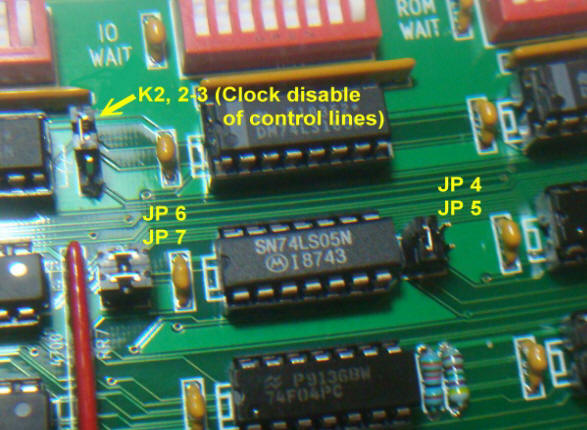
| JP5,JP6,JP4,JP7 |
Used only if the board is
to act as a bus master or are not generated by a front panel board. Generates Power On,
Reset etc. |
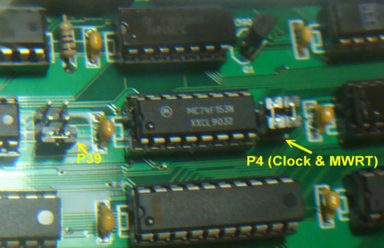
| JP4, 1-2 |
Use only if no other board
generates the S-100 2MHz clock signal when the Z80 is active |
| JP4, 3-4 |
Use only if no other board
generates the S-100 MWRT signal when the Z80 is active |
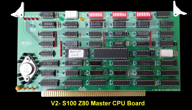
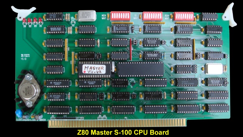
| SW4 (ROM
WAIT) |
Sets number
of wait states for onboard EEPROM (0-8). I use 1 wait state,
so switch 8 (right most switch) is closed, the rest are open |
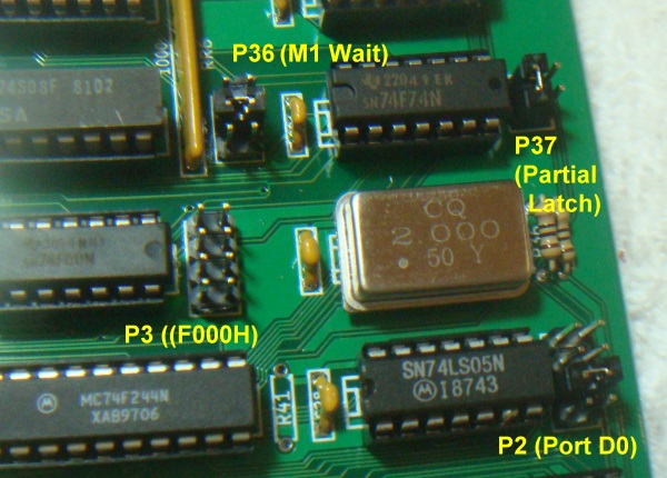
| P36 |
Allows wait states. 1-2,
every sINTA, 3-4, M1 memory bus cycles, 5-6 All Memory
cycles. I use 3-4. |
| SW2 (ME WAIT) |
Sets number
of wait states for P36 options. I use 1 wait state for M1
cycles only, so switch 8 (right most switch) is closed, the rest are
open |
| SW3 (I/O WAIT) |
Sets number
of wait states for port I/O cycles. I use 2 wait states, so
switch 7 & 8 (right most switches) closed, the rest are open
|
| K2 |
Normally set 2-3, however
older pre-IEEE 696 boards (for example the Cromemco dazzler board)
often require 1-2. |
| P37 |
Normally 1-2 (Partial
latch mode). |
| K1, 2-3 |
If NMI software is not
implemented do not connect |
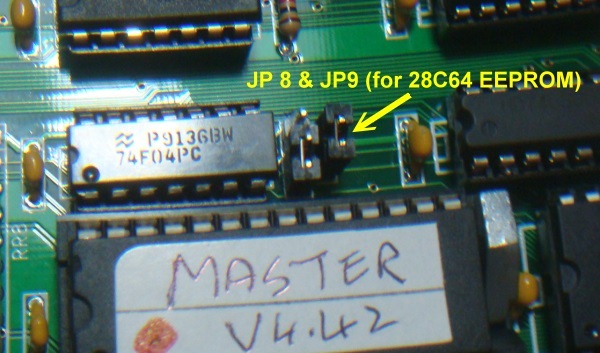
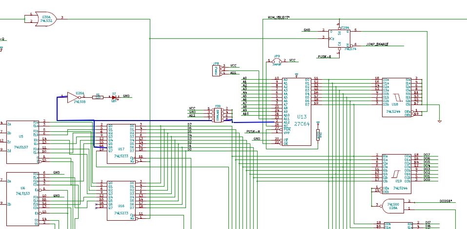
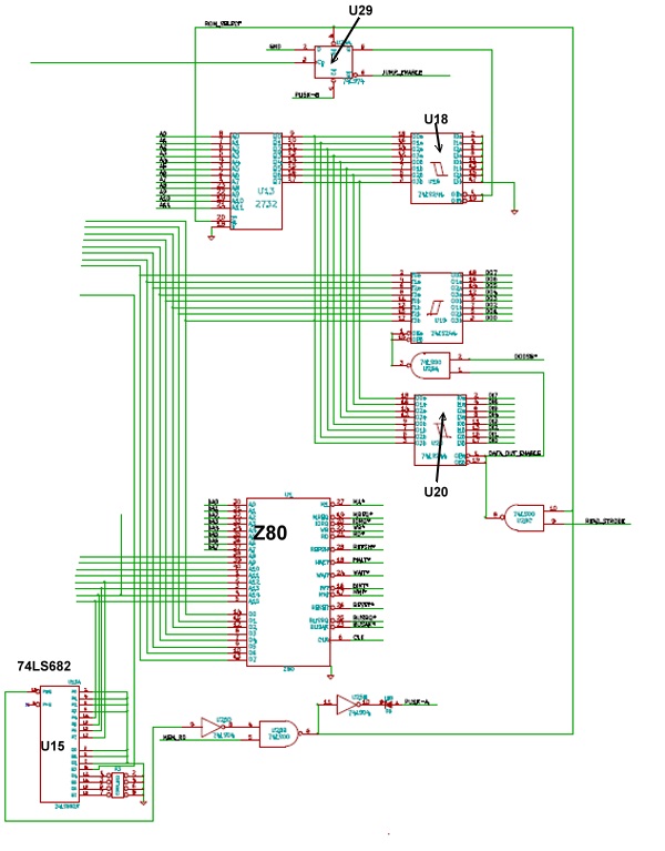
| P39, J88, JP9 |
These jumpers are to
configure different EPROMS and EEPROMS. (For a 28C64:- P39
5-6, JP8 1-2, JP9 closed). |
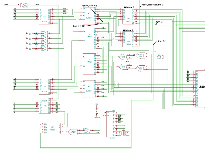
| P2, 5-6 |
Memory window
configuration port. I use I/O port D0H |
| P3. |
No jumpers. This sets the
PROM boot address to F000H. |
| JP1, JP2, JP3 |
This provides extra ground
lines on board IF ALL boards meet IEEE-696 specs. Normally
unconnected. |


.jpg)