A Short History of Microprocessors
The Early Days
The early history of the microprocessor is usually associated with the company Intel and the creative environment that existed in the San Francisco Bay Area -- or "
Silicon Valley" as it is often called. What is not commonly appreciated is that this was no accident, there had been a long and convoluted history of companies and people pioneering electronics firms in the San Francisco region for decades before Intel arose.
One could argue that the industry started back in the 1920's when three guys William Eitel, Jack McCoullough and Charles Litton decided to make radio tubes for their friends in the amateur radio arena having dabbled with radios themselves in the late 1910's. Back then, the Bay Area was a center of Ham amateur radio activity representing over 10% of all the Ham licenses in the country. Indeed a couple of radio companies were actually located there. Because amateur radio utilized higher frequencies than commercial radio at the time, Ham radio tubes had to be of a very high quality -- in particular hold very high vacuums. Word spread about their tubes high quality. The business rapidly grew.
Litton decided to specialize in the manufacture of glass working laths that eliminate the need for tubes to be made by hand and founded the company
Litton Engineering Laboratories. This increased tube reliability further. Eitel and McCollough joined forces to become
Eitel-McCoullough. The two groups produced their first major commercial tube called the
150T. It was an immediate success. Their tubes had lifetimes of 20,000 hours against the norm back then of less than 1000 hours. The start of World War II saw an explosion in demand for tubes from the military. They made numerous high quality power grid tubes and tetrodes during those years.
While Eitel-McCoullough were concentrating on power grid tubes, Litton started working on the new British invention of the time, RADAR. This required the construction of a very unique and difficult tube, called a "
Magnetron". The microwave business really put Litton Industries on the map. During the Korean war they were the first to manufacture pulse magnetrons, radar generating devices required to determine accurately target speed. The company was very profitable, Litton retired from the company. It was sold it to an investment group and is a major corporation today.
Litton had a close relationship with a number of people at Stanford university. In particular he was friends with two brothers there, Siguad and Russell Varian who went on to developed a better microwave device, the "
Klystron". The Klystron had a number of advantages over the Magneton, principally being it produced a more stable frequency controlled microwave. He enchoroughed them to set up their own business (
Varian Associates) in the neighborhood. Litton supplied the glass making machinery. Varian went on to be a highly successful company, starting with Klystron manufacturing but later branching out into many industries. Over time numerous support industries were founded around the above core of electronic professionals in the Bay Area.
The Transistor.Case in point, shortly after the end of the war in 1945, Bell Labs in NJ formed a solid state physics group, led by
William Shockley. While Shockley was born in Britain he grew up in the Bay Area. His group at Bell Labs included
John Bardeen and
Walter Brattain who along with others were responsible for inventing the transistor. Later internal personnel conflicts led Shockley to leave Bell Labs and come back to the Bay Area to head up a division of Beckman Instruments in Mountain View (called
Shockley Semiconductor Laboratory) where he felt there was enough electronic talent to quickly pick up where he left off at Bell Labs. He recruited graduates form Stanford university and got off to a good start with the invention of the
Thyristor. However he became an extremely difficult person to work for -- particularly after he obtained the Nobel Prize in 1956 (along with Bardeen and Brattain).
A group of eight of his employees decided to leave and set up their own company focusing on the transistor. They managed to obtain seed capital from an east coast company called Fairchild Camera owned by Sherman Fairchild in 1957. This was arranged by Arthur Rock - back then, just a young security analyst. Fairchild camera made specialized aircraft surveillance cameras at the time and wanted to get into semiconductors. The founders included
Robert Noyce,
Gordon Moore, and
Jean Hoerni all of whom went on to be legendry in the future. They called the company
Fairchild Semiconductor. BTW, Shockley Semiconductor was purchased by Clevite in 1960, and officially closed shortly after being sold to ITT in 1968.
It's hard to appreciate now, but the early days of transistor technology were difficult. They got their brake when IBM decided to switch to silicon (instead of the then common germanium transistors) for core memories in their military applications for the B-70 aircraft. Hoerni in particular perfected a large scale transistor manufacturing process that launched the company. In time Fairchild Semiconductor dominated the production of planar silicon based transistors. The company in fact became the major revenue source of revenue for the parent Fairchild Camera organization.
In the early 1960's the research group (and independently a group at Texas Instruments in Texas) realized that "microcircuits" could be laid down on silicon wafers. However the parent Fairchild Camera company back east did not want to developed the technology. Worse it was becoming clear that Fairchild Camera was not ploughing money back into Fairchild Semiconductor. The founders concluded that Fairchild was not the best place for them to develop microcircuits. They approached Arthur Rock about setting up another new company. Hoerni and a few others left and founded a Teledyne subsidiary called
Amelco. This was the first of an avalanche of employees from Fairchild Semiconductor. Many others defected and became seed stock for numerous Bay Area microelectronic companies in the early 1960's. Perhaps most notable was
Signetics which was founded by Kattner, Allison and Weissenstern of Fairchild Semiconductor. The financing ($1M), was arranged by Lehman Brothers in NY.
It was not long until it became clear that microelectronics was the future. Signetics perfected DTL devices. These were easier to integrate into circuits than RTL devices. "IC's" of increasing complexity and reliability started to appear.
Fairchild Semiconductor eventually realized they missed the boat. They got financing from Corning Glass in NY along with Corning Glass management, scrapped a RTL logic approach they had in-house and competed directly with Signetics on a price basis. Around this time the DIP IC's was developed by Fairchild Semiconductor. This was superior to the flat "T-packages" used earlier. It gave Fairchild a boost and went on to be the dominant IC packaging format.
At that time Amelco took a different direction, concentrating on linear circuits. These were technically more difficult. Their 709 Op-Amp however put them on the map and became the standard operational amplifier of the era. Jean Hoerni later left Amelco eventually setting up a the IC company
Intersil focusing on MOS technology (watches, calculators etc).
Back at Fairchild Semiconductor in the late 1960's the research group there was in fact the first to start developing MOS integrated circuits. The integrated circuits of the early 1960's were bipolar devices. The simplicity and power reduction of MOS devices rapidly became apparent. However the same old problem arose. Fairchild Camera/senior management did not want to rock the boat. The key research team members became convinced they would get little financial rewards for their work. At this time the financial community had organized in venture capital groups and were hunting down key people to do startup companies in the microelectronics area. One such company was
National Semiconductor. Charles Sporck and Pierre Lamond jumped ship from Fairchild Semiconductor to head up that company. This devastated the Fairchild team and it was compounded by the fact their archrival Texas Instruments (TI) had just come out with a new and better type of digital logic, TTL. This was in essence the last straw for the company. Reorganizations came and went. Noyce had hoped to be CEO but was turned down. He, Gordon Moore and some of their closest friends there prepared to leave.
They approached Arthur Rock who immediately provided them with funding to set up yet another microelectronics company called
Intel. Another Fairchild employee Jerry Sanders left to start up his own company at that time also called
Advanced Micro Devices, Inc. (AMD).
Noyce and Moore focused Intel initially on LSI IC's for memory circuits. They also brought Federico Faggan with them from Fairchild who had perfected new techniques in MOS fabrication using polycrystalline silicon instead of metal gate techniques. Their first memory chip was a MOS based 1101 256-bit static RAM chip. It was TTL compatible and used in devices like printers. They improved on its speed and a year later came out with the 1103 a DRAM equivalent chip. Honeywell used their next generation DRAM chip a 512 bit chip in their early computers. The company was airborne.
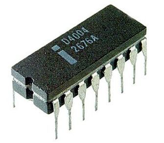
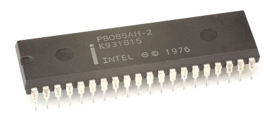
The Intel 4004.In the summer of 1969, Intel was approached by a Japanese calculator manufacturer called Busicom to produce a set of custom chips designed by Busicom engineers for their new line of calculators. They came with their own circuit layout that had designed. It had a number of custom chips, each of which contained about 5000 transistors. A guy by the name of Ted Hoff at Intel was assigned to assist the team of Busicom engineers that had taken up residence at Intel to carry out the project. Hoff looked at the Busicom design and concluded it was way too complex to be cost-effective. Fortunately for them he had worked before with Digital Equipment Corporation's PDP-8 minicomputer, which had a very small instruction set. He reasoned that much of the calculator's complexity could be reduced if they used a small general-purpose processor.
Such a design, using software rather than electronics to do the calculating would be far more efficient and flexible. It did not escape Intel's attention that it would greatly increase the memory requirements of the calculator, but then Intel was in the memory business at that time! Hoff also realized that this processor could be put to many other electronic applications as well. He pitched the idea to senior Intel management who to their credit, gave him the green light to go ahead. The Busicom engineers were still pursuing their original design when Hoff and his group
(in particular Federico Faggin), started work on their new general purpose processor approach. And although the Busicom engineers had simplified their design, each chip still had over 2000 transistors. It would take 12 such chips to make a functioning calculator. Hoff's team figured it would take only 1900 transistors to build his processor. Hoff's general-purpose processor design was chosen over the Busicom design, and Intel got a contract from Busicom to produce the chip that later became known as the famous
4004. Intel's big bang.
Producing the 4004 chip proved to be far more difficult than was earlier anticipated. In those days all lithographic layouts and designs were done by hand. Credit should really go to Federico Faggin for getting chip production going. At that time Intel had only 150 employees most of them operators working in the wafer fabrication and chip assembly lines. The entire R&D organization was about 20 people!
Faggin brought with him two key inventions he made at Fairchild: the
Buried Contact and the
Bootstrap Load that were pivotal in making the 4004. He was at the time one of the few people experience in MOS logic and circuit design and had the crucial knowledge of the then new silicon gate process technology for the above "self-aligned gates". He took the 4004 chip from concept to silicon in just nine months.
At first Intel sold the 4004 exclusively to Busicom, but by the summer of 1971 they realized they had something special on their hands. They negotiated the right from Busicom to sell the chip set to other manufacturers. In November 1971 Intel advertised the 4004 as a four-bit processor that performed 60,000 operations per second. By February 1972 Intel had sold $85,000 worth of chip sets. Management at the company started to realize they had a new focus.
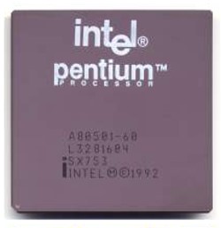
|  |
| | Intel 4004 CPU |
The chip was primitive by today's design, it ran with a clock speed between 740 kHz to at the most 1 MHz. It could execute approximately 92,000 instructions per second and had separate program and data storage areas in RAM. It used a single multiplexed 4-bit bus for transferring: 12-bit addresses, 8-bit instructions and 4-bits of data. It had a total of 46 instructions (of which 41 were 8 bits wide and 5 were 16 bits wide). The register set contained 16 registers of 4 bits each. The datasheet for the 4004 can be obtained
here.
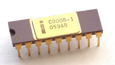
The Intel 8008At the same time the 4004 was being developed, Another company called Computer Technology Corporation, (later renamed, Datapoint) placed bids with Intel and Texas Instruments to design a chip set for a new intelligent CRT terminal they were considering (Their popular Datapoint 3300 CRT terminal was plagued with overheating problems -- too many IC in a small space).
Both companies proposed an 8-bit general-purpose processor. Eight bits, because unlike 4-bits for calculators which work with BCD (binary-coded decimal), ASCII characters require 8-bits. Interestingly as it later turned out, CTC chose neither processor (Intel could not get their chip going in time, TI second sourced the Intel version but it proved buggy). CTC went on in the end to build its terminal with standard logic ICs. Fortunately TI and Intel went ahead with their "8 bit processor projects" anyway. TI focused more on establishing intellectual property in the area initially while Intel quickly blasted ahead upgrading their 4 bit 4004 to the now famous general purpose
8008 "CPU".
The 8008, introduced in April 1972, was the first 8-bit microprocessor on the market. It required at least 20 support chips, but it had 45 instructions that it executed at 300,000 instructions per second, and it addressed a then whopping 16K bytes of memory. That was a lot of memory back then, The 8008 was considerable an upgrade of the 4004. To some extent is was.
| |  |
| | Intel 8008 CPU |
The chip was implemented in 10 micron silicon-gate enhancement load PMOS. Initial versions of the 8008 could work at clock frequencies up to 0.5 MHz, this was later increased in the 8008-1 to a specified maximum of 0.8 MHz. Instructions took between 5 and 11 T-states where each T-state was 2 clock cycles. The 8008 had 3,500 transistors. The chip utilized a single 8-bit bus but required a significant amount of external support logic. It could access 8 input ports and 24 output ports.
Intel's primary goal with the 4004 and 8008 was to replace a large number of discrete IC's with a singe software driven CPU. Few people thought that these chips were suitable for general-purpose computing. At best they were used for "demonstrating computer principles". In 1973 Scelbi Computer Consulting Inc. announced the first general-purpose microcomputer based on the 8008 called the SCELBI-8H. The company was founded in 1973 by Nat Wadsworth and Bob Findley. The 8H came with 1K of RAM and was available either fully assembled or in a kit form, but it never really caught on. SCELBI discovered that they could make more money selling microprocessor software books than hardware and the business switched to highly documented software published in book form. There were a few other attempts; in particular the RGS-008 from RGS Systems and the Mark-8 by Jonathan Titus which was published in amateur-radio publications. They too did not succeed.
That said, the 4004 and 8008 did find good traction in dedicated controller applications. The often mentioned "traffic lights" application is indeed true. The datasheet for the 8008 can be obtained
here.
The Intel 8080
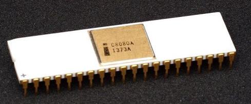
In April 1974 Intel announced the 8080, a significant upgrade to the 8008 that required only six support chips. It had 75 instructions and a tenfold increase in throughput over the 8008. It could addressed a whopping 64K bytes of memory. The 8080 design was proposed by Faggin, but the design team was headed by Masatoshi Shima, a young engineer Intel had wooed away from Busicom (see above). Having learned from the limitations of the 4004 and 8008, the designers made improvements to make their new chip a truly useful computing engine. The 8080 really was the first microprocessor not aimed at simple discrete logic IC replacement. It looked much more like a computer than anything that had come before it, and it was also much easier to use from a hardware standpoint.
| |  |
| | Intel 8080 CPU |
While it was an extended and enhanced variant of the earlier 8008 design, it did not maintain binary compatibility. The initial specified clock frequency limit was 2 MHz and with common instructions having execution times of 4,5,7,10 or 11 cycles. This meant a few hundred thousand instructions per second. It was implemented using non-saturated enhancement-load NMOS, unfortunately demanding an extra +12 volt and a −5 volt supply.
An article in the January 1975 Popular Electronics magazine featured the first in a series of construction articles of a home computer utilizing the 8080 CPU. It immediately caught on and sprung up a whole cottage industry.
See below.
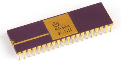
The Motorola 6800 Seeing the success of the 8080's success other major chip manufactures began to wake up. Motorola began working an equivalent chip which they called the
6800. This chip was designed by a guy called Chuck Peddle. Motorola was the first company to introduce a complete line of peripheral chips designed specifically to go with its new microprocessor --thus providing a very integrated hardware solution. These chips included a parallel I/O port chip (the 6820), and serial port chip (the 6850). Motorola also delivered with their chip set a data set manual that became the gold standard for the industry. At $25 a pop everybody had to have one. This probably more than anything else was that book that got many utilizing microprocessors in their hardware designs or as a hobby.
| |  |
| | Motorola 6800 CPU |
This was also the beginnings of the two great microprocessor religions. Intel and Motorola CPU's look at the outside world differently. Intel treats all memory words with the low byte first in RAM then the high byte -- this is called "Little Endian" storage. Motorola places the high byte first then the low byte -- this is called "Big Endian" storage. Assemblers in the Intel world move data/registers right to left. In the Motorola world it's the opposite. Intel treats outputs to RAM and IO ports differently with separate hardware and software instructions. In the Motorola world, IO ports are simply special set aside RAM locations with no unique CPU hardware pins.
BTW, the "microprocessor Endian camps" grew out of the mainframe and mini-computer camps which had grown up previously. The first real "byte" oriented machine was the IBM System/360 mainframe (~1964). This was a "Big Endian" machine. Earlier IBM mainframes like the 7094 all the way back to the 709 (vacuum tubes) were 36-bit whole word only oriented machines. The Data General NOVA series was 16-bit word addressed, and originally used Little Endian byte ordering in the software. They later changed all of their software to big Endian. This was probably because they introduced floating point hardware that used the IBM System/360 floating point representation, which was Big Endian. The DEC PDP-11 minicomputer (but not the earlier PDP-10) was Little Endian as was the follow-on VAX-11. The microprocessor world followed the mini/mainframe computer traditions, Intel went the Little Endian route following the DEC lead, and Motorola went the Big Endian route following the IBM lead.
In the early days (particularly for 16 bit CPU's, see below), Intel tended to designate specific registers to specific hardware/software tasks. Motorola tended to have more registers and treated them all the same. Also in the early CPU's, Intel tended to utilize less silicon compared to the larger Motorola CPU's. Each of the above have their followers and advantages. Zilog followed the Intel model with its Z80, Z8001 etc. series, as did the strange Rockwell PPS-8 or Signetics 2650 CPU's. On the other hand the MOS 6502 (but was Little Endian), Texas instrument TMS9900, National Semiconductor PACE or NS16000 etc followed the Motorola camp. This split exist even today with the IBM-PC/Clones/Windows world and the Apple family.
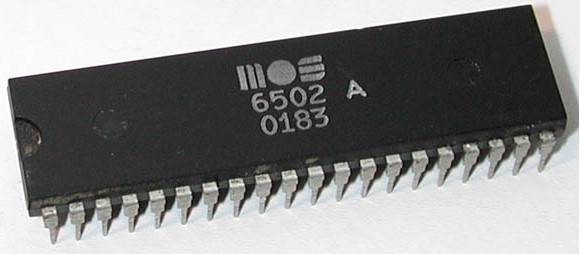
The MOS Technologies 6502 CPUIn early 1975 Chuck Peddle (and a few others), left Motorola and joined a company called MOS technologies. MOS back then was a small semiconductor design and fabrication company based in Pennsylvania. They were setup to provide a second source for Texas Instruments (TI) to provide electronic calculator chips. Once TI started producing their own chips, MOS diversified and became a supplier to companies like Atari, producing for example the single-chip
Pong IC.
The Peddle team got the go ahead to build a new low cost 8 bit CPU. The result was the 6501.
While it was similar to the 6800, by using several simplification tricks in the design, the 6501 could go be up to four times faster. Price was always a big selling advantage for the 6501. MOS simply outperformed others in early working chip yields. (They discovered a way of fixing minor lithographic design layout bugs quickly and easily).
|
|  |
| MOS 6502 CPU |
The 6501, while code incompatible with the Motorola 6800, however it was hardware pin for pin compatible. Motorola sued and forced MOS to make a slightly different chip -- the now famous 6502. A CPU price war started. Intel and Motorola CPUs were at that time selling for greater than $170 each. The MOS chip was one quarter that number. The 6502 would quickly go on to be one of the most popular chips of its day. A number of companies licensed the 650x line from MOS, including Rockwell International, GTE, Synertek, and others. Further improved versions came later for example the 6507 was used in the Atari 2600 or the 6510 for the Commodore 64. Of course the most famous of all utilizers of the 6502 was the Apple.
The Texas Instruments TMS9900
As far back as 1976 TI introduced the TMS9900. It was in fact the first general purpose 16 bit microprocessor and was way ahead of its time in many respects. (There were earlier 16 bits CPU's, for example bit slice logic chips or National Semiconductor's IMP-16 chip set in 1972 or its later one chip incarnation called the Pace. However these were not really general purpose CPUs).
In their wisdom however, Ti never courted the early fledgling hobby PC community and almost went out of their way not to provide support or encouragement to an individual developing a hardware project. Ti's microprocessor focus then was large corporations and industrial applications! Only the Marinchip TMS9900 CPU board was made for the S-100 bus.
|
|  |
|
| Texas Instruments TMS9900 CPU |
The TMS 9900 had a 15-bit address bus, a 16-bit data bus, and only three special internal 16-bit registers. What was unusual about this microprocessor was all its other general purpose user registers (16 in all), were actually kept in external memory. A single workspace register (WP) pointed to the 16 register set in external RAM (each 16 bits wide). While unheard of today for a general purpose 16 bit CPU, this was OK at the time because most static RAM access times back then were faster than CPU register times. The CPU had a simple but powerful instruction set. Fifteen of its 16 registers could be indexed, although it should be remembered these registers were actually in RAM. Interestingly, illegal opcodes were treated as NOP's. Also unusual, Serial I/O was available through address lines. Common today, unheard of back then.
The TMS9900 was however later used in the TI-99/4 home computers. Unfortunately, to reduce the production costs, TI limited the system to just 128 of 16-bit words of the fast RAM that the TMS9900 could access directly. The rest of the memory was 16 KB of 8 bit RAM that was accessible only through the video display controller, which crippled the performance of the TMS9900.
The Zilog Z80
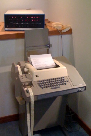 A very typical setup in the mid 70's was an Altair connect to a Teletype printer. The Teletype printer could act as an input device, and you could use the paper tape to save and reload small amounts of code. One thousand bytes of code was a lot in those days! This setup was the basis of CPM's consol IO and data redirection and can be found in monitors like TDL's Zapple Z80 Monitor.