FPGA_DC Board Software
This page contains programs related to the three FPGA_DC Disk Controller Boards. To make any sense you must be familiar with that series of boards before going further.
FPGA_DC.Z80
This is the Cyclone IV specific code to run the Z80 within the FPGA. Please take extreme care in altering the code. Many sections are tightly linked and de[pendent on each other.
Over time new versions of increasing complexity will appear here.
The software for all 3 FPGA_DC boards is fairly complex. There is no way around it, to accommodate the wide verity of cards and disks possible. In theory at least most beginners should not have to alter the software at all. To facilitate the installations all three boards use the exact same software (both within the FPGA and the IDE_DIAG.COM and FDC_DIAG.COM diagnostic programs). In fact the CPM IDE_DIAG.COM will also work with the old IDE/CF board (not of course all menu options). I should also mention that the current software is nowhere near allowing these boards to attain their full capacities. Currently for example only a few Floppy disk formats are covered. The ZFDC Controller Board still currently stands as the better board in this respect. That said, there is no reason why any soft sectored floppy, IDE drive, CF or SD card cannot be utilized by this board. You should have fun modifying the code to do so. I have made a special effort to extensively comment the sections.
Here is how the FPGA_DC.Z80 code is structured:-
Program Equates
Setup Stack and Interrupts
Move the Drive Tables from ROM to RAM
Initialize the IDE Drives and Tables
Initialize the Floppy Drives and Tables
Check IOBYTE Port to see if a jump to the Z80 Monitor is required
Enter the main program Loop (START_CMD:)
Process each Command sent from the S100 Bus
The Commands code
Code to update the HEX LED Display
Code to send Info to the USB Terminal
The Z80 Monitor Menu and code/loop
The Local IDE/CF Card Menu and code/loop
The Floppy Disks Menu and code/loop
Core WD2793 Routines
General software support routines
Core IDE Drive Routines
Real Time Clock routines
Disk parameter tables
Menu strings
ASCII Text/messages
RAM variables (starting at 9000H in RAM).
Remember if you do modify the above code be sure Quartus knows where the new ROM ZFDC.HEX file is located when compiling the ZFDC.bdf file.
The file is at the bottom of this page (Z80 Monitor software for FPGA_DC.ZIP).
The FPGA_DC Diagnostic Programs IDE_DIAG.ASM & FDC_DIAG.ASM
For debugging the IDE and FDC containing circuits of these boards I have written two Z80 programs (IDE_DIAG.ASM and FDC_DIAG.ASM) that reside in the S100 bus RAM at 100H. It assumes the FPGA_DC board S100 IO ports are 80H and 81H and the Console IO is our Propeller Console IO board (ports 0H and 1H). Because they reside at 100H they can be loaded with CPM or you may download it from your PC via a serial link and the Z80 Master monitor X command (X100). By now this process should be familiar to most of our users. There are other ways to do this, but in the end you need to have the IDE_DIAG.COM (or IDE_DIAG.HEX) reside at 100H in RAM and jump to 100H from a Z80 S100 bus monitor. For the FDC circuit boards you need FDC_DIAG.COM (or FDC_DIAG.HEX).
Note if you intend to run the program from CPM before assembly you need to change:-
FALSE EQU 0
TRUE EQU NOT FALSE
CPM EQU FALSE ;TRUE if output via CPM, FALSE if direct to hardware
DEBUG EQU TRUE ;TRUE Show detailed Sector R/W error codes
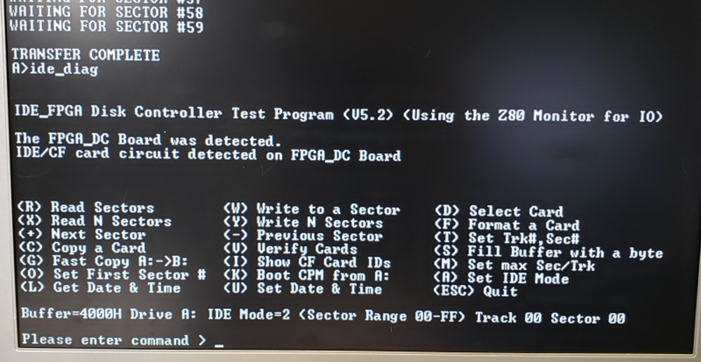
The IDE Circuit Diagnostic will sign on as follows:-
After you select the drive you wish to work with the above menu will appear.
As you can see this is a more elaborate version of the onboard FPGA_DC Board Z80 monitor commands.
Most of these commands are self-evident. A number take one or more follow-on single byte parameters. Some return to the S100 bus one or more single byte values. In all cases they must return the CMD_COMPLETE (F0H) byte value confirming to the S100 bus BIOS that the requested operation completed successfully. Anything else is regarded as an error and the BIOS must act accordingly.
BTW, This program will also work with the old Dual IDE/CF Card S100 Board. Of course some of the menu commands are not functional.
On the
FPGA_DC Z80 monitor side the interpretation of these commands can be quite involved but on the S100 bus side (all the user has to be concerned with in writing a BIOS) it makes things very simple. In fact almost all the commands are one of five commands:-
CMD_SEL_DRIVE EQU 5H ;**** (Re)select an already Initilized drive
CMD_SET_TRACK EQU 7H ;**** This will set head request to a specified track (ONLY)
CMD_SET_SECTOR EQU 9H ;**** This will set sector request to a specified sector (ONLY)
CMD_READ_SECTOR EQU 10H ;**** Read data from the CURRENT sector (on current track,(side),drive).
CMD_WRITE_SECTOR EQU 11H ;**** Write data to the CURRENT sector (on current track,(side),drive).
CMD_INIT_DRIVE EQU 30H ;Select AND Initilized the current drive
Even though its a pain, I have written the code in Intel/8080 format rather than Zilog Z80 format to allow users to easily splice in modules to a CPM BIOS they may wish to build or modify.
All drives are always available. The default drive format is up to 0FFH tracks, 0FFH sectors/track and 512 byte sectors for IDE/CF
Card drives.
These parameters can be easily changed by a "Disk Parameter Table" at the end of the FPGA Z80 monitor code (or by setting bits 1 & 2 of the IOBYTE switch, see below).
For those that have built and used the ZFDC floppy disk controller board they will recognize this command driven approach. However because CF and SD cards are quite different the actual commands and the Disk Parameter Tables are different. The Z80 IX register always points to the start of this table.
Here is the Disk Parameter table for a CF Card Drive:-
IDE_DRIVE_1:
DB CFCARD ;0H, (0FFH), DISK_TYPE (Default IDE Card/Drive)
DB 0FFH ;1H, Default Card Present
DB IDE_CS_1 ;2H, DRIVE_CS, actual Drive CS* Line
; Bits 0,1 are used for drive hardware selection (00=A, 01=B,10=C,11=D)
; Bit 2, 1 if side A is selected, 0 if Side B
; Bit 3, 0 if 8" disk, 1 = 5" disk
; Bit 4, 0 if Single Density, 1 = Double Density
; Bit 5 WD2793 INTRQ 1=ON, 0=OFF
; Bit 6 Write protect flag 0 = ON, 1 = OFF
; Bit 7 Drive Head load (currently unused)
DB 1 ;3H, Drive NUMBER
DB 0 ;4H, INITILIZED, uninitialized
DB 2 ;5H, 512 Bytes/sec flag
DB 0 ;6H, Tracks set aside for operating system (e.g. CPM 2 for floppies)
DB 0AH ;7H, HEX of Drive letter
DB 'A' ;8H, ACCII Character for Drive
DB 0 ;9H, First sector #
DW 512 ;0AH, <------ 512 Bytes/sec
DW 00FFH ;0CH, SECTORS PER TRACK:- (Was 3CH (60)for my on old CPM3 for Kingston CF 8G). (Note. No +1 for cards)
DW 00FFH ;0EH, Max Tracks
DW 0000H ;10H, TRK, Current Track
DW 0000H ;12H, SEC, Current Sector
DB 0H ;14H, Side
DB 0 ;15H, Formatting (Not used for SD/CF cards)
DB 0 ;16H, GAP1 ""
DB 0 ;17H, GAP2 ""
DB 0 ;18H, GAP3 ""
DB 0 ;19H, GAP4 ""
DB 0 ;1AH, GAP4R ""
DB 0 ;1BH, GAP fill byte
DB 0E5H ;1CH, CPM Sector data fill byte
DB 0 ;1DH, Special Flag
DB 0000H ;1EH, Skew Table (Not used for SD/CF cards)
DB 0 ;20H, Format Number
DW 0000H ;21H, Track Size
DB 0 ;23H, Number of (Floppy) disk sides (Not used for SD/CF cards)
DB ' IDE/CF/SD Card A: ',0 ;24H
So the value of Bytes/Sector would be (IX+SEC_SIZE_BYTES), where SEC_SIZE_BYTES = 0AH.
The nice thing about Z80 codes is (IX+RAM_OFFSET) behaves the same as any Z80 register. For example CP A,(IX+RAM_OFFSET) is like CP A,C or LD A,B
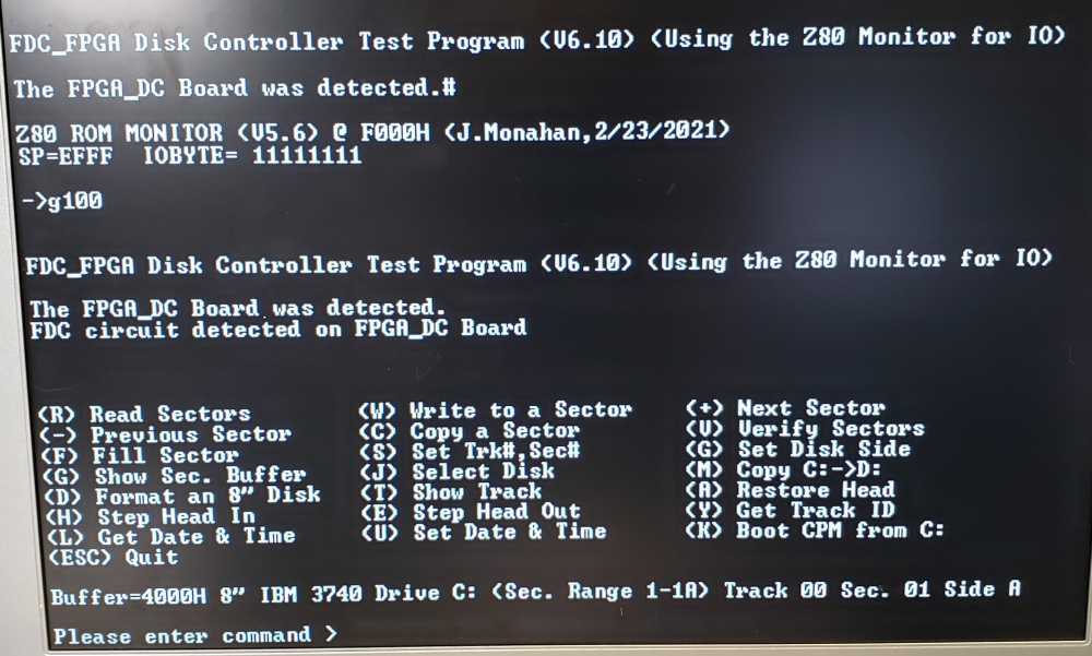
The same type of menu is presented for the FPGA_DC+FDC circuits. It behaves the same way except there are a few more diagnostic tests for the Floppy disk hardware.
Here is how the main menu appears.
Here the Drive tables have more meaning. Here is the table for a 8" Single Density One Sided Floppy disk:-
FL_DRIVE_3: ;(0F0H), 8" SINGLE DENSITY DRIVE VARIABLES (IBM 3740 Format)
DB IBM3740 ;0H, (0FFH), DISK_TYPE (Default IDE Card/Drive)
DB 0FFH ;1H, Default Card Present
DB FL_CS_1 ;2H, DRIVE_CS, actual Drive CS* Line
; Bits 0,1 are used for drive hardware selection (00=A, 01=B,10=C,11=D)
; Bit 2, 1 if side A is selected, 0 if Side B
; Bit 3, 0 if 8" disk, 1 = 5" disk
; Bit 4, 0 if Single Density, 1 = Double Density
; Bit 5 WD2793 INTRQ 1=ON, 0=OFF
; Bit 6 Write protect flag 0 = ON, 1 = OFF
; Bit 7 Drive Head load (currently unused)
DB 3 ;3H, Drive NUMBER
DB 0 ;4H, INITILIZED, Unitilized
DB 0 ;5H, 128 Bytes/sec flag
DB 2 ;6H, Tracks set aside for operating system (e.g. CPM 2 for floppies)
DB 0CH ;7H, HEX of Drive letter
DB 'C' ;8H, ACCII Character for Drive
DB 1 ;9H, First sector #
DW 512 ;0AH, <------ 512 Bytes/sec
DW 00FFH ;0CH, SECTORS PER TRACK:- (Was 3CH (60)for my on old CPM3 for Kingston CF 8G). (Note. No +1 for cards)
DW 00FFH ;0EH, Max Tracks
DW 0000H ;10H, TRK, Current Track
DW 0000H ;12H, SEC, Current Sector
DB 0H ;14H, Side
DB 40 ;15H, HEADER GAP (SD-Systems has 100-27, IBM is 40!)
DB 6 ;16H, GAP 1 (0's)
DB 11 ;17H, GAP 2 (FF's)
DB 27 ;18H, GAP 3 (FF's)
DB 247 ;19H, GAP 4 (FF's)
DB 1 ;1AH, GAPR (Flag for multiple repeats of GAP4)
DB 0FFH ;1BH, GAP Format fill character
DB 0E5H ;1CH, CPM Sector Data Fill Character
DB 0 ;1DH, Special Flag
DB SKEW_IBM ;1EH, Sector Skew Table location
DB 0 ;20H, Format Number
DW 13F0H ;21H, Track Size
DB 2 ;23H, Number of (Floppy) disk sides
DB ' 8" IBM 3740 Drive C: ',0 24H
Note the very specific values used to format a track. (The floppy disk format routines were the most tricky to write in the FPGA_DC.Z80 code. Do not change these values unless you know what you are doing).
The advantage of the command driven approach is that the current S100 bus CPU does not have to go into DMA mode or sync the bus with wait states when reading or writing sectors. Any of our S100Computers CPU boards, in fact in theory, any manufactured CPU board, should work in this system. The downside is that disk access is a little slower. Not as slow as you might think however because while the requested sector parameters are passed back and forth with above commands and handshaking, the actual 512 bytes of data transfer across as a block over the connecting bridge port one byte immediately after the other using the Z80 block IO instruction. Normally you will notice no difference with say a few sectors moved with CPM or even MSDOS. However a total disk copy from one drive to another will be slow. The monitor in fact has a special disk copy command to help with this (CMD_DRIVE_COPY EQU 43H) a little. Remember these CF and SD cards have an enormous capacity -- way outside early days CPM or MSDOS. Copying the first few "tracks" usually is all that is required.
For those that wish to play around with the software there is 512K of RAM available to the Z80 FPGA. Some fancy sector caching routines could be implemented.
Also for MSDOS, multiple sectors could be written or read with a single command. If you develop code improvements please let me know.
The diagnostic programs can be downloaded from the bottom of this page.
Please note there is a CPM
EQUATE
at the start of the
IDE_DIAG.ASM
and FDC_DIAG.ASM
programs which determines how the console I/O is handled; Direct via the
Propeller Console IO Board of via CPM BIOS
calls.
For the former the programs should be loaded into RAM at 100H (via
XMODEM etc.). For
the CPM version they should be moved to a Disk/CF card via
PCGET.
Also for CPM PIP.COM
change the names from
IDE_DIAG.COM and
FDC_DIAG.COM to IDE$DIAG.COM and
FDC$DIAG.COM
Switching Drives and Drive Tables
The default hardware floppy disk drive configuration for the supplied FPGA_DC.Z80 software is:-
Drive C:- 8" IBM 3740 Drive C: (128 Bytes/Sec), a
Double sided disk, 26 Tracks/side.
Drive D:- 8" IBM 3740 Drive D: (128 Bytes/Sec), a
Double sided disk, 26 Tracks/side.
Drive E:- 8" IBM System 34 Drive E: (256 Bytes/Sec), a
Double sided disk, 26 Tracks/side
Drive F:- 2.5" IBM 1.44MB Drive F: (512 Bytes/Sec), a
Double sided disk, 80 Tracks/side
You can access side A and side B
separately of each disk in your BIOS software with the Disk Drive Port select byte.
DB FL_CS_1 ;2 DRIVE_CS, actual Drive CS* Line
; Bits 0,1 are used for drive hardware selection (00=A, 01=B,10=C,11=D)
; Bit 2, 1 if side A is selected, 0 if Side B
; Bit 3, 0 if 8" disk, 1 = 5" disk
; Bit 4, 0 if Single Density, 1 = Double Density
; Bit 5 currently unused
; Bit 6 Write protect flag 0 = ON, 1 = OFF
; Bit 7 Drive Head load (currently unused)
You select the drive with:-
LD A,(IX+DRIVE_SC) ;DRIVE_CS, IX offset=2
OUT (DRIVE_PORT),A
Bit 2 in A determines if you are accessing the Disk Side A or B.
Bits 0 and 1 select the actual floppy drive
So if you have or want to only use a one sided disk you always leave bit 2 = 1. No changes to the
FPGA_DC.Z80 ROM code is required.
If you want to change the disk format of any of the above disks however you must alter the Disk Drive Format tables.
It is easy to do so, but, you must reassemble the .Z80 code and point Quartus to the
location of the new .HEX file before compiling a new .BRD file.
Unlike the ZFDC Floppy
Disk Controller Board the FPGA_DC.Z80
software currently has the disk tables in ROM and does not have code to
dynamically change them after they are moved to RAM on bootup.
This could
be done but it is a tricky task requiring a few new FPGA_DC Board COMMANDS.
Since it will be rarely done I decided its easiest to just change the ROM table
code.
The critical (and extremely hard to find) disk format values can be
obtained from the ZFDC Floppy Disk Controller code
here, (ZFDC.Z80).
Remember the actual table structures are different for both boards. Use
the ZFDC.Z80 table info to
modify values in your FPGA_DC.Z80
file table.
Finally, the actual drive connections can be changed around by changing bits
0 & 1 of DRIVE_CS
in the tables. If
you have only one 8" drive for example you can set
DRIVE_CS to FL_CS_1
for C:, D: and E:
Likewise you could hookup a 5" floppy disk to D: adjust
the table and off you go. Again use the
ZFDC.Z80 table for format info.
For the FPGA_DC Disk tables provide, I assume only one 8" Drive and one 3.5"
drive. I have bits 0 and 1 of
DRIVE_CS = 00 for the drives C, D and E.
and 11 for drive
F.
You can have up to 4 separate drives (00, 01,
10 &11) in the hardware (See the schematic
U23 &U24).
The default CPM3 BIOS assumes only a Single Sided Single Density IBM 3740 disk
for two drives 00 and 01,
(or if you have only one drive, 00 and 01).
It assumes one 8" IBM System 34 DS DD disk can also be in that one drive
(instead of an IBM 1370 disk). It assumes one 3.5" 1.44MB disk is in
Drive F:
This is about as simple a 4 drive setup you can have. Clearly more complex
systems can be setup. You just need to adjust the FPGA_DC ROM tables and
the CPM3 BIOS Disk Parameter table.
Double Sided Disks with CPM.
Unlike MSDOS, CPM3 does not specifically utilize the concept of disk heads or
floppy sides. We get around this by doubling the number of sectors
on a track in the CPM3 Disk Parameter Table.
Any sector number over that defined for a single sided disk track is assumed to
be on the B side of the disk. For example the 3.5" 1.44MB disk
F: has sectors numbered 1 to19 on a track. Any sectors from the BIOS numbered 20
to 38 are assumed to be on the B side of the disk with the same track number.
The code in the FPGA_DC Z80 ROM takes care of all this side switching completely
transparent to CPM3's BIOS. As far as the CPM BIOS is concerned each 1.44 MB
disk track has 38 sectors.
You can of course "force" a B side selection (for example with MSDOS) using the
CMD_SET_SIDE command.
Finally the FPGA_DC
code is intelligent enough to check the disk format and make sure sectors are
not out of range etc.
Running CPM3 from the FPGA_DC Board
One of the initial requirements I laid down in the design of these boards is that one could immediately boot any version of CPM3 that ran on the old Dual IDE/CF card S100 board immediately and unchanged. This is for the FPGA_DC+IDE and FPGA_DC+IDE+FDC Boards. (Clearly not for the FPGA_DC+FDC Board). This considerably increased the complexity of the FPGA code. Particularly tricky is the utilization of FPGA Interrupts to display the Drive, Track and Sector LED displays which are very different on the FPGA_DC Board.
If you have a working Dual IDE/CF card S100 board CF card with CPM3
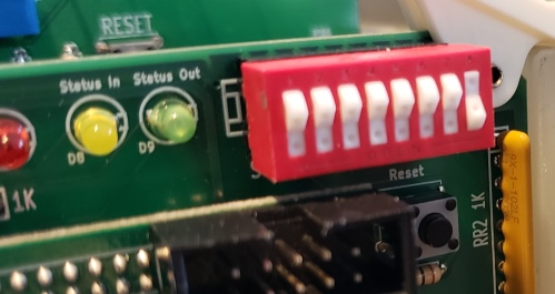
(or MSDOS), on it go right ahead and boot the OS. It should come right up. Be sure you have the IOBYTE switch set as follows:-
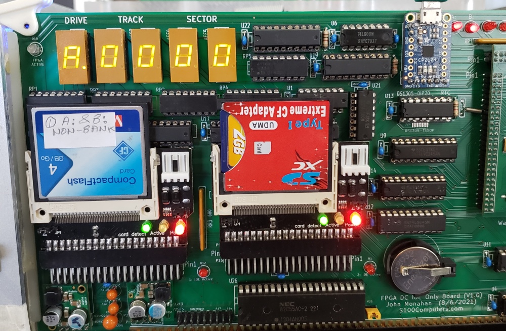
Here is what my very basic two IDE Drive Non banked CPM3 system looks like on boot up (Z80 master "P" Menu Option)
To fully utilize this board and CPM3 you need to be familiar with writing a CPM3 BIOS. Please see here
CPM3 HDISK BIOS Software
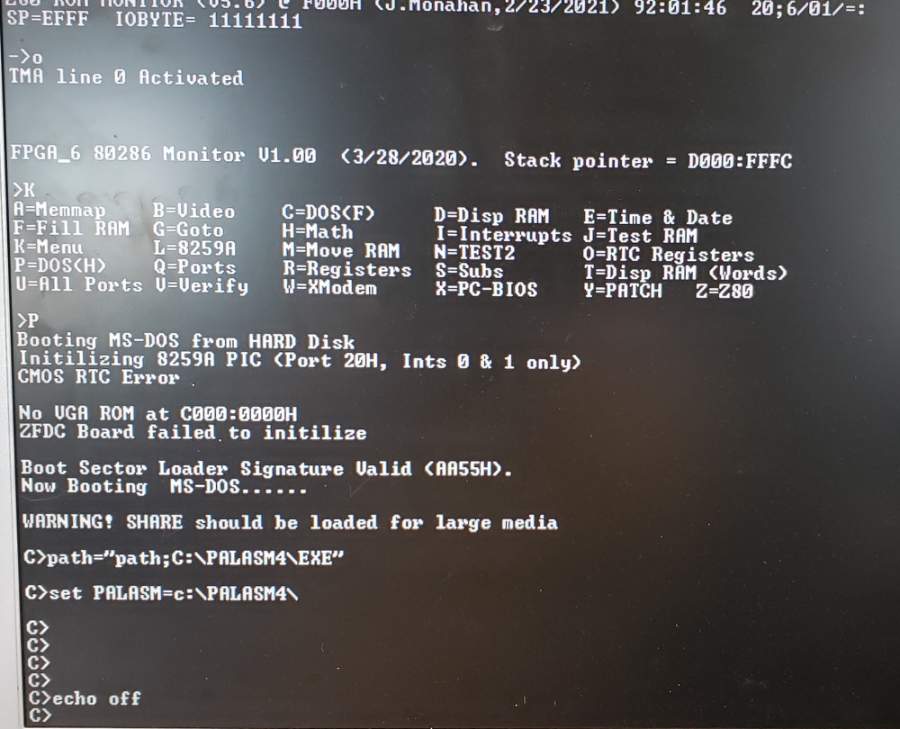
Here BTW, is the corresponding boot of MSDOS from one of our 80286 Boards.
Remember for MSDOS the CF card needs to be in the B: Drive slot (using the default S100Computers 8086 Monitor).
Writing a CPM3 BIOS from the FPGA_DC+IDE Board.
As I said above, if you have a working Dual IDE/CF card S100 board CF card with CPM3 on it go right ahead and boot the OS. For those that don't have a running CPM3 Operating system and/or the Dual IDE/CF card S100 board I provide here a very simple two IDE cards (A: & B:) Non-banked CPM 3 system to get you started. The only other requirements are free RAM from 0H-0FFFFH and a the Propeller Console IO board, or any other Console IO board with ASCII status and data on IO ports 0 & 1H.
You should very carefully read about setting up a CPM3 BIOS here first.
We need to do the following:-
1. Write a CPM program (HSYSGEN.COM) that will write a CPM3 "Boot loader" to a few of the first sectors of a CF card (disk) starting on Track 0, sector 1
2. Write an CPM program called CPM3.SYS that is the core of the disk operating system and place it in the data section of the CPM disk.
3. Add a number of other runtime programs to this same disk including one called CCP.COM.
I will supply a CF card image (below) that allows you to make a fully functional CPM3 OS immediately.
You can then enlarge upon the above CPM3.SYS to make more elaborate CPM3 arrangements incorporating other hardware features. Essentially you replace the file CPM3.SYS with another (larger) one.
To recap then, there are two processes: Making a functional CPM3 CF card to boot CPM for our FPGA_DC+IDE card. Second, modifying that CPM3 to add more functionality to an already running system.
Warning: Be
absolutely careful where you
place the CPM BIOS files and support programs. There are a number of
Windows directories each with similarly named files.
Often these files are different in each directory. It is
essential they you not get them messed up in a different directory.
If in doubt start with a new download.
Making a Functional CPM3 CF Card for the FPGA_DC+IDE Board
This gets around the chick and the egg problem of having a functional CPM3 disk OS to make an OS. We will just download an image I made and "burn' it into a CF card. Put it in the IDE adaptor slot and Boot!
There are a number of ways this can be done. I have formatted a CF card for CPM3 and added the Boot loader, CPM3 and CCP.COM. I have also added a number of other common/useful files to get people started. I have use the program called HDD Raw Copy Tool to make a file containing an exact sector by sector disk image of the card. The program can be found here. It can also be found at the bottom of this page. The image file is called FPGA_DC_CPM_IMAGE.IMGC. Its a large 6.6GB file (since it's a sector by sector copy of the CF card).
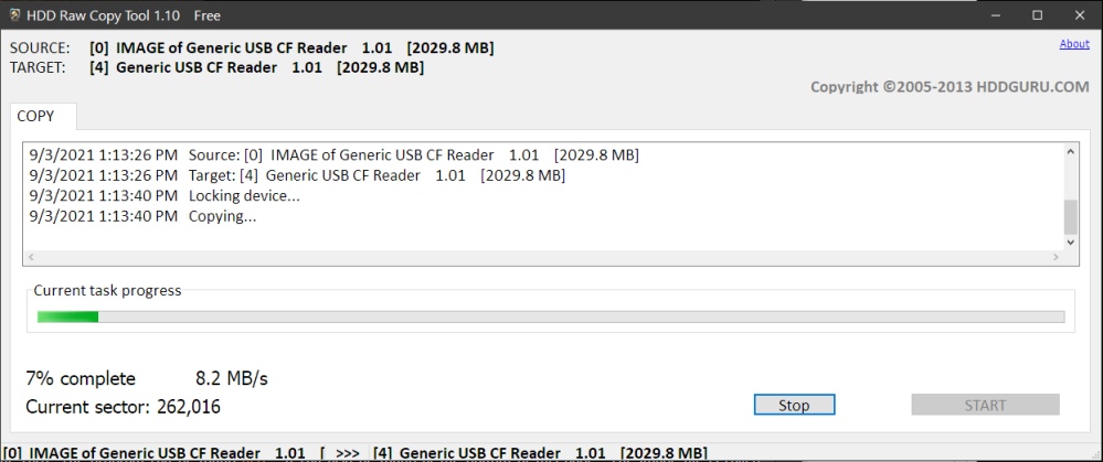
You can use HHD Raw Copy to unpack the FPGA_DC_CPM_Image.imgc on to a CF card (of at least 4GB) on your side. Actually since our CPM3 disk is only 0FFH tracks, 0FFH Sectors maximum, you can probably stop the unpacking process after sector 0FFFFH (65,535). Here is how the "unpacking" dialog looks:-
I should point out the above image file is NOT the same format as the well known CPMTools disk .img file. You cannot us that package to manipulate the CPM files in the image.
If you have a Propeller Console IO board, the Z80 CPU board with the Master monitor and 60K of RAM you should be able to boot up CPM3 on the FPGA_DC+IDE board with the master "P" command
immediately. Other hardware situations can probably be hammered into shape. The only CPM BIOS requirement it the Console I/O ports at 0 and 1.
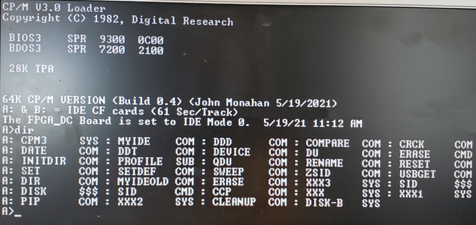
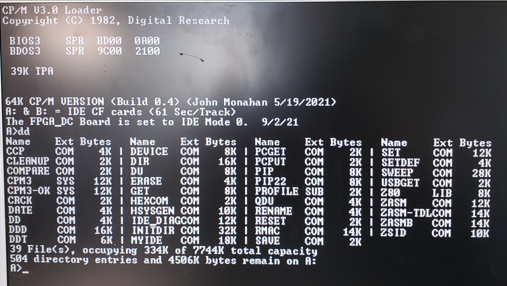
This is how CPM should Signon for FPGA_DC_CPM_Image_2d.imgc:
As you can see the disk has some of the commonly used CPM3 programs.
Normally (for speed) you would have the FPGA IOBYTE switch open. If you close bit 0 (SW1,0) upon boot you should see the following display:
Above you see the CPM3 Boot loader being read in from Track 0.
The IDE_DIAG.COM program is on this CF card. You can use it to analyze the disk itself.
The first thing you should do is make a copy of the CF card (disk) in the B: drive slot. Try and use the same type of card. I found that some older small capacity cards behave strangely.
Always format a CF card with a FAT structure in windows before using it here.
You must then erase the card under CPM before using it, (ERASE B:*.*), because the MSDOS FAT sector fill character is not E5's.
You can use the FPGA_DC Board monitor to fast copy A:->B:, or the IDE_DIAG.COM program to do so. However its usually faster just to use
PIP B:=A:*.*[v] followed by
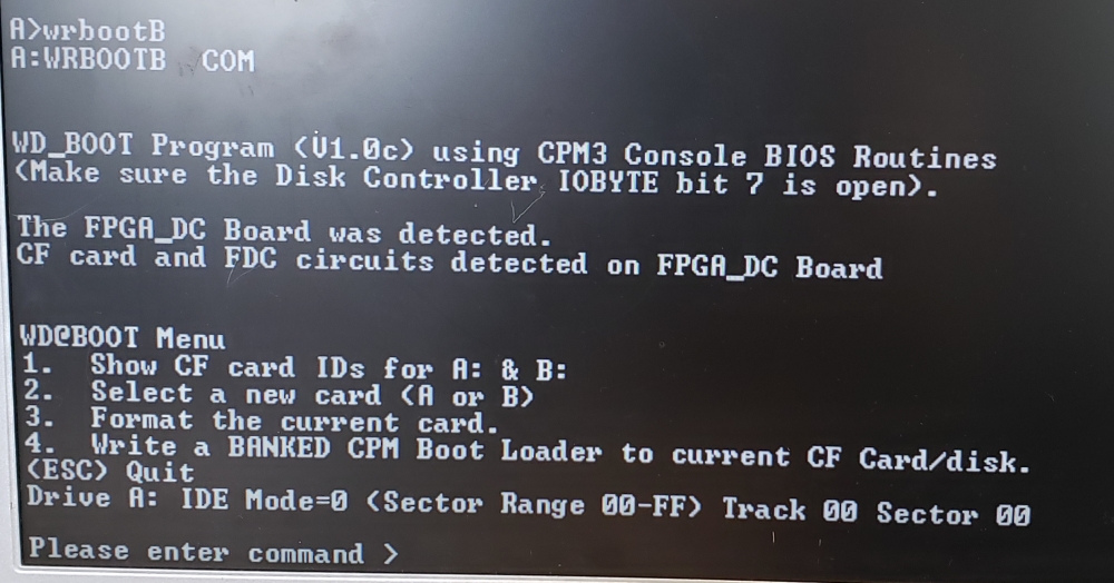
WRBOOT.COM or (for a
banked system) WRBOOTB.COM (selecting drive B:), to make a bootable disk.
CF cards are getting harder to find these days. Try and get the 4GB Verbatim ones. I have problems with some small size lesser known brands.
I recommend you quickly switch over to using SD cards using a CF->SD adaptor. They are way more common and seem faster. Again use 2 or 4GB cards.
Here is a typical setup to making a bootable SD card:
Adding More Functionality to a CPM3 CF Card for the FPGA_DC+IDE Board
Now comes the fun part. The above CPM3 system is about the most minimal system you can use. You will want to add floppy drives (with our FPGA_DC+IDE+FDC board), perhaps other drives, speech
synthesizer, printers, and most important of all -- a banked version of CPM3. The nice thing about CPM3 is the only thing you have to change is CPM3.SYS on the boot drive.
Normally one makes CPM3.SYS on a windows PC using SimH (and here). I will describe this in a moment, but during software development you may find yourself writing version after version of CPM3.SYS to get it debugged. You need a quick and easy way to get the file to your CPM boot disk. There are a number of ways to do this. Elegant, such as updating the FPGA_DC_CPM_Image.imgc directly and using a new CF card each time. However the fastest way is just to transfer the CPM3.SYS file from your PC to the S100 system over a serial connection using a stripped down
XModem program I wrote called PCGET.COM (which is one of the programs on the above CF Card).
You need a functional serial port to do this and a XModem capable program on your PC. This is described here.
I have described elsewhere in some detail how to make versions of CPM3.SYS.
The complete folder for the above A: and B: drive system can be downloaded from here:-
AB Drives Only Zip
It contains
Altair.COM the SIMH program to do everything.
You need to study the .ASM files. The FDC_DC BIOS disk file for example is
HIDE3.ASM.
The good news is the whole CPM3.SYS
construction process is done for you with the batch file called
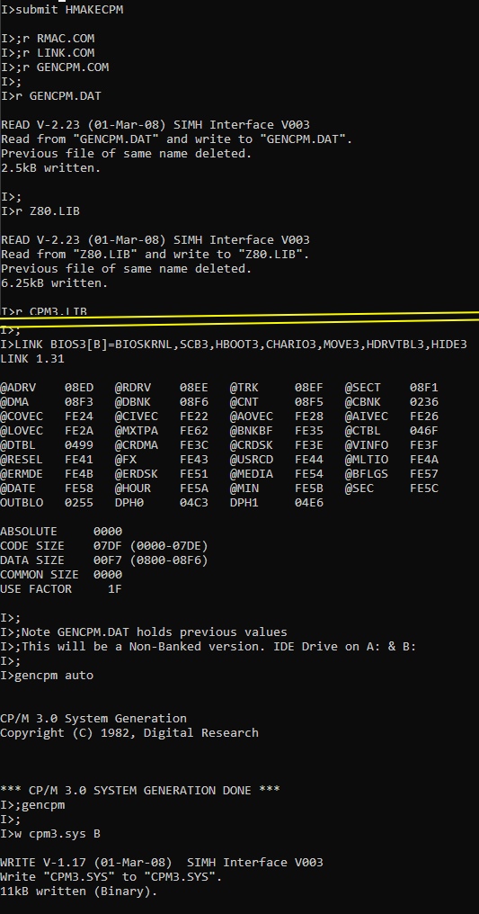
HMAKECPM.SUB
Here is part of the working display:
It is that CPM3.SYS file you need to get across to your CF card from the
Altair.COM containing directory on your PC.
There is one other set of files you may want to have. It's the source files for
WRBOOT.COM -- the program to write the boot image on your CF Card.
Exactly the same process is involved except this time you would move across
WRBOOT.COM with PCGET.
The complete folder for
the old HSYSGEN (non Banked version) can be downloaded from here:-
HSYSGEN.Zip.
Recently I have replaced HSYSGEN
by a new program called WRBOOT.COM
or WRBOOTB.COM
(for the banked CPM3 version). This program is menu driven with more
options.
| |
 |
The file folders can be downloaded from the bottom of this page.
All CF Card images can be found in the
CF Card Images Page
Please click on that page for the hardware setup you need.
FPGA_DC Board Software
Downloads
Z80 Monitor software for FPGA_DC.ZIP .ZIP
File
This is the Z80 code used in the ROM for all 3
FPGA_DC Boards + DC_DIAG
(V2.00
12/19/2021)
Z80 Monitor software for FPGA_DC.Z80 Visual C .Z80 (Text) File
(V2.00 12/2/2021)
IDE_DIAG.ASM Source Code ZIP File
(V5.5 12/2/2021)
IDE_DIAG.ASM Source code .ASM (Text) File (V5.5
12/2/2021)
FDC_DIAG.ASM Source Code .ZIP File (V6.4
12/2/2021)
FDC_DIAG.ASM Source code .ASM
(Text file) (V6.4 12/2/2021)
Write_Disk_WRBOOT code ZIP file of folder of files to make WR_BOOT.ASM
(10/23/2021)
Write_Disk_WRBOOTB code ZIP file of folder of files to make WR_BOOTB.ASM
(10/23/2021)
HHD RAW Copy Tool (.exe install file from
https://hddguru.com/software/HDD-Raw-Copy-Tool/)
A Drive Non-Banked
Folder ZIP
All files required to construct the CPM3.SYS file (10/26/2021)
AB Drive Non-Banked
Folder ZIP
All files required to construct the CPM3.SYS file (10/26/2021)
AB+CDEF Non-banked Folder ZIP
All files required to construct the CPM3.SYS file (10/26/2021)
AB Drives Banked Folder ZIP
All files required to construct the CPM3.SYS file (10/26/2021)
AB+CDEF
(FPGA_DC+ZFDC) banked Folder ZIP All files required to
construct the CPM3.SYS file (10/26/2021)
AB+CDEF Banked Folder ZIP (My main System) All files
required to construct the CPM3.SYS file (10/26/2021)
Write
Non Banked BOOT Loader
All files requred to place the CPM3 Non banked Boot Loader on a CF card
(10/26/2021)
Write Banked BOOT Loader
All files required to place the CPM3 banked Boot Loader on a CF Card
(10/26/2021)
Old HSYSGEN. ZIP
All files required to place make FSYSGEN.COM (10/26/2021)
FPGA_DC_CPM_Non-Banked_2D (1. Universal 2 Drive System).imgc Sector image of a
2 CF Card Drive Bootable CPM3 on a 4GB Verbatim CF Card (1/23/2022)
FPGA_DC_CPM_Non-Banked_6D (2. FPGA_DC+Floppys).imgc Sector image of
a 2 CF card Drive + 4 Floppy Disks Bootable CPM3 on a 4GB Verbatim CF Card (10/20/2021)
FPGA_DC_CPM_Non-Banked_1D (3. One Drive system).imgc Sector image of
a one CF Card Drive Bootable CPM3 on a 4GB Verbatim CF Card
(10/20/2021
FPGA_DC_CPM_Banked_2D (4. Basic FPGA_DC System).imgc
Sector image of a 2 CF Card Drive Bootable Banked CPM3 on a 4GB
Verbatim CF Card
(12/19/2021)
FPGA_DC_CPM_Banked_2D+4F (5. My Main System).imgc
Sector image of
a 2 CF Card Drive + 4 Floppy Disks Bootable Banked CPM3 on a 4GB Verbatim CF Card (12/19/2021)
ZFDC_CPM_Banked_7D (6. Old ZFDC System).imgc
Sector image
of a 2 CF Card IDE Drive +ZFDC Board Floppies Bootable Banked CPM3 on a 4GB
Verbatim CF Card (12/19/2021)