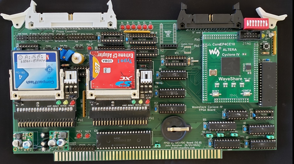
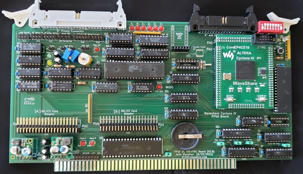
A FPGA Disk
Controller
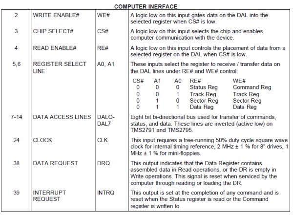
S100 Bus Board
Introduction.
Let me say first --
this are not an easy boards to build! I spent over a year on it with some
different 8 hardware prototypes. The Z80 assembly language is over 8000
lines of Z80 assembly code! The difficulties are not due to complex
FPGA/electronic circuits but rather the large number of possible
software and hardware configurations. The "final" board should be the
last S100 bus disk controller you should ever need! It will handle
most IDE hard drives, most CF cards, most SD cards (with adaptors min & max
sizes). Almost all 8" floppy disk formats (Single & Double Density, Single
and Double Sided). Almost all 5" Floppy disks and 3.5" floppy disks.
In fact the only floppy disk types not covered are hard sectored Northstar
and Micropilis disks. Examples of a CPM3 BIOS are added for some
common disks and formats. In all cases the approach is to vastly
simplified the CPM3 BIOS by having it issues simple one byte commands to the
40mHz Z80 CPU within the FPGA on the board. This controller handles
all disk access including initialization, sector read writes etc. Except for
some tables within the CPM3 BIOS, CPM3 has no knowledge of the disk hardware
-- nor does it care to! Everything is taken care of by this FPGA Disk
controller board.
The early board prototypes started life as self contained S100 bus single
board computers. Indeed this one board in the bus could in theory boot up
and run CPM. This was the basis of molding the system into a
relatively complex hardware setup to present the onboard disk hardware to an
external S100 bus master (or slave) CPU. The bridge
between the onboard drives/software and the "external" S100 bus is via two
S100 bus 8 bit bidirectional data ports. Everything on the S100 bus
side goes across this I/O port bridge. There is no DMA, no S100 bus
wait states etc. This command driven approach makes for very simple
disk operating system BIOS's and is of course completely CPU independent.
In one sense this board is a combination of the hardware on our "IDE
Disk Controller board" first released back 2009 and our
ZFDC Floppy Disk Controller first
releases back in
2010. Well over 400
of these boards have been distributed worldwide! Instead of
using a traditional GAL or Z80 CPU, we utilize an Intel Cyclone IV
FPGA. A Z80 CPU emulator within the FPGA (running at speeds up
to 40MHz) handles all the software. In particular at this speeds
floppy disk sector access is so fast as to be able to read even Double
Density Floppy disk sector data "on the fly" without DMA/wait states etc.
Unfortunately all this comes at a cost of some considerable complexity.
Realizing that many of our members are new to FPGA's I have decided to
present this board in 3 different formats of increasing complexity. In
all 3 cases the same Waveshare FPGA module is used and the exact same
software is utilized.
The boards are:-
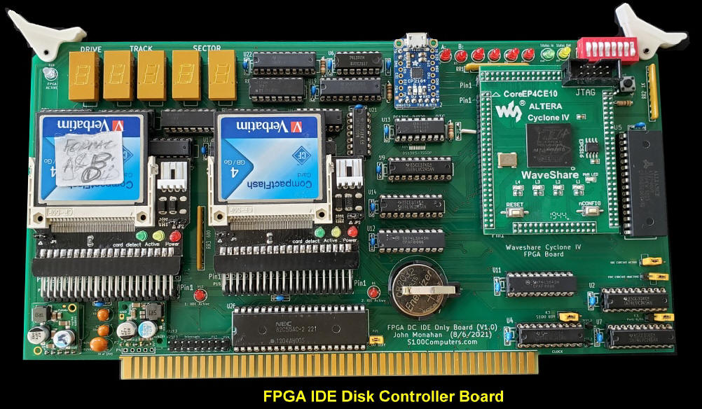
FPGA_DC + IDE Board. This board is in essence an FPGA
driven version of our IDE/CF
Card
Disk Controller board It can be configured into 3 different hardware
"modes" (See below). To help get people started it has a
default mode (Mode 0), where it behaves exactly like the IDE/CF Card Disk Controller
board. In this way you can boot any IDE/CF card version of CPM3 directly
from this new FPGA Board unmodified.
(This unfortunately raised the complexity of the board and its software
considerably and caused me a lot of headaches initially!).
In this mode the actual sector read and writes are done directly via the
S100 bus with the 8255A IO Chip. Any "old" IDE/CF card BIOS does not
know it is talking to a new disk controller. However the FPGA DC Board
actually initializes the IDE/CF card hardware before transferring control to
the S100 bus. A second initialization by old BIOS software does no harm
but actually is not required. The actual sector R/W routines are very
simple (and fast), but are not single byte "command driven" as
the board is really setup for. This mode is there to get users quickly
started with a working disk system. As an extra, a 5 segment LED Hex display
always shows the current Drive, Track and Sector. Another mode (Mode
1), allows the IDE/CF/SD Cards to be accessed in a simple one byte command
driven approach.
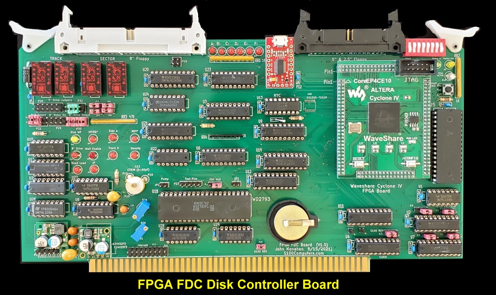
FPGA_DC + FDC Board. This board is in essence an FPGA
driven version of our ZFDC
Controller Board This board interfaces the Western Digital
2793 Floppy Disk Controller to a Z80 emulator within the Cyclone IV FPGA.
The Z80 runs very fast -- for the core disk sector data transfers 40MHz, so
the CPU is not the rate limiting step and so can run in a simple chip status
mode without DMA or wait states. Utilizing the disk parameters table driven
approach of the ZFDC board, any 8", 5" or 3.5" disk format can be
easily utilized. Again understanding what is going on is fairly complicated
but this time the board is completely byte command driven as was done for
the ZFDC Board. Again a CPM3 Single Density Single Sided 8" disk
should boot unchanged with this board. As for the ZFDC board, a 4
segment LED Hex display always shows the current Track and Sector.
FPGA_DC + IDE + FDC Board. This board is a
combination of the two above boards. Needless to say it is much more
complex. For beginners in particular I highly recommend you start with
the above two boards first. BTW, the same FPGA software is used for all
three boards.
Two jumpers on each board redirects the FPGA to the relevant circuits.
Finally all three boards contain a Clock/Calendar chip which can be utilized
by a CPM3 BIOS to time stamp files.
I will now go through a detailed description of each board and its build
process.
FPGA_DC + IDE Board
In a certain sense this is the simplest board. For one, there is
no disk signal adjustments or a multitude of different disk formats to deal
with.
If you are not familiar with FPGA's you need to read up on them. We have
used them successfully on a number of our recent boards (e.g. a
Z80 and
80286 SBC). Much of what is written here assumes you are familiar with those boards.
There are introductions to FPGAs there as to how to program and use them.
If this is your first FPGA board you really have to read the write-ups on
these boards first.
Please read:-
FPGA Programming for S100Computers Boards
All the text below assumes this.
We will utilize the same
Waveshare Cyclone IV board as we have done in the
past. This board contains all the circuitry to program the FPGA as
well as onboard ROM etc.
The great thing about utilizing an FPGA chip like this is we can program it
to act exactly like a very fast (40mHz) Z80 CPU with its own programmable
ROM. While RAM could also be programed into the FPGA , I have decided
to add an external 256K RAM chip (a
256K HM628512). This is way overkill,
but in the future it would allow the Z80 to provide some sophisticated disk
buffering -- something not implemented in the current software below.
With the high speed Z80
onboard we can provide any S100 bus BIOS access to all disk sectors with only
a few one byte commands. This is the approach we utilized on our
ZFDC floppy disk controller board.
It makes writing (or changing) an operating system BIOS very simple.
One set of commands is used for all the drives, all operating systems and all
S100 bus CPUs. Everything passes through two S100 bus I/O ports.
No DMA is required even the slowest CPU (e.g. a 6502) can easily handle the
data stream. We use a marvelous piece of FPGA software written
by Grant
Searle that emulates a complete Z80 CPU in FPGA code. This on-board CPU
running at up to 40 MHz FPGA Z80 does all the heavy lifting.
The S100 bus simply specifies the drive, track & sector and whether it's a
read or write. That's it!
Unfortunately to do all this we really have to very carefully program the
FPGA, both in terms of ROM Z80 software and actual FPGA circuits. It
absolutely has to be bullet proof with good redundancy in the case of errors. The
good news is we have total control of the FPGA Z80 . It's always in
control. We have its total 64K address space at our disposal. We
will utilize the bottom 32K for ROM code and the top 32K for RAM. 32K
of ROM allows us to write quite elaborate assembly language code (~8000
lines of code). So
much so that in fact we have three types of interfaces to the disks on the
board.
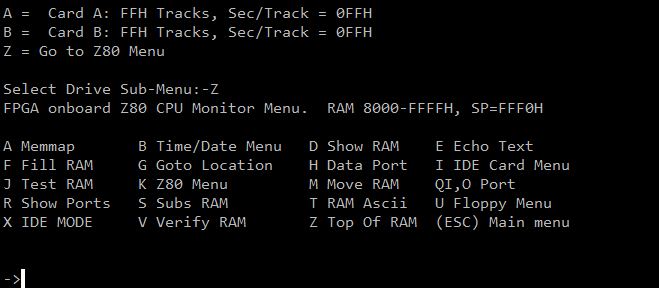
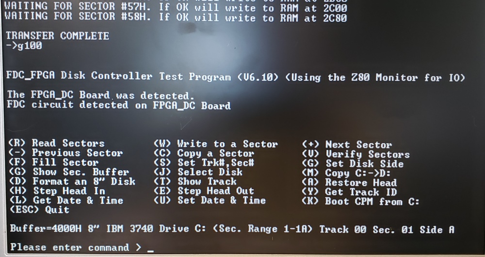
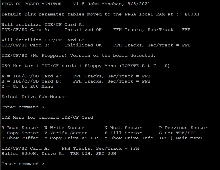
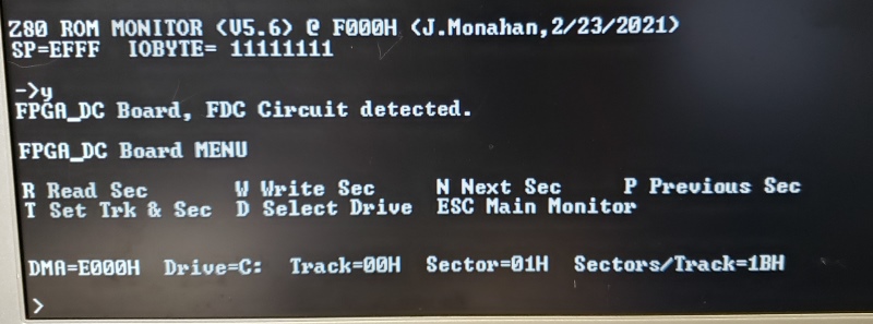
In the Monitor mode, the Z80 can boot up as a typical Z80 "monitor". All external
communications are via an onboard USB port to an external PC software
TTY text window. All the typical Z80 monitor commands you
have seen in the past are there. Here is a picture of the monitor
menu.
Amongst the typical command Z80 menu commands are ones to interface with
the IDE/CF card (and the Floppy disks -- not used with this board).
We will talk about these later, but most are self evident. These
commands simply read/write disk sectors to the onboard RAM on the board
itself. Any S100 bus CPU is completely unaware of this process.
While its critical to the board build/debug process, for an S100 bus
CPU/operating system it is not utilized.
The Disk Controller Mode
of action is the one we normally use when the board is
built. It completely bypasses the above monitor and simply looks at
two I/O ports on the S100 bus. From an external point of view that's
all the S100 bus operating system BIOS sees. The FPGA_DC board on power
up and after initialization simply looks at these ports waiting for a
command (byte) sent from the S100 bus CPU. It
then kicks into action doing whatever 8 bit command the S100 bus sends it.
This is the communication gate between the two systems. It has
to be simple and fast. There is a status port and data port. The
status port bits set/reset automatically depending on the data process.
The complete circuit resides within the FPGA and its Z80 module. The
S100 bus provides the sINP, sOUT, pWR, and pDBIN signals together with the
S100 bus data in/out lines to the FPGA. All S100 bus signals are
switched to the 3.3V levels required by the FPGA with 74LVC245 IC's. The
FPGA Z80 monitor can be configured as we will see below to show in real time the commands being
executed., which drive, track, sector is been utilized etc.
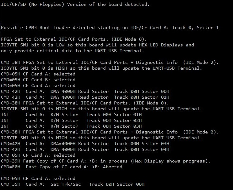
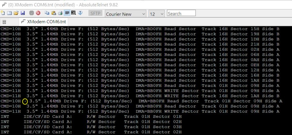
Here is a snap-shot example of the display coming over the USB port:-
This stream of messages will come over a USB port from the board continuously as you boot
and run a disk operating system. This makes BIOS debugging easier. If
bit 0 of the IOBYTE port (SW1) on the board is open the board runs at full
speed but no "breadcrumbs" trail is sent.
The
FPGA_DC.bdf contains the FPGA "schematic" for this and all the
modules within the FPGA. Its fairly complex and should be studied
carefully to understand how this board works. That said, everything
within the FPGA can be treated as a "Black Box" in terms of getting the
board to operate as a disk controller board. You should not have to modify
any of the circuits for normal use.
Within this Disk Controller Mode there are 3 sub-modes in
which the IDE/CF card part of the board can work.
IDE Mode 0.
In this mode the IDE circuit acts identically to the original dual IDE/CF
board mentioned above. The 8255 appears on the S100 bus exactly as for that board.
All software (e.g.. a CPM BIOS), works unchanged. You should be able to
boot any operating system on your old CF cards directly in this mode. This
comes at a price. There is limited diagnostic real time information
passed back on the USB port terminal. The external 8255 port writes do
trigger an interrupt in the FPGA Z80 so it displays the current drive, track
and sector being accessed -- but no more than that.
IDE Mode 1. In this
mode the IDE/8255 circuit is brought under the direct control of the FPGA.
This mode will not work with the old CPM3 BIOS software - unmodified. All BIOS functions
are sent to the FPGA with a few simple Byte commands. All CF card
initialization, drive, track, sector requests can be contained in a few very
simple commands. This exact same command structure approach is used
for all the Floppy BIOS requests as well. In IDE Mode 1 a more
extensive run time display of drive access is sent to the USB port terminal.
IDE Mode 2. This mode is a hybrid of modes 0 and 1.
The IDE circuit is again external to the FPGA but more diagnostic
information is passed back to the FPGA. Card initialization and checkout for
example is still done within the FPGA. For this mode any current BIOS
will need to be slightly modified. The changes are relatively quick and
simple however.
In all cases the BIOS routines for all types of disk access is the same.
Its essentially as we have done for the
ZFDC Floppy disk controller board.
Here are a few commands as examples:
CMD$SEL$DRIVE EQU 5H
;(Re)select an already Initilized drive
CMD_SET_TRACK
EQU
7H
;This will set head request to a specified track
CMD_SET_SECTOR
EQU
9H
;This will set sector request to a specified sector
CMD_READ_SECTOR
EQU
10H
;Read data from the CURRENT sector.
CMD_WRITE_SECTOR
EQU
11H
;Write data to the CURRENT sector.
The important concept to remember with this board is the
same commands are used for
all drives/cards (IDE,
mini SD, micro SD) and as we shall see later for the FDC version of the
board 8", 5" and 3.5" drives). The operating system BIOS
does not have to know anything about the drive initialization, track/sector
seeks etc. As you might expect the is a slight overhead involved
for disk access with this approach. Since the FPGA_DC Z80 is running
at 40MHz for floppy access the bottleneck is always the disk drive -- even
for high capacity double density disks. For the IDE/CF/SD drives/cards
there is a slight delay -- about 2X for sector R/W's. This is unnoticeable
when running CPM3 but does show up in for example a "pure" disk copy of one
card to another. This is why we have IDE Mode 2. In this mode
the actual core sector R/W routines reside in the (CPM) BIOS.
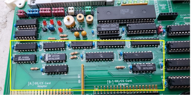
The IDE/CF Card Interface.
For compatibility with the original IDE/CF Card this board also contains a
two IDE interfaces. I brought across
the exact 8255A circuit utilized on our
IDE board. At first this might
seem unnecessary. Certainly an 8255 circuit can be formulated within the
FPGA. However when you total up all the external FPGA pins require for
the 8255 "emulator" and the fact they have to shifted to 5V levels and
they have to be bidirectional ports (all 3 of them), the board real estate is
best served with a single good old fashioned 8255A. Also this makes the
FPGA Z80 code very easy since the code used in all our prior Z80 monitors
can be spliced in directly.
Both the SD and CF cards have way more capacity than CPM can be configured
for and possibly for MSDOS in some cases as well, so in most case we will
utilize only the early sectors on the "drives".
Here is the circuit for the 8255A based IDE/CF card interface on the board:-
In this day and age you are probably not going to use a real IDE hard drive with
a cable (but you can). Instead the drive is built to accommodate an IDE to CF card
adaptors so an actual CF cards can be used.
They typically cost about $6-$10. I have been using the "SYBA Multimedia IDE to CF
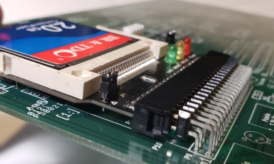
Adapters". We will plug the above adaptor into a right angled 20X2 row of 0.1" pins and
that into a 20X2 female connectors in P1/P9
and P15/P9 (see below).
Since the original IDE/CF Card board came out (in 2004)
SYBA Multimedia has come out with a smaller version of the adaptor. It
behaves exactly the same BUT the IDE connector orientation has been flipped
around. As you look at the front of the adaptor pin 1 is at the back top row
on the right (#2 below). This adaptor needs to be plugged into
P1 and
P9. The older
adaptors plug into
P10 and
P15. Be sure you
add the adaptor to the correct socket. If you use the "old" adaptor
(#1 below), its best not to add the socket for the new adaptor to positions
P1 and
P9.
To utilize SD cards in early designs of this board I utilized SPI SD card
adaptors such as the
Adfruit or
Sparkfun Adaptors. While they worked
fine, actual card access was 10X slower that for CF Cards.
This is due to the single bit SPI public domain interface rather than
the 4 bit licensed interface. Fortunately again there
are IDE to SD card adaptors that completely take care of the complex process
of SD card initialization and access at CF card speeds. Here is a
picture of the one I currently use.
There are also mini to micro SD card adaptors that fit into these units.
So our IDE sockets can accommodate either:-
A Ribbon cable connected "real" IDE hard disk.
A CF Card
A Mini SD Card
or a Micro SD Card.
As far as the software is concerned (see below) all behave the same.
Board Height.
While on adaptors and sockets, there is one major decision you have to make,
and that is the spacing distance between this board and the next board in
the S100 bus. You can either add a 20X2 female socket and a
"standard" 20X2 right angled dual row header to connect it to the adaptor.
This raises the adaptor above the board so that the HEX LED display chips
can be placed in IC sockets, (see picture below). Alternatively
you can use a special 20X2 right angled dual row header to connect it to
the adaptor directly. This is a tight fit. You must use the longer
pins for the IDE adaptor, the shorter pins just make it to the back side of
the board. In this case the HEX LED display chips should be soldered
directly to the board (see picture below). A better socket is the (DigiKey #
S2141E-20-ND) socket which has longer pins. . This makes for a nicer low profile
board with plenty of space before the board in front of it.
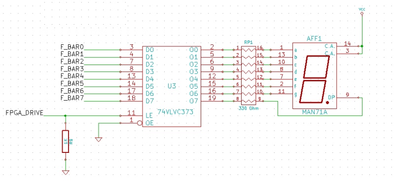
The Drive, Track, Sector LED HEX Display
Interface.
While clearly not essential for the board to function, it's nice to
always have a runtime display of the actual drive/track/sector the BIOS is
working on. In the past we used five TIL 311A LED HEX display on our
IDE and
ZFDC boards. These are
wonderful HEX display LEDs. They convert 4 bits directly into the characters
0,1,2...E,F. Unfortunately they are no longer manufactured by HP and
are in short supply and are thus expensive. The also tend to burn out and
are
power hungry. All modern day 7 segment displays only
decode the digits 0-9 from a 4 bit nibble. In order to "hammer them
into shape" you need to address the 7 segments directly starting with the 16
possible 4 bit nibble values. Trivial to do in our FPGA Z80, but you
also need to latch the outputs for each digit (using a 74LVC373) and drop the
current with an inline resistor network. The 74LVC373 also up's the voltage to
5V. Here is the circuit for one digit.
A very straightforward circuit but unfortunately requiring some 15 IC's for
all 5 Hex LED displays. I could
have used some SMT chips but I know some or our users have difficulty
soldering these. This circuit uses most of the space
on the right hand side of the board. You will see that all 5 digits are
latched in place with separate digit lines from the FPGA. They are not
continuously sequentially scanned in -- saving a major drain on the Z80 overhead. This
gives a nice very steady display.
Notes on CHS and LBA Addressing
On a PC
(at least the early ones), sectors are defined is terms of Cylinders,
Heads & Sectors (CHS format). Parameters in early MS-DOS versions were passed via
software interrupt INT 13H for sector reads and writes. INT 13H
designates sectors in a somewhat convoluted way (for historical reasons),
parameters passed are always as follows:-
AH = 02h
AL = number of sectors to read/written (must be nonzero)
CH = low eight bits of cylinder number
CL = sector number 1-63 (bits 0-5)
high two bits of cylinder (bits 6-7, hard disk only)
DH = head number
DL = drive number (bit 7 set for hard disk)
ES:BX -> data buffer
Because only 16 heads are allowed with this format, a
hard disk can only get to 512MG in size. This is not a problem
for 8 bit CPM systems since disk capacity was always less than 10 MG. To go
to higher disk capacities with later version of MSDOS, the PC BIOS's
utilized the so called "LBA" sector addressing mode. In this
case sectors are numbered on the disk as just one long number. Starting at 0
and working upwards. There are no tracks or heads. We used this format on our IDE/CF
Card board and will use it here as well.
CF cards can be accessed in both CHS and LBA modes. Our FPGA code assumes
all access to the CF card is in LBA mode, starting at sector 0,1,2,3...
SD cards don't even have the CHS mode option. All sectors are accessed
0,1,2,3...
However for CPM (and MSDOS) BIOS software we will work with drives, tracks
and sectors. We will allow for 2 drives of 0FFH tracks and 0FFH
sectors. All sectors will be 512 bytes in size.
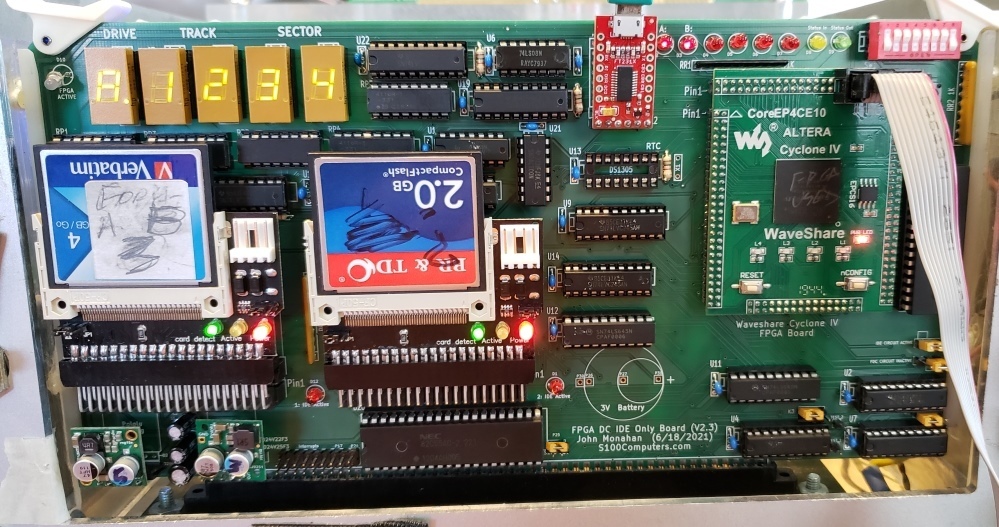
For ease in debugging etc. the 5 digit HEX LED display will display the
current drive, track, sector being accessed in this format. The
operating system never has to know about the CHS to LBA translation taking
place within the FPGA.
Here is a typical display:-
| |
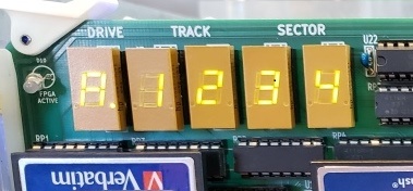 |
This would be the IDE CF card A: with the current sector being Track 12
sector 34.
Step By Step Building the
FPGA DC + IDE Board
The build instructions are fairly simple for this board but because it is a complex board building it should not be rushed. As always, first examine the bare board carefully for scratches or damaged traces, use a magnifying glass if need be. A broken trace is almost impossible to detect by eye on a completed board.
Solder in all the required IC sockets,
resistors, resistor arrays, capacitors, jumpers, and the Pololu 5V and 3.3V voltage regulators. Please be sure you put the
resistor arrays in with the correct orientation of pin 1, (the square pad). An incorrect
orientation is one of the most difficult things to detect/debug on a board
if not noticed. Check their values
before soldering (they are difficult to remove). Insert all jumper arrays.
There appears to be a few variations of
the 74LVC245 20 pin DIP level Shifters chips with "A", "AN" etc. after the
245. As best I can tell so long as they are 20 pin DIPs they are
all OK. I use either Mouser chips # 595-SN74LVC245AN.
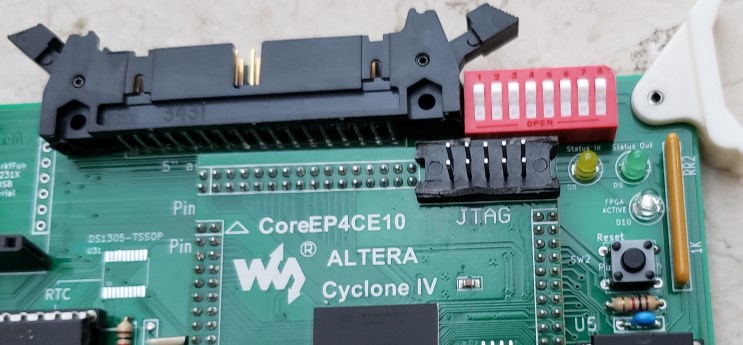
The WaveShare Cyclone IV adaptor can be obtained directly from
Waveshare
or
Amazon
The WaveShare unit uses unusual 2mm dual row female pin connectors. Unlike
to normal 0.1" connectors these are quite rare an expensive (Digi-Key
#S5750-30-ND). You need to carefully cut them to size, carefully cutting off
the extra pins with a wire cutter. Better sockets are available from Mouser
(Preci-dip 833-87-038-10-001101) as part 437-8338703810001101 for
$3.04 each.
Please note the Digi-Key #S5750-30-ND sockets
for the WaveShare adaptor are quite tricky to fit on to the board. I
found the best way to do it is (after trimming to size), push them half way
on to the adaptor pins and then wiggle them to fit the whole unit on to the
S100 board. Figure on spending 10 minutes on this step!
Do not solder them to the board first and then try and press the adaptor
down on them. They are very fragile and internally the leaves will
bend if socket angles are not exactly correct. When in place, check
each pin is visible on the back of the board before soldering. Only
then solder all around. Add as little solder to each pin as possible -
the narrow pins have a tendency to wick up solder internally. The
Mouser ones don't have this problem but you need two of then for the
FPGA side pins. All sockets need to be trimmed to the requires pin number.
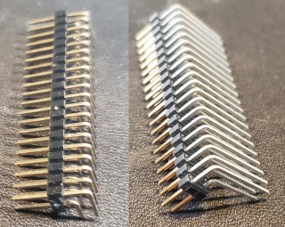
The 2mm spaced male pin headers are DigiKey #0877584416.
One final point here, you will see that many traces go between the FPGA
socket pins on the front of the board. I always worry that the socket pins
during soldering would melt the varnish and contact one of these traces. So
I always insert the sockets just enough to see the pins on the back side of
the board. In other words the socket is slightly above the board.
Try for at least a papers thickness of separation at least between the
socket and the front side of the board.
BTW, to remove the FPGA adaptor, leaver each
corner up a little going round and round. The first time its quite difficult
to get the adaptor out. It gets easier with time.
I use the Adafruit USB serial Adaptor,
but the equivalent SparkFun unit also works fine.
Note there are two sockets for the Pololu 5V and 3.3V regulators. While the older ones
(D24V25F5
and
D24V25F3) are still available
and use P3 and P4, it seems Pololu is suggesting users use the newer
D24V22F5's
(5V, 2.5 Amp) units, it has a different pinout, use this one in P2
(not P3). More recently
they also added the equivalent
D24V22F3
3.3V regulators. Unfortunately in their wisdom they again changed the pinout
connections. You
must use the Pololu
D24V25F3
3.3 V regulator in P4 or the D24V22F3 regulator in
P21. Be sure you get these regulators/ correct. To be safe once inserted, check
the voltage in your system on a 5V and 3.3V IC, (see the schematic) with no
chips yet inserted on the board. 5V and 3.3V going to the correct pins of the FPGA
adaptor. (5V going to the 3.3V pins will blow the unit!). Please
note Pololu has come out with more 5V and 3.3v regulators. Please
examine the pinouts and match them with the board sockets.
Unfortunately the newer 5V and 3.3V units look exactly the same on the
surface. Presumably some of the internal resistors are different to give 5V
and 3.3V.
Note recently the above Pololu regulators have gotten hard to find and have
become expensive. Pololu now has more options to pick from.
Examine the pinout of any of their 5V or 3.3V regulators and place
them in one of the two sets of slots above.
When adding the LED's be sure to orient them correctly. (Usually the longer
lead in the square pad).
The 20 pin DIP version of the
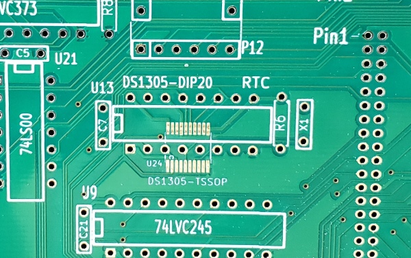
Maxim RTC chip is
currently in short supply. In case people cannot obtain one I have
added a footprint for the SMD version of the chip as well. They
both work exactly the same. Be sure not to add the U13 DIP socket if you
intend to use the SMD chip.
There are many types/sizes of 3V coin batteries and adapters. Jameco sells
many holders. The 1" #236996 with a CR2032 is common. So long as it's 3V
types don't matter. The RTC chip battery should last for years!
Please take care to not "slobber" solder on the sockets. They are very
closely spaced on this board with vias often close to a socket pin -
particularly for the FPGA adaptor sockets.
At this point insert the board into your system and check your S100 bus Z80 monitor
boots fine. If not check for solder bridges etc. Also do one last
check to be sure every IC solder pin is soldered. Seems trivial, but I
don't know how many times I got caught with this error.
Next we need to solder in the three ICs U10, U15 & U16
directly to the board. If
possible use known working 74LVC245's from a previous board. You don't
want to have to remove a faulty one later. Take care not to scorch the
chips. If possible have the chip pin just barely show on the back of the
board for soldering.
Here is a picture of (a
prototype version) the board at this stage:-
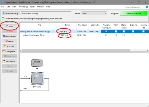
If you are not completely familiar with programming the Cyclone IV FPGA
please study in detail this write-up
Programming a Cyclone IV FPGA.
Carefully insert the WaveShare
Cyclone IV adaptor in its sockets. Power on the computer.
"Virgin" Cyclone IV Adaptor boards from WaveShare may have a FPGA
preloaded with a program (in the
EPCS16 Flash RAM) that already that pulses its
4 onboard LEDs. Previously programmed by you FPGA boards of course will
not.
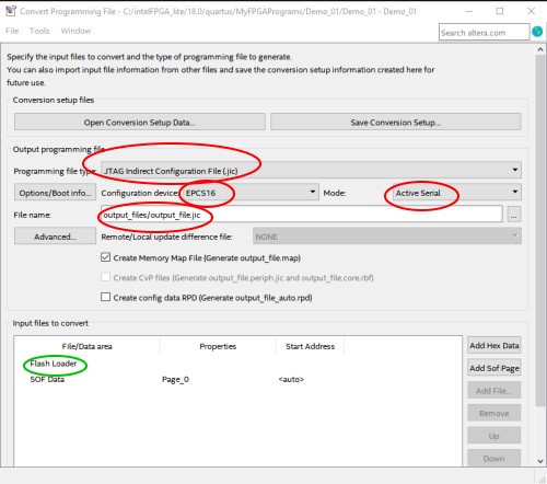
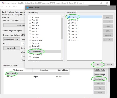
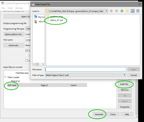
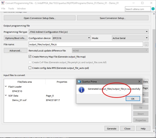
In any event open the Quartus FPGA_DC project folder (the expanded
FPGA_DC.ZIP download, see bottom of this
page) and program the FPGA using the
FPGA_DC.bdf
file.
Now would be a good time also to study in detail the
FPGA_DC.bdf file to
understand how the board "works". Remember the FPGA utilized its own
internal 30-40 MHz Z80 and so utilizes a .HEX file for its ROM code. This
.HEX file resides in the FPGA_DC\ROM_HEX_FILES sub-folder. The source for
this file is FPGA_DC.Z80. You don't need to alter this file for
normal use but its also provide in case you need to.
Should you wish to "play around" with this file, I supply it and its
components in the folder
FPGA_Disk_Controller Board where
it can be assembled on a
PC using Altair.com etc.
Be sure to move the final FPGA_DC.HEX
file to the Quartus FPGA_DC\ROM HEX FILES
folder when done as Quartus is counting on finding the
FPGA_DC.HEX file there (or readjust the ROM Module Properties in
the .bdf file)
If you program the onboard Cyclone IV FPGA at this point nothing will happen
except the LED D10
(Board Active) LED will pulse. This must happen. Do not go further
unless it does.
Next install the following IC's:-
U2, U4, U7, and the RAM chip U5.
To activate the IDE/CF Card circuit within the FPGA jumper K4 1-2 and K2
2-3.
IEEE-696 16 bit S100 bus port IO addressing is assumed (the upper 8 lines
being zero) for this board. This can be easily bypassed within the FPGA
(Jumper K1 1-2). Do so if your CPU board does not zero the high
address lines for port I/O. To be safe we will jumper K1 1-2 for now. Note
16 bit CPU's will probably require K1 2-3.
Install the Sparkfun
FT231x USB adaptor. Note it has a jumper on its back for 3.3V operation,
use 3.3v not 5V. You can
solder the adaptor directly to the board or use sockets. See the
section above on soldering sockets. I suggest direct
soldering. Note the USB FT231x
adaptor actually has 3 sockets. The two side ones are not used here and are
only there to steady the adaptor on the board. I use only pin 1 in each
case. You can also use the
Adafruit CP2104 USB adaptor equivalent adaptor. Perhaps it's just me, but sometimes
I've
had problems getting this adaptor to link up with my PC's.
The default software on this board assumes a USB port running at 38,500 BAUD, 2 stop bits, no parity.
(This can be changed within the FPGA_DC.bdf file). There are a number
of Windows/PC programs you can use to receive and display the data. I
like
Absolute Telnet
from Celestial Software, but others are free.
The board has an "IOBYTE" switch (SW1),
which defines what the FPGA_DC Z80 monitor
does on power up. The default mode, all switches open, (no switch) causes
the Z80 monitor to get
0FFH
from port
46H after a reset. This is the boards normal mode of
operation but we will not use it yet. Currently only two
switches are utilized:-
Bit 0 (Pos
8), (Reading left to right), when closed, (xxxxxxx0H),
this causes the board to send status information to the USB port during
every step of its operation. A remote PC can thus watch how commands sent
from the S100 bus are operating during "disk" operations. This slows down
the Operating System BIOS a little but is invaluable for debugging etc. When
open no commands are sent.
Bit 7, (Pos1),
when closed, (0xxxxxxxH),
this causes the board upon reset to bypass the S100 interface and go
directly to its onboard monitor. The onboard monitor contains all the
"normal" commands for a Z80 CPU, display/change RAM, ports etc. but it also
contains two very special command I
and
U.
Place the board in the S100 bus with
SW1 positions
8
and
1
closed. Power up and again load the
FPGA_DC.BDF
file into the FPGA. Upon reset the FPGA will boot up its Z80 monitor. You
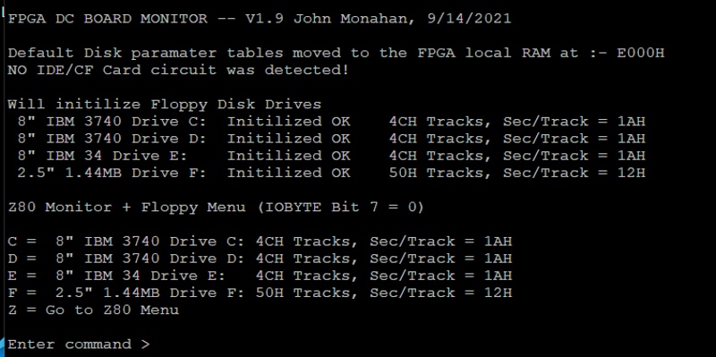
should see the following display:-
For now just use the Z command. This will bring you directly to the
FPGA Z80 CPU monitor. You should see the following:-
Most of these commands should be familiar to our users. (The
X command BTW,
is not yet implemented).
Play around with the regular Z80 monitor commands (except
I,
U and
X)) at this stage to get
comfortable with the interface.
For example the A command will show
you the "Memory Map" for the Z80 on the board.
Next we will install the IDE/CF card circuit.
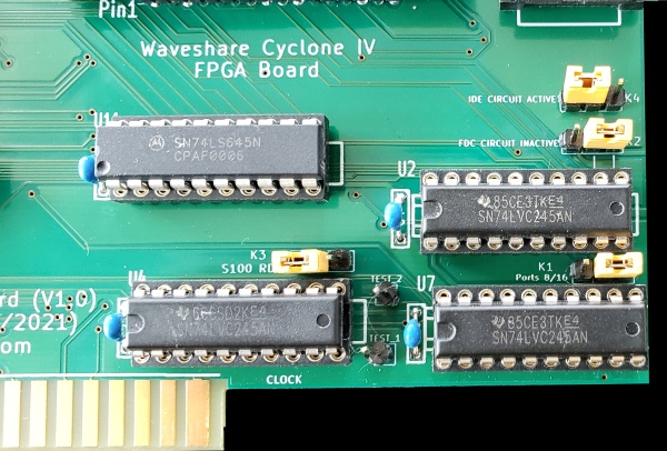
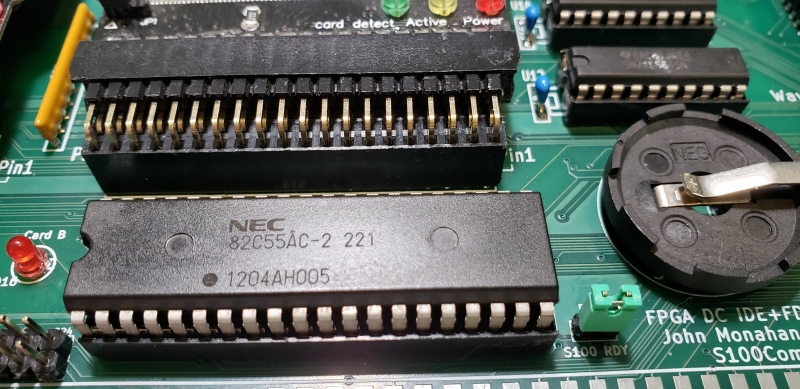
Install the 82C55, U26 chip.
Add U26 (I have had a number of CF card initialization problems with some
82C55A's e.g. NEC and OKI chips. The only reliable chip I find is the
NEC 82C55AC-2).
Use this (common) chip.
Add U9 and U12 and U11 and U14. Note U12 & U11 are regular 74LS245s (or better 74LS645s).
Add U1, U6, U20 and U21.
Jumper K1 2-3, K3 1-2 and P25.
Install one or both of your IDE adaptors each with CF cards.
Power up, load up the FPGA again and from the USB port menu select the "A"
menu option.
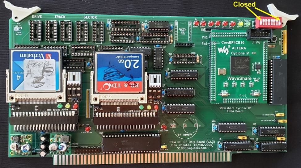
The board should look like this at this stage:-
The IDE Sub-menu should come up as shown here:
What remains is the circuit to display the current Drive, Track and Sector in
the LED Hex Displays.
Before adding the chips please re-read the section above about "Board
Height". Add a the chips with or without sockets (see above).
Be careful with the MN71A HEX displays -- the
pins are a little fragile.
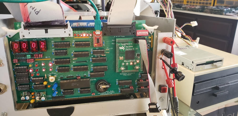
Here is a picture of (a prototype version) of the board at this stage.
Finally you can add RTC Chip and 32.768 KHz Oscillator and coin battery
holder. One or two sizes can be used, but be sure to have the + terminal on
the RHS.
You can bring up the RTC menu from the main monitor, "Z" command, then "R".
The menu is fairly clear, but one unusual thing about this chip is you must
"Activate" it ("A" menu option) to start the clock the first time (even if
you set the time etc.)
Here is the RTC menu:
The board is now fully setup. What remains to be done is understand the
fairly extensive software menus and commands.
THE FPGA Z80 MONITOR COMMANDS
As described above the board can initialize in three completely different ways.
If Bit 7
& 0, (Pos1+8),
is closed, the Z80 reads (0xxxxxx0H) from
the IOBYTE port (46H)
and goes into its internal monitor mode. There is in fact no
connection
with the S100 bus. The only communication with the outside world is via
the USB port.
Normally one would not go to the
Z command but
would select one of the two "Drives" A or B.
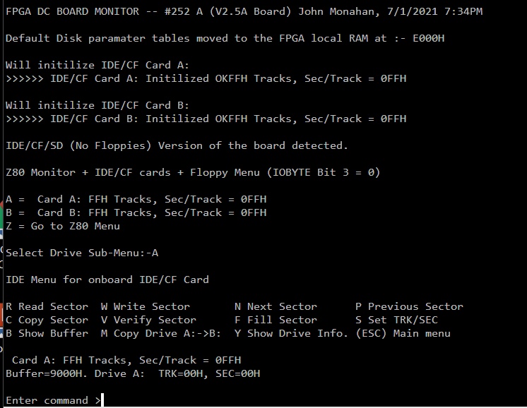
Here is the sub menu for the IDE drive:-
The "current sector" under consideration is always shown. In this case
Drive 1: Track 0, Sector 0.
If we enter "R" we will display its contents (all 512 bytes):-
Most of the commands are self explanatory. The copy command copies the
current sector to another specified sector location on the same disk. The
verify command checks they are identical.
The
"Y" command
displays information about the "disk".
A few non-obvious shortcuts:-
If asked for a sector number, a CR will enter the current Track and , Sector.
All track, sector information are in hex values in the format xx,xx (+CR).
So a maximum of FFH,FFH tracks and sectors on a drive.
So a "R" command above followed by a CR will display the sector on Track 0,
Sector 0
The "R" with 12,34 then a CR will display the sector on Track 12, sector 34.
While we will see later when we operate from the S100 bus, in this "local"
mode you cannot move/view etc. sectors across drives.
To explore a different drive enter ESC and select from the menu another
drive.
THE S100 BUS INTERFACE
WITH THE FPGA_DC + IDE CIRCUIT
Having satisfied ourselves that we have the onboard hardware working
correctly we will now proceed to have the board interface with the S100 bus
as a true disk controller board.
That said, do not go to the S100 bus mode unless all the above commands work
flawlessly.
First we open
Bit 7, (Pos 1) of SW1. This dramatically
changes how the FPGA Z80 operates after reset. The FPGA_DC
IDE board now comes up
in normal work mode. Initially its Z80 scans the S100 input port waiting to
receive a "Handshake CMD".
This is a
21H byte sent out on
the S100 bus to output port (81H).
It responds by echoing this byte back on
the S100 bus input port 81H.
With this the S100 bus Disk Operating system BIOS knows the FPGA_DC board is
alive and well. The two then continuously interact with other via
series of single byte commands. Normally this is done in your
operating system BIOS.
This CMD driven approach was first used with our
ZFDC Floppy disk controller board now
some 10 years ago! It turned out to be very successful and reliable
allowing a very simple CPM BIOS to access 8", 5" and 3.5" floppies is over
50 different formats with a few very simple set of byte commands. I used
the same idea we have here, the boards local Z80 does all the dirty work of
finding a sector on a requested drive given just the track and sector
number. In order to simplify the BIOS
software with all 3 boards in this series of FPGA_DC boards will use the same CMD format.
We will just add a few extra commands not found on the original ZFDC board
commands.
Here are the main commands for this FPGA_DC board:-
CMD$SEL$DRIVE
EQU 5H ;**** (Re)select an already initialized drive
CMD$SET$SIDE
EQU 8H ;**** This will set the active side for a
floppy disk
CMD$SET$TRK$SEC
EQU 35H ;Set new current TRACK+SECTOR on current drive
(new)
CMD$READ$SECTOR
EQU 10H ;**** Read data from the CURRENT sector (on
current track, drive).
CMD$WRITE$SECTOR EQU
11H ;**** Write data to the CURRENT sector (on current
track, drive).
CMD$HANDSHAKE
EQU 21H ;**** Handshake command only sent during board
initialization/testing
CMD$SET$IDE$MODE EQU
38H ;Set IDE drive hardware mode on FPG_DC Board (Internal
or External)
; Second Byte 0 = External IDE mode + Interrupt
driven info (Default Mode).
; Second Byte 1 = External IDE mode + CMD driven
info
; Second Byte 2 = Local FPGA Board IDE mode + CMD
driven info
CMD$FAST$COPY$AB EQU
39H ;Special CMD to fast copy CF Card A:->B: (All within
FPGA_DC Board software)
CMD$SET$HOME
EQU 0AH ;This will set floppy disk head request to Track 0
of CURRENT floppy drive
CMD$GET$TRACK$ID EQU
0FH ;Read the CURRENT FLOPPY TRACK ID
CMD$STEP$IN
EQU 0BH ;Step head in one track of CURRENT floppy drive
CMD$STEP$OUT
EQU 0CH ;Step head out one track of CURRENT floppy drive
CMD$SEEK$NV
EQU 0DH ;Seek to track with NO verify of CURRENT floppy
drive
CMD$SEEK$TRACK
EQU 0EH ;Seek to track to (IY+DRIVE_TRACK) with the track
verify bit set on CURRENT drive/format
CMD$TRACK$DUMP
EQU 15H ;Dump complete CURRENT floppy track to S-100
system
INFO$READ$SECTOR EQU
42H ;Send info, read sector (Actual Sec Read done
externally)
INFO$WRITE$SECTOR EQU 43H
;Send info, write sector
CMD$FORMAT$DISK
EQU 44H ;Format the disk in the of the CURRENT drive
CMD$FDC$COPY
EQU 45H ;Fast Copy Disk C:->D:
CMD$GET$TIME
EQU 80H ;Get Time and Data from FPGA DC Board RTC
CMD$SET$TIME
EQU 81H ;Set Time and Data on FPGA DC Board RTC
CMD$BOARD$CONFIG EQU
82H ;Get FPGA_DC Board hardware configuration
; Bits 7&6 contain IDE & FDC circuit flags
; Bits 1&0 contain IDE Mode (0,1,2)
For a CPM (or MSDOS) BIOS only the 7 commands in yellow are needed. The rest
are extra for testing and diagnostic purposes.
That said the commands absolutely have to be bullet proof and 100% reliable.
The S100 bus OS BIOS does not know or care what type of disk is talking to.
It also has to be fast. There is a single 8 bit port bridge between the two
systems and a second status 2 bit port. The core of
FPGA_DC.BDR
circuit is shown here:-
While it is not necessary to understand this circuit to use the board you
might want to study it to get a feel how the board works. In essence
the FPGA Z80 just sits waiting for its port
80H (bit 0)
to get a CMD
byte (21H)
from the S100 bus. It reads the byte
automatically sending back to the S100 bus
port
80H
an acknowledge byte (21H)
that the data has
been read. The FPGA Z80 then processes further commands each time sending
a "CMD Complete" byte indicating the work is done.
Commands may have follow on bytes of data. For IDE/CF Card sector reads and writes for
example there
will be 512 of these. The S100 bus status ports (bits 0 & 7) on
both sides is port
81H.
While this sounds complicated in actual reality writing BIOS software is
very simple.
Further for debugging, as I mentioned above if we open
Bit 0, (Pos 8) of SW1 each and every command processed by the FPGA
Z80 will first be listed on the USB TTY output.
Here is a "breadcrumbs" trail of where we (start) copying CF card in drive
A: to B:
This brings us to the next part of the software -- the S100 Bus diagnostic
program.
The FPGA_DC+IDE Diagnostic Program
Before we take on the fairly complicate task of writing a full blown CPM3
BIOS to utilize this unique board it would be quite useful to have a S100
bus diagnostic program that sits in RAM at 100H upwards to test the board
interface. We essentially transplant the FPGA Z80 monitor disk
commands to the S100 bus. As we will see we elaborate on them to allow
multi disk transfers, reliability checks and anything else that assures us
the board can handle a CPM3 or MSDOS BIOS.
For debugging etc. I have written a Z80 program (IDE_DIAG.Z80)
that resides in the S100 bus RAM at 100H. It assumes the FPGA_DC ports
are 80H and
81H and the Console
IO is our
Propeller Console IO board (ports
0H
and
1H). Because it
resides at
100H it can be loaded
with CPM (later!), but for now you must download it from your PC via
a serial link and the Z80 Master monitor X command (X100).
By now this process should be familiar to most of our users. There are
other ways to do this, but in the end you need to have the
IDE_DIAG.COM (or
IDE_DIAG.HEX)
reside at 100H in RAM and jump to
100H from a Z80 S100
bus monitor.
First we open
Bit 7, (Pos 1) of SW1. This dramatically
changes how the FPGA Z80 operates after reset. The FPGA_DC
FDC board now comes up
in normal work mode. Initially its Z80 scans the S100 input port waiting to
receive a "Handshake CMD".
This is a
21H byte sent out on
the S100 bus to output port (81H).
It responds by echoing this byte back on
the S100 bus input port 21H.
With this the S100 bus Disk Operating system BIOS knows the FPGA_DC board is
alive and well. The two then continuously interact with other via
series of single byte commands. Normally this is done in your
operating system BIOS.
It will sign on as follows:-
After you select the drive you wish to work with the above menu will
appear.
As you can see this is a more elaborate version of the onboard FPGA monitor
commands.
Again most of these commands are self-evident. A number take one or more
follow-on single byte parameters. Some return to the S100 bus one or
more single byte values. In all cases they must return the
CMD_COMPLETE (F0H)
byte value confirming to the S100 bus BIOS that the requested operation
completed successfully. Anything else is regarded as an error and the BIOS
must act accordingly.
On the FPGA_DC Z80
monitor side the interpretation of these commands can be quite involved but
on the S100 bus side (all the user has to be concerned with in writing a
BIOS) it makes things very simple. In fact almost all the commands are one
of five commands:-
CMD_SEL_DRIVE EQU
5H ;**** (Re)select an already Initilized
drive
CMD_SET_TRACK EQU
7H ;**** This will set head request to a
specified track (ONLY)
CMD_SET_SECTOR EQU 9H
;**** This will set sector request to a specified sector (ONLY)
CMD_READ_SECTOR EQU 10H
;**** Read data from the CURRENT sector (on current track,(side),drive).
CMD_WRITE_SECTOR EQU 11H
;**** Write data to the CURRENT sector (on current track,(side),drive).
CMD_INIT_DRIVE
EQU 30H ;Select AND Initilized the current drive
All drives are always available. The default drive format for our IDE board is up to 0FFH
tracks, 0FFH sectors/track and 512 byte sectors.
These parameters can be
easily changed by a "Disk Parameter Table" at the end of the FPGA Z80
monitor code (or by setting bits 1 & 2
of the IOBYTE
switch, see below).
For those that have built and used the
ZFDC floppy disk controller board they will recognize this command
driven approach. However because CF and SD cards are quite
different the actual commands and the Disk Parameter Tables are different. The
FPGA Z80 IX register always points to the start of this table.
Here is the Disk Parameter table for an CF Card Drive:-
IDE_DRIVE_1:
DB CFCARD ;0H, (0FFH), DISK_TYPE (Default IDE Card/Drive)
DB 0FFH ;1H, Default Card Present
DB IDE_CS_1 ;2H, DRIVE_CS, actual Drive CS* Line
; Bits 0,1 are used for drive hardware selection (00=A, 01=B,10=C,11=D)
; Bit 2, 1 if side A is selected, 0 if Side B
; Bit 3, 0 if 8" disk, 1 = 5" disk
; Bit 4, 0 if Single Density, 1 = Double Density
; Bit 5 WD2793 INTRQ 1=ON, 0=OFF
; Bit 6 Write protect flag 0 = ON, 1 = OFF
; Bit 7 Drive Head load (currently unused)
DB 1 ;3H, Drive NUMBER
DB 0 ;4H, INITILIZED, uninitialized
DB 2 ;5H, 512 Bytes/sec flag
DB 0 ;6H, Tracks set aside for operating system (e.g. CPM 2 for floppies)
DB 0AH ;7H, HEX of Drive letter
DB 'A' ;8H, ACCII Character for Drive
DB 0 ;9H, First sector #
DW 512 ;0AH, <------ 512 Bytes/sec
DW 00FFH ;0CH, SECTORS PER TRACK:- (Was 3CH (60)for my on old CPM3 for Kingston CF 8G). (Note. No +1 for cards)
DW 00FFH ;0EH, Max Tracks
DW 0000H ;10H, TRK, Current Track
DW 0000H ;12H, SEC, Current Sector
DB 0H ;14H, Side
DB 0 ;15H, Formatting (Not used for SD/CF cards)
DB 0 ;16H, GAP1 ""
DB 0 ;17H, GAP2 ""
DB 0 ;18H, GAP3 ""
DB 0 ;19H, GAP4 ""
DB 0 ;1AH, GAP4R ""
DB 0 ;1BH, GAP fill byte
DB 0E5H ;1CH, CPM Sector data fill byte
DB 0 ;1DH, Special Flag
DB 0000H ;1EH, Skew Table (Not used for SD/CF cards)
DB 0 ;20H, Format Number
DW 0000H ;21H, Track Size
DB 0 ;23H, Number of (Floppy) disk sides (Not used for SD/CF cards)
DB ' IDE/CF/SD Card A: ',0 ;24H
So the value of Bytes/Sector would be
(IX+SEC_SIZE_BYTES), where
SEC_SIZE_BYTES = 0AH.
The advantage of this command driven approach is that the current S100 bus
CPU does not have to go into DMA mode or sync the bus with wait states when
reading or writing sectors. Any of our S100Computers CPU boards, in
fact in theory, any manufactured CPU board, should work in this system.
The downside is that disk access is a little slower. Not as slow as
you might think however because while the requested sector parameters are
passed back and forth with above commands and handshaking, the actual
512 bytes of data transfer across as a block over the connecting bridge
port one byte immediately after the other using the Z80 block IO
instruction. Normally you will notice no
difference with say a few sectors moved with CPM or even MSDOS.
However a total disk copy from one drive to another will be slower. The
monitor in fact has a special disk copy command to help with this (CMD_DRIVE_COPY
EQU 43H)
a little. Remember these CF and SD cards have an enormous capacity --
way outside early days CPM or MSDOS. Copying the first few "tracks"
usually is all that is required.
For those that wish to play around with the software there is 512K of RAM
available to the Z80 FPGA. Some fancy sector caching routines could be
implemented. Also for MSDOS, multiple sectors could be written
or read with a single command. If you develop code improvements please
let me know.
The Real Time Clock (RTC).
All 3 boards have a DS1305 RTC
chip. This is one example where using a FPGA really shines. With
its 3 wire SPI connection to the FPGA with one chip you get a complete
RTC read and write circuit. Whole S100 boards in the past were
required for this function. The Calendar/Time settings can be set
within the Z80 Monitor or from the above FPGA S100 Bus diagnostic program
(see below). The circuit and software is identical for all three
boards. The chip defaults to 24 hour format. You must have the
coin battery present and you must use the Monitor to initialize the chip for
the very first time (Monitor B, CMDs).
Here is a picture of the interface using the FPGA S100 Bus diagnostic
program:-
The data returned to the S100 Bus with the 81H Command is in the format of
the following 14 character string:-
20210722131004
All ASCII characters. The format is 24 hours.
FPGA_DC + FDC Board.
This board has much in common with the above FPGA_DC+IDE Board.
Instead of an 8255A and two IDE sockets we have a Western Digital 2793
Floppy Disk controller and two ribbon cable connectors along the top of the
board to hook-up floppy disks.
The build instructions are exactly the same as is the software. The
main difference is the replacement of the 8255A with the WD2793 chip.
Study this chips circuitry carefully in the schematic. Critical are the two
0-50K Ohms Pots (RV1 and RV2)
and the 0-50pF Cap C12. Solder these carefully to the board taking care to
place them in their correct orientations for the center tap. We will
adjust them later.
Note the Diode D14 should be at least a IN4005 1Amp diode. It's there
to reduce the voltage going to the HEX displays so they don't run too hot.
As for the IDE board you need to decide if you will use the 20 Pin DIP or
SMD version of the RTC chip (U13).
| |
 |
Solder in all the sockets, jumpers, resistors, caps and the 50 and 34 pin
connectors P9 and P1.
Be sure the Pololu 5V and 3.3V regulators are the
correct types and deliver the
correct voltages to the WaveShare FPGA adaptor before inserting it.
Please note Pololu has come out with more 5V and 3.3v regulators.
Please examine the pinouts and match them with the board sockets.
Unfortunately the newer 5V and 3.3V units look exactly the same on the
surface. Presumably some of the internal resistors are different to give 5V
and 3.3V.
Here is a picture of the (prototype) board at this stage:
| |
 |
Next solder directly to the board the three 74LVC245s U10, U15 and U16.
If possible use known working chips you don't want to remove a faulty one
later.
Carefully insert the WaveShare
Cyclone IV adaptor in its sockets. Power on the computer.
"Virgin" Cyclone IV Adaptor boards from WaveShare may have a FPGA
preloaded with a program (in the
EPCS16 Flash RAM) that already that pulses its
4 onboard LEDs. Previously programmed by you FPGA boards of course will
not.
In any event open the Quartus FPGA_DC project folder (the expanded
FPGA_DC.ZIP download, see bottom of this
page) and program the FPGA using the FPGA_DC.bdf
file.
Now would be a good time also to study in detail the
FPGA_DC.bdf file to
understand how the board "works". Remember the FPGA utilized its own
internal 30-40 MHz Z80 and so utilizes a .HEX file for its ROM code. This
.HEX file resides in the FPGA_DC\ROM_HEX_FILES sub-folder. The source for
this file is FPGA_DC.Z80. You don't need to alter this file for
normal use but its also provide in case you need to.
Should you wish to "play around" with this file, I supply it and its
components in the folder
FPGA_Disk_Controller Board where
it can be assembled on a
PC using Altair.com etc.
Be sure to move the final FPGA_DC.HEX file to the Quartus FPGA_DC\ROM HEX FILES
folder when done as Quartus is counting on finding the
FPGA_DC.HEX file there (or readjust the ROM Module Properties in
the .bdf file)
If you program the onboard Cyclone IV FPGA at this point nothing will happen
except the LED D10
(Board Active) LED will pulse. This must happen. Do not go further
unless it does.
LEDs L1 and L2 on the WaveShare FPGA board will also light up - this is
normal (it depends on how they were programed in the .brd file).
Next install the following IC's:-
U2, U4, U7 and the RAM chip U5. (U10 is already installed).
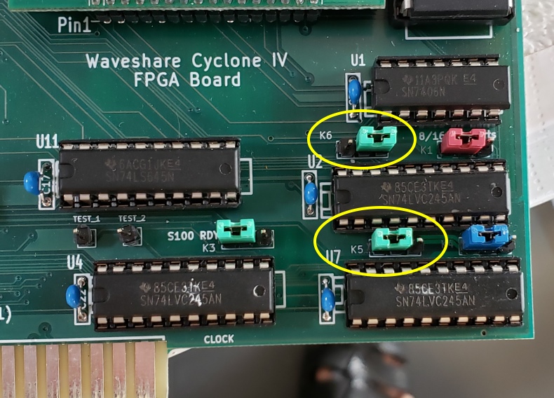
To activate the FDC Card circuit within the FPGA jumper K6 2-3 and K5
1-2. Note it's very important you get these two jumpers
correct.
IEEE-696 16 bit S100 bus port IO addressing is assumed (the upper 8 lines
being zero) for this board. This can be easily bypassed within the FPGA
(Jumper K1 1-2). Do so if your CPU board does not zero the high
address lines for port I/O. To be safe we will jumper K1 1-2 for now.
Note 16 bit CPU's will probably require K1 2-3.
Install the Sparkfun
FT231x USB adaptor. Note the Sparkfun 231x board
(current part number BOB-13263) is designed to be compatible with both 3.3 V
and 5V (TTL) logic circuitry. The “jumper” on the back of the board is only
used to select whether 3.3V or 5V (derived from power supplied by the USB
cable) is provided to the board’s Vout pin.
Since the FPGA floppy controller board does not make use
of this Vout pin – it is a “no connect".
You can
solder the adaptor directly to the board or use sockets. See the
section above on soldering sockets. I suggest direct
soldering. Note the USB FT231x adaptor actually has 3 sockets. The two side ones are not used here and are
only there to steady the adaptor on the board. I use only pin 1 in each
case. You can also use the
Adafruit CP2104 USB adaptor equivalent adaptor.
Note if you use a ribbon cable socket with ejectors (recommended), the
spacing on the LHS of the socket is very close to the USB adaptor.
I filed a little of the plastic from the side of the socket for a
better fit.
The Sparkfun adaptor fits better than the Adafruit adaptor BTW.
The default software on this board assumes a USB port running at 38,400 BAUD, 2 stop bits, no parity.
(This can be changed within the FPGA_DC.bdf file). There are a number
of Windows/PC programs you can use to receive and display the data. I
like
Absolute Telnet
from Celestial Software, but others such as
puTTY and
TeraTerm are free.
The board has an "IOBYTE" switch (SW1),
which defines what the FPGA_DC Z80 monitor
does on power up. The default mode, all switches open, (no switch) causes
the Z80 monitor to get
0FFH
from port
46H after a reset. This is the boards normal mode of
operation but we will not use it yet. Currently only two
switches are utilized:-
Bit 0 (Pos
8), (Reading left to right), when closed, (xxxxxxx0H),
this causes the board to send status information to the USB port during
every step of its operation. A remote PC can thus watch how commands sent
from the S100 bus are operating during "disk" operations. This slows down
the Operating System BIOS a little but is invaluable for debugging etc. When
open no commands are sent.
Bit 7, (Pos1),
when closed, (0xxxxxxxH),
this causes the board upon reset to bypass the S100 interface and go
directly to its onboard monitor. The onboard monitor contains all the
"normal" commands for a Z80 CPU, display/change RAM, ports etc. but it also
contains two very special command I
and
U.
Place the board in the S100 bus with
SW1 positions
8
and
1
closed. Power up and again load the
FPGA_DC.BDF
file into the FPGA. Upon reset the FPGA will boot up its Z80 monitor.
You
should see the following display:-
As for the
FPGA_DC IDE board first utilize the Z command to checkout the
"standard" Z80 commands.
They must work correctly before going
further.
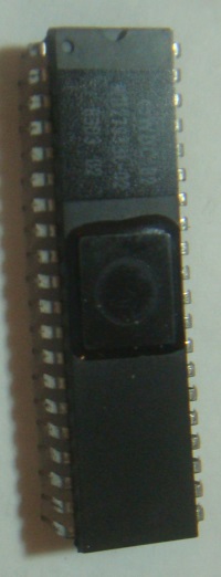
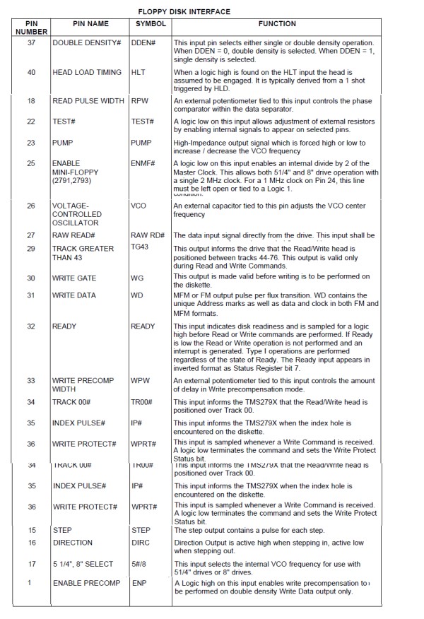
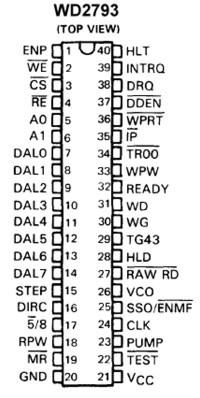
WD2793 Hardware
Like the earlier 1791/1795 chips the
WD2793 consists of a 40 pin chip with many of the same data and control lines as
the earlier 179x
series. In order to fully understand their function you should read the detailed
description of how the WD2793 FDC chip works.
The complete data sheet can be seen
here.
You should read this data sheet in detail to understand much of what I
have below.
Let us first look briefly at the function of the 40 pins:-
Most of the pins are fairly straightforward and should need no further
discussion. Pins #26 and #33 as we shall see, do need to be adjusted, but
Western Digital (by this stage) made it easy to do with a special test pin
(#22). The one complication in any system is if you intend to use the chip
with both 8" and 5" drives mixed together. Because the data rate of a 5"
drive is half that of an 8" drive the clock frequency has to be divided in two.
Pin #25 is set aside for this use.
One very important control pin is INTRQ (#39). This pin pulses high (very
briefly) when every a command is completed. We will gate the output of this pin
going to the NMI pin of the Z80 such that (if desired) the FPGA Z80 will experience a
NMI interrupt whenever the WD2793 completes its current command (seek, read a
sector, format a track etc.). This is a very convenient and efficient way to
synchronize the two chips and make sure the system does not "hang" with for
example a false disk command or data.
WD2793 Software
All Western Digital FDC chips have at
their base port a key "status" port that continuously displays important
information about the chips actions and results. This is reflected in a
series of bit flags. The actual meaning of these bits changes depending on what
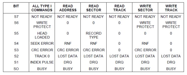
the chip has being doing. Here is a summary of the bit flags for the most
common uses:-
The challenge with any disk controller is matching the data rate of the stream
of data bits coming in from the disk surface with the capability of a CPU's
ability to place the corresponding bytes in memory AND at the same time decide
when the job is done. In the early S-100 days when only 4MHz Z80's were
available, the Z80 simply could not keep up. In other words the Z80 was not
fast enough to continuously monitor the status register status bits AND at the
same time take data from the data port and place it in RAM -- particularly
in double density modes. Two basic ways around this were used. One was to
use a dedicated DMA controller on board (which was fast enough) -- but this
sometimes caused conflicts with other (pre-IEEE 696) S-100 boards. The
other simply took account of the fact that IF there are no errors, one knows
exactly how many bytes to expect (or send) and you can lock the data rate of the
FDC to that of the Z80 utilizing the Z80's block I/O instructions by inserting
CPU wait states during each bytes transfer at the same time counting the
total number of bytes processed.
Fortunately utilizing our 40MHz FPGA Z80 we don't have to use these
round about approaches. The Z80 can simply input individual disk bytes AND
at the same time look at the WD2793 status port to see when the next byte is
available (bit 1, the DRQ bit goes high). That said things are still very
tight. You really have to watch your clock cycles. To input a sector
here is the key code I use:-
READ_SECTOR:
LD
DE,Sector_Size
LD HL,DMA_Address
LD C,Data_Port
CHK_STAT:
IN A,(WD2793_Status)
RRA
RRA
JR NC,CHK_STAT
;Very fast way to check the DRQ status bit
IN A,(C) ;Very
fast way to input data from [C] port
LD (HL),A
DEC DE
LD A,E
OR A,D
JR NZ,CHK_STAT
Using this very efficient code a 40 MHz Z80 is able to keep its head above water!
Interestingly using the special Z80 INI instruction did not work with the
circuit on this board. It's unclear to me why. Even with the above code the
FPGA Z80 clock needs to be 40 MHz. A faster CPU makes no difference
and indeed may be unreliable since you are way outside the specs of the WD2793
chip. Code like this in fact can be utilized to read or deposit a whole
track on a disk.
All of the above is perfectly fine so long as there are no errors. However if
for some reason the WD2793 comes up short in getting bytes from a sector (a
wrong formatted disk was used for example), the system will hang. There is
not enough time to incorporate a software timeout counter in the loop.
What could be done is setup a watchdog timer
in the FPGA such that, IF, a
sector is not read before the timer times out, it triggers a NMI interrupt on
the Z80 which then causes the Z80 to brake out of the above loop and act
accordingly. If the sector is read/written properly in time it turns off the
watchdog timer. I have not incorporated this option yet!
That said the above arrangement makes for a very reliable WD2793 arrangement to seek,
read/write sectors or tracks etc. There are no wait states, no DMA
controllers or inserted HALT opcodes.
WD2793 Commands
Exactly like the earlier 1791/1795 chips the WD2793 contains five 8 bit
registers which completely control all the chips functions. They are:-
Data Register.
This is the register to/from which sector byte by byte data is obtained.
Track Register. The require disk track
is placed in this register. Upon a track seek (with verify) the new track can be read from here
Sector Register. The require sector to be read/written
to is placed in this register.
Command Register This is the most important register it determines what next
the chip will do.
Status Register This register
contains various flag bits to describe command success or errors.
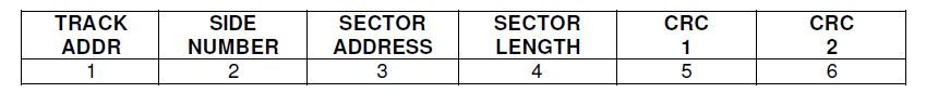
Tracks on a disk are laid down in the format:-
Track header...gap...(Track/Sector ID..gap..Data..gap) x N
times, ...End of Track
The Track/Sector ID consists of 6 bytes:-
Track#, Side (0 or 1), Sector#, Sector Size flag (,1,2,3
or 4) , and a 2 byte CRC check.
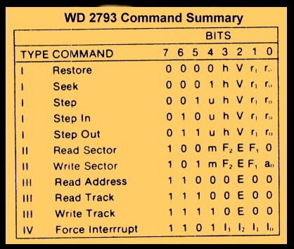
The command register accepts 11 different commands with very
precise bit patterns. They are summarized in this table.
First you will notice that the commands
are grouped into 4 groups.
The Type I commands
control the head movement. Bits 0 and 1 determine
how fast the head will move from track to track. For most modern drives the maximum
speed so these bits are 0,0. The V bit determines if the chip will verify
if it is on the correct track after the head to track movement is complete. Normally
a 1 but for disk formatting it is set to 0. The h bit determines if the head is
to be lowered on to the disk before or after the command function is complete.
The
Type II commands are clearly the most important (but the most complex).
Bit 0 of a Write sector 'a0' has to do with disk formatting and need not concern
us here and is set to 0.
F1 is another story. This bit simply determines if the chip is to check if the active head is reading
from the requested side of the disk. If 0 the WD2793 chip skips this side check. If
1 it checks that the active head is really on the requested side. The side of the
disk is contained in the Track/Sector ID field. The second byte of this field is
0 for side A (or a single sided disk). It is 1 for side B.
The E bit determines if there is to
be a slight time delay (15 ms) in setting the chip's busy flag after lowering the
head.
F2 on a WD2793 chip is relevant if F1
was set to 1 (enable side compare). If it is 0 the sector side field must
also be 0 (Side A). If it is 1 then the sector side field must also be 1 (Side B).
Finally the m bit allows you to read/write contiguous sectors on a track.
Very fast, but unfortunately difficult to incorporate in CPM BIOS code
because multiple sectors often are on different tracks.
The
Type III command either reads the
above track/sector ID field or a whole track. The write track command is primarily
for disk formatting.
The
Type IV command, force interrupt command
is to pull the chip out of a lockup situation. It's basically a chip reset command.
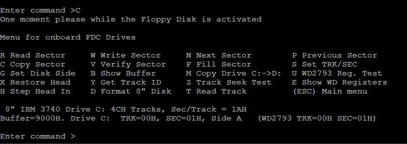
Use the Z command to bring up the monitor and
then use the
U command to bring up the Floppy disk menu.
(Please allow a second or two for the disk to come on).
It is this sub menu we will concentrate on for this board.
Let us go through the commands one at a time.
First add U3, U23, U6, U11 (a 74LS645), U21, U14, U12 (a 74LS645), U9 and
U20.
Add U19, U22, U17, U26, U25, U29, U28, U22, U1.
Add U8 and U13 (the DS1305 RTC Chip).
You can also add the four HEX displays.
Finally add the WD 2793 FDC chip U18.
At this point all IC sockets on the board should be full.
We will start calibration and
testing of this board by connecting a single 8” floppy drive, configured
as “Drive A”.
You also require an IBM
formatted single density floppy disk to perform these tests.
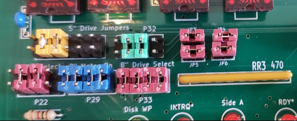
The following jumper settings
are for a pair of 8” drives (A: and B: ) and a 3.5” drive (C: ). These
settings will also work for testing with a single 8” drive attached:
P22: jumper pins 3-4, and 5-6
P29: no jumpers (Actully
does not matter).
Your 8” floppy drive should be
configured for stepper motor (spindle motor) “on” with “head load”. See
your floppy drive manual for setting this option on the drive.
P33: jumper 1-2, 3-4, 5-6, and
7-8. This allows the board to drive all 4 “drive select” lines to the
floppy drive cable.
JP3, JP4, JP5, JP6: These
jumpers force an active floppy drive “Ready” signal when the
corresponding drive has been selected. This is not necessary for normal
8” drive operation.
These jumpers are only necessary
for 5.25” or 3.5” drives that use pin 34 for a “disk change” instead of
a “ready” signal. However, in most cases putting a jumper on all 4 will
work fine.
P28: jumper 3-4 and 5-6. These
jumpers select the signals to 5.25”/ 3.5” drive pins 2 (“density
select”) and 4 (“in use”)
P32: jumper 3-4 and 5-6. These
jumpers allow use of a 5.25”/3.5” drive configured for use with a PC,
connected to a standard PC floppy drive cable.
K3 and P25: jumper K3 1-2 and
jumper P25. These selections drive the S100 “Ready” bus signal, which is
required by the IDE board but is not necessary for the floppy controller
board.
P20: these jumpers select signals to drive pins 48 and 50 on some very
old 8” floppy drive models. They are rarely required – consult the board
schematic if your drive requires these signals.
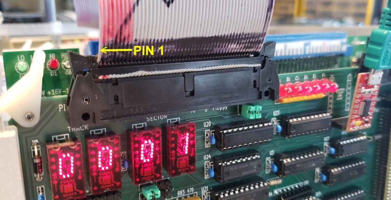
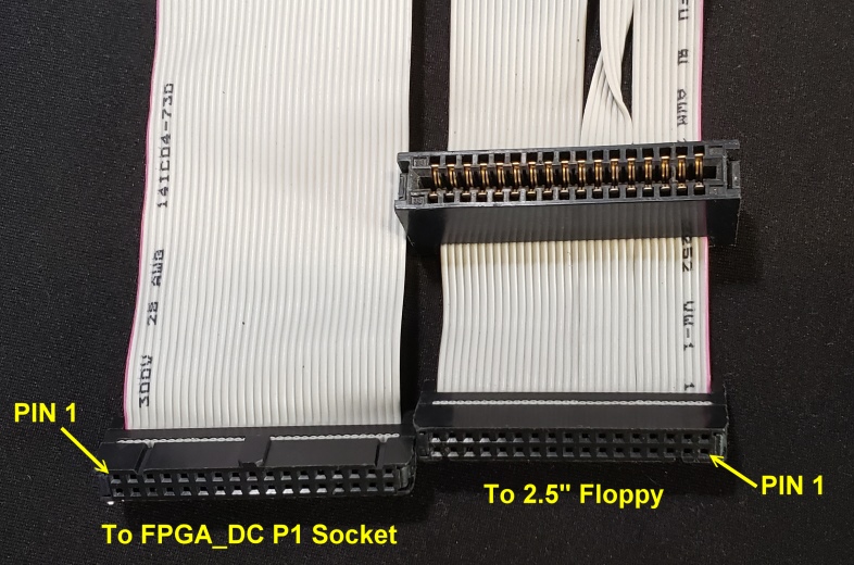
Hookup your 8" Floppy disk ribbon cable. Be sure you have the cable
correct. All signals are on the P9 connector even pins (top row). All
ground pins are on the odd pins.
Here is a close-up picture:-
The first thing we will do is check the WD2793 itself is receiving data from the
FPGA. With the "U" test we will continuously send Track and sector
data to the chips Track and Sector registers (Ports F1 & F2). We will read
them back. They must be the same. Here is an example:-
| |
 |
Next we will "Restore" the drive head to Track 0 (X
CMD). The Track 0 LED D15 should light up.
Then use the "H"
command to step the head in one track. Each time you press "H" you should
hear the head move. The Track 0 LED D15 should be off. The "X"
command will restore the head back to track 0 and the Track 0 LED should
come back on. This is a very simple test but it must work. It is completely
independent of the read/write drive electronics. Do not waste time going
further until you get this working. BTW, whenever the disk is rotating
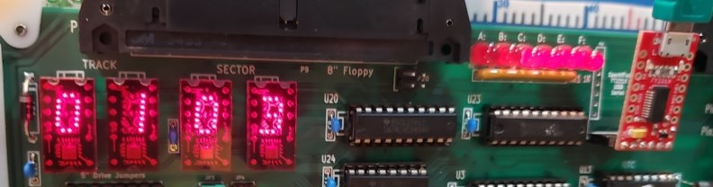
the IP LED (D16), should be faintly flashing. The Head Load LED
(D19) should light up also. For 8" Single Density Disks LED D18 should
not light up and the Side A LED D20 should be on and the 8" Disk LED D12
should be on.
Note also that LEDs D2 and D3 are RFU (so they will not
light up) however D4, D5, D6, and D7 will normally all light up.
Next we need to do actual disk sector reads and writes. Before doing this
however the
internal WD 2793 chip data separator needs to be fine tuned.
Adjusting the Data Separator setting of the WD2793.
One thing that often scares people away from these early FDC chips is the
need to fine tune the data separator/analogue signal of the raw data coming
in from the disk. I have found that the WD2793 works with almost
any setting for 8" single density drives. Not so for the double density 5"
floppy disks however. Early FDC boards often had elaborate hardware
that sometimes required careful adjustment to get a reliable signal,
particularly for Double Density modes. Western Digital greatly
simplified this process with the WD2793 chip. All that is required is one
50K Potentiometer and a 5-50pF variable capacitor. The
adjustment process is as follows:-
Reset the WD2793 chip (Reset on the S-100 system).
Start the boards Z80 Monitor program Z command.
Output
40H to Port
F5H.
Use
QOF5,40. This will set the WD2793
chip to double density mode, 8" disk. The LEDs D18 and D12 should be
on, (the others don't matter).
This should set the WD2793 pin 37 low and its pin 17 high.
Then
Jumper JP1. This sets the WD2793 "TEST" pin (pin 22) to ground. (It
will not work if JP1 is installed before the above reset).
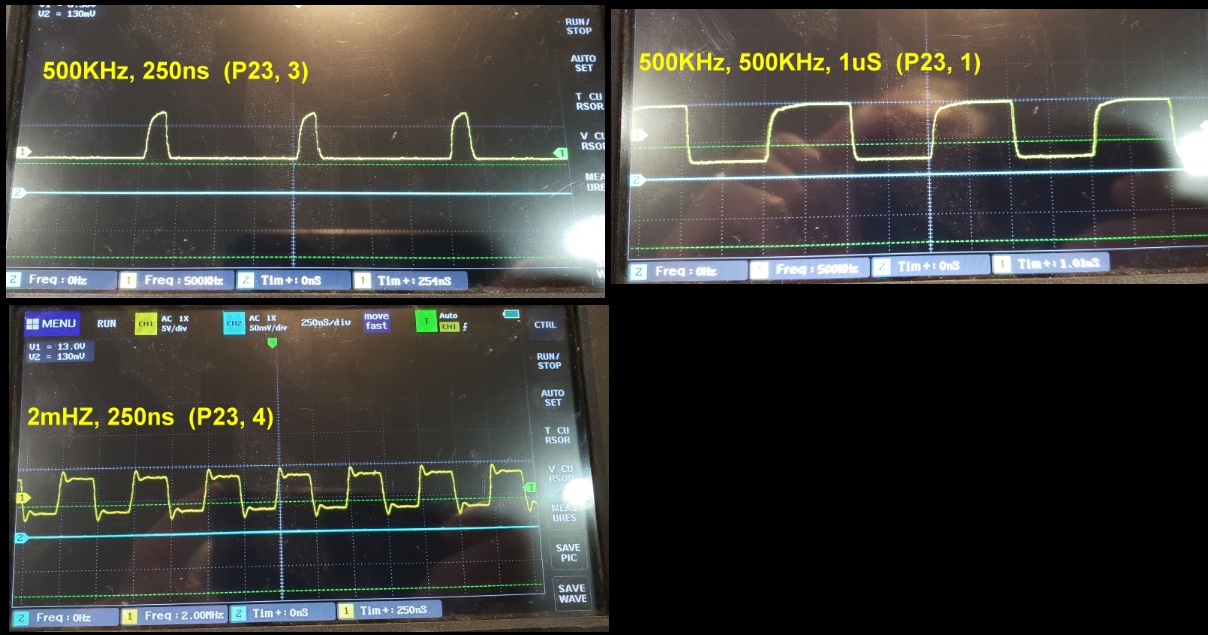
Then with a scope or logic analyzer observe the continuous
2mHz pulse on pin
24 of U18, or P23, pin 4.
Adjust the 50K pot on pin 18 (RV1) so the signal on U18 pin 29 or
P23 pin 3 has a width of
250ns.
Next adjust the variable capacitor (C12) so that U18 pin 16 (DIRC), or
P25, pin 1 has a width of
1uS
You
can use a scope, digital analyzer of simple handheld frequency counter.
When done be sure to remove the jumper on pin 22 JP1.
The
"Write Precomp Width" control Pin 33, does not seem to be critical.
I leave RV2 at about 25 KOhms. Try adjusting it if you get a lot or reseeks
while reading double density disks.
The above sounds more complicated than it actually is. In fact I have found
if the pot and cap are roughly in the middle of their range the chip works
fairly reliable. A poor man's approach might be to do continuous disk sector
reads and adjust things on the fly!
Below are pictures of my adjusted board using a
YEAPOOK ADS1013D digital storage analyzer. (An excellent machine BTW,
reasonably priced.)
When you are satisfied with the above settings, reboot your system
(remember to remove the JP1).
The following instructions require you have an 8”
IBM-format single-density disk inserted in the drive.
In the default mode the FDC menu comes
up with floppies B: & C: as 8" Single Density Single Sided disks.
Use the
"X"
Command to restore the head to track 0.
Use the
"H"
Command to step the head in one 1 track.
Then use the
"Y"
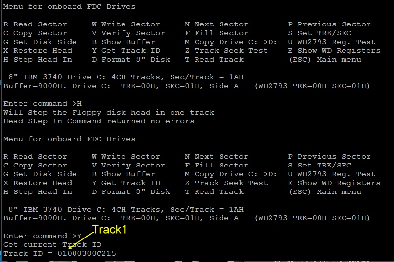
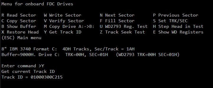
Command (Get Track ID) to have the WD2793 read the "Track ID".
This is
a very important test. It reads from the disk 6 bytes into RAM the "ID" of a
track. It can be any sector but it must be the correct track (01 in
this case)
Here is an example:
The format is:-
The first byte must be the correct track number. 01H in this case.
It is absolutely essential you get the
"Y"
command working before going father. It utilizes almost all the functions of
the WD2793 chip circuit.
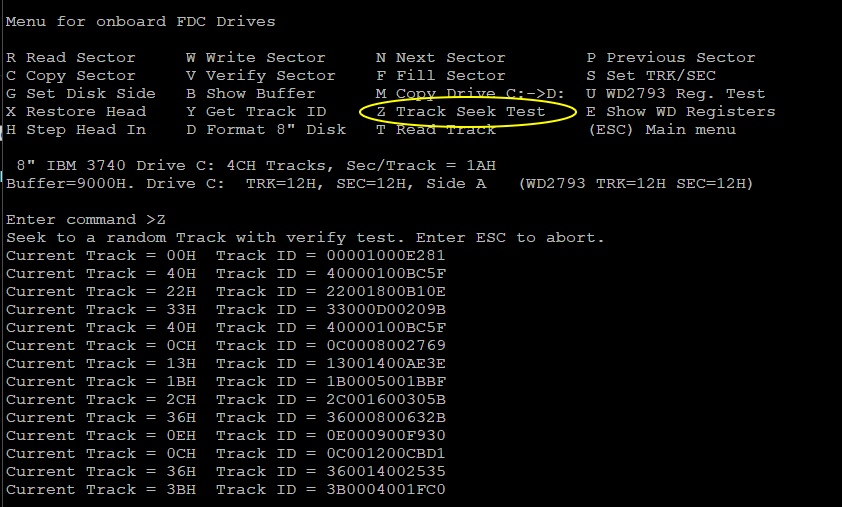
You can then move on to the "Z" Command that randomly seeks to different
disk track and reads the track ID.
The "Current Track" in the WD2793 register should always match the first
byte of the Track ID.
Here again is an example:-
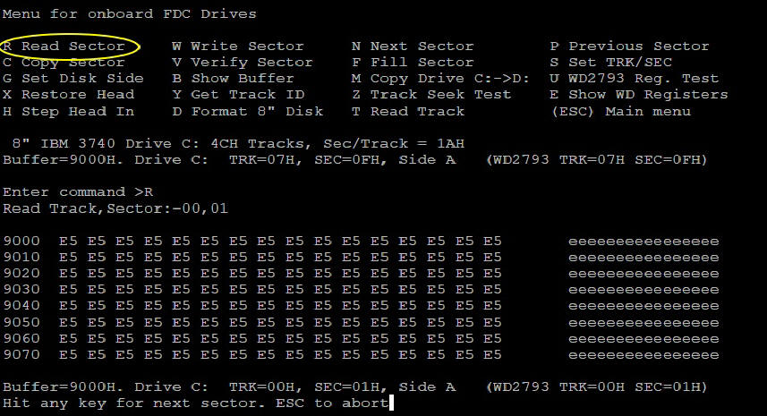
Next we will do an actual read sector. Start with Track 0, Sector 1, (There
are no 0 sectors on floppies). You should see something like this -- again
with no errors.
Hitting a CR will show the next sector. An ESC will drop you back to the
floppy menu. This test does require a properly formatted floppy disk!
The rest of the menu items are hopefully obvious.
If you have added the HEX LED displays they should be continuously updated
BTW.
The board will also accommodate 5" and 3.5" Floppy disks. They connect
via a ribbon cable to the connector P1.
Lets use a 3.5" drive. It's the most reliable and still reasonable common
these days.
You can format these disks on an old MSDOS PC. As far as the
WD2793 chip is concerned the format is an 8" drive,
Double Density, 80 (50H) tracks, 18 (12H) 512 byte sectors/track.
BTW, the Format command is also supplied in the
FDC_DIAG.COM program
(see below) and will also format these disks correctly with this board.
Making up a cable to these drives can be tricky/frustrating. I use the
common IBM-PC "twisted" floppy cable. Unfortunately you will probably have to
modify most that come with motherboards because they have a blocked pin hole
in the (motherboard) socket to prevent users putting them in the wrong way.
Here is a picture of the one I made up from a PC floppy cable.
Check Pin 1 as shown is connected at both ends. Note the cable wraps
around the top of each socket with a clamp to hold it in place. The
center notch for the FPGA socket must be as shown.
Likewise jumpers on the board for 5" and 3.5" drives can be tricky. On
the drive, set it as drive A:
Here are the board jumpers for 8" floppies and a TEAC 3.5" drive in C:
It looks somewhat messy in my S100 bus test system but here is the floppy
setup.
THE S100 BUS INTERFACE WITH THE FPGA_DC+FDC CIRCUIT
Having satisfied ourselves that we have the onboard hardware working
correctly we will now proceed to have the board interface with the S100 bus
as a true disk controller board.
That said, do not go to the S100 bus mode unless all the above commands work
flawlessly.
We essentially transplant the FPGA Z80 monitor disk
commands to the S100 bus. As we will see we elaborate on them to allow
multi disk transfers, reliability checks and anything else that assures us
the board can handle a CPM3 or MSDOS BIOS.
For debugging etc. I have written a Z80 program (FDC_DIAG.Z80)
that resides in the S100 bus RAM at 100H. It assumes the FPGA_DC ports
are 80H and
81H and the Console
IO is our
Propeller Console IO board (ports
0H
and
1H). Because it
resides at
100H it can be loaded
with CPM (later!), but for now you must download it from your PC via
a serial link and the Z80 Master monitor X command (X100).
By now this process should be familiar to most of our users. There are
other ways to do this, but in the end you need to have the
FDC_DIAG.COM (or
FDC_DIAG.HEX)
reside at 100H in RAM and jump to
100H from a Z80 S100
bus monitor.
First we open
Bit 7, (Pos 1) of SW1. This dramatically
changes how the FPGA Z80 operates after reset. The FPGA_DC
FDC board now comes up
in normal work mode. Initially its Z80 scans the S100 input port waiting to
receive a "Handshake CMD".
This is a
21H byte sent out on
the S100 bus to output port (81H).
It responds by echoing this byte back on
the S100 bus input port 21H.
With this the S100 bus Disk Operating system BIOS knows the FPGA_DC board is
alive and well. The two then continuously interact with other via
series of single byte commands. Normally this is done in your
operating system BIOS.
It will sign on as follows:-
After you select the drive you wish to work with the above menu will
appear.
As you can see this is a more elaborate version of the onboard FPGA monitor
commands.
Again most of these commands are self-evident. A number take one or more
follow-on single byte parameters. Some return to the S100 bus one or
more single byte values. In all cases they must return the
CMD_COMPLETE (F0H)
byte value confirming to the S100 bus BIOS that the requested operation
completed successfully. Anything else is regarded as an error and the BIOS
must act accordingly.
This CMD driven approach was first used with our
ZFDC Floppy disk controller board now
some 10 years ago! It turned out to be very successful and reliable
allowing a very simple CPM BIOS to access 8", 5" and 3.5" floppies is over
50 different formats with a few very simple set of byte commands. I used
the same idea we have here, the boards local Z80 does all the dirty work of
finding a sector on a requested drive given just the track and sector
number. In order to simplify the BIOS
software with all 3 boards in this series of FPGA_DC boards will use the same CMD format.
We will just add a few extra commands not found on the original ZFDC board
commands.
Here are the main commands for this FPGA_DC board:-
CMD$SEL$DRIVE
EQU 5H ;**** (Re)select an already initialized drive
CMD$SET$SIDE
EQU 8H ;**** This will set the active side for a
floppy disk
CMD$SET$TRK$SEC
EQU 35H ;Set new current TRACK+SECTOR on current drive
(new)
CMD$READ$SECTOR
EQU 10H ;**** Read data from the CURRENT sector (on
current track, drive).
CMD$WRITE$SECTOR EQU
11H ;**** Write data to the CURRENT sector (on current
track, drive).
CMD$HANDSHAKE
EQU 21H ;**** Handshake command only sent during board
initialization/testing
CMD$SET$IDE$MODE EQU
38H ;Set IDE drive hardware mode on FPG_DC Board (Internal
or External)
; Second Byte 0 = External IDE mode + Interrupt
driven info (Default Mode).
; Second Byte 1 = External IDE mode + CMD driven
info
; Second Byte 2 = Local FPGA Board IDE mode + CMD
driven info
CMD$FAST$COPY$AB EQU
39H ;Special CMD to fast copy CF Card A:->B: (All within
FPGA_DC Board software)
CMD$SET$HOME
EQU 0AH ;This will set floppy disk head request to Track 0
of CURRENT floppy drive
CMD$GET$TRACK$ID EQU
0FH ;Read the CURRENT FLOPPY TRACK ID
CMD$STEP$IN
EQU 0BH ;Step head in one track of CURRENT floppy drive
CMD$STEP$OUT
EQU 0CH ;Step head out one track of CURRENT floppy drive
CMD$SEEK$NV
EQU 0DH ;Seek to track with NO verify of CURRENT floppy
drive
CMD$SEEK$TRACK
EQU 0EH ;Seek to track to (IY+DRIVE_TRACK) with the track
verify bit set on CURRENT drive/format
CMD$TRACK$DUMP
EQU 15H ;Dump complete CURRENT floppy track to S-100
system
INFO$READ$SECTOR EQU
42H ;Send info, read sector (Actual Sec Read done
externally)
INFO$WRITE$SECTOR EQU 43H
;Send info, write sector
CMD$FORMAT$DISK
EQU 44H ;Format the disk in the of the CURRENT drive
CMD$FDC$COPY
EQU 45H ;Fast Copy Disk C:->D:
CMD$GET$TIME
EQU 80H ;Get Time and Data from FPGA DC Board RTC
CMD$SET$TIME
EQU 81H ;Set Time and Data on FPGA DC Board RTC
CMD$BOARD$CONFIG EQU
82H ;Get FPGA_DC Board hardware configuration
; Bits 7&6 contain IDE & FDC circuit flags
; Bits 1&0 contain IDE
For a CPM (or MSDOS) BIOS only the 5 commands in yellow are needed. The rest
are extra for testing and diagnostic purposes.
That said the commands absolutely have to be bullet proof and 100%
reliable.
The S100 bus OS BIOS does not know or care what type of disk is
talking to. It also has to be fast. There is a single 8 bit port bridge
between the two systems and a second status 2 bit port.
One subtle point for reading or writing to DD Floppy disks; Every now
and then the Disk Controller will get an error reading or writing a sector.
The Controller will simply try again. (Up to 3 times). The second try
is almost always a success.
A retry is flagged in the USB-TTY Terminal output by a "." character after
the CMD number (10H
or
11H).
Here is a part of an example for a CPM command:
PIP F:=A:*.*[V]
If you see more than say, 1 in 50 sectors reads or writes doing a retry,
try adjusting the WD2793 Double Density "Pump" resistor RV2.
For more information about this board skip to the software section
below and here
FPGA_DC Board Software.
Please note this FPGA “Floppty disk controller only”
board cannot be used in the same system as (a) an FPGA_DC+IDE board or (b)
any previous version of the dual ID/CF card board unless modifications
are made to the port selection logic of this board. The board is
intended as a stepping stone to the more complex FPGA_DC+IDE+FDC board
described next. The diagnostic software
described above can be downloaded from your PC via the Z80 master
monitor "X" command. it runs at 100H in RAM
The FPGA_DC + IDE + FDC Board
This board is essentially a combination of the above two boards.
Both the IDE and FDC circuits are on this board.
Absent unfortunately
(because of space limitations) is the Track/Sector LED Hex display.
The build instructions are exactly the same as is the software
from the two above boards.
As for the IDE & FDC boards you need to decide if you will use the 20 Pin DIP or
SMD version of the RTC chip (U13).
Solder in all the required IC sockets,
resistors, resistor arrays, capacitors, jumpers, and the Pololu 5V and 3.3V voltage regulators.
Read the instructions above about build the FPGA_DC+IDE Board. Do the same
thing.
Check the voltage levels for the socket pins are 3.3V and 5V. Be sure
the WaveShare 3.3v and 5V pins have the correct voltage before adding the
FPGA adaptor.
Here is a picture of the board at this stage:
For this board you can only use the "newer" IDE CF card adaptors.
There was not enough room with the old adaptors to fit in the CF cards
themselves without raising the board height and using two S100 bus slots.
With these adaptors you should also trim the pins protruding on the back of
the adaptor boards to get them closer to the board surface.
Because of the WD2793 associated resistors RV1 and RV2
and C12 board the IDE adaptors require a socket (P28, P32 or P10 &
P15) to keep the adaptor high enough off the board. See the discussion
on board height above for there FPGA_DC+IDE Board.
Try and use the Digikey (#S2141E-10-DD) right angeled connector series. They
have nice long pins on one side that allows you to adjust the adaptor height
above the board esaily.
Carefully directly solder U10,U15 and U16 to the board (using known good
chips). You may as well also add U20 and U21. Add the Waveshare FPGA Adaptor.
For this board we use a slightly different
.bdf
file to program the FPGA.
Upload the special project file FPGA_DC_IDE_FDC.qsf
on your PC system. Then
within the project load and compile the FPGA_DC_IDE_FDC.bdf
code
using Quartus.
Then power up the board and use the USB Blaster exactly as you did for the other two
boards to program the FPGA.
Be sure you download and open the file FPGA_DC_IDE_FDC.bdf
. The board will not run correctly with the
FPGA_DC.bdf
file.
Please also note the FPGA Z80 CPU runtime file
(FPGA_DC.Z80) is the same for all 3
boards. There is
no need to change that file for the
.bdf
file ROMs.
When the FPGA code is loaded the LED D10 (Board Active) must be flashing. Do not go further unless it is.
You must get this LED flashing display before proceeding further.
First we will add the IDE/CF card section and
test it out.
First be sure the is no Dual IDE/CF card board (or either the FPGA_DC+IDE or
FPGA_DC_D+FDC) in the bus.
Install the following IC's:-
U2, U4, U7, U9 and U12, Remember U12 is a 74LS645 or at
least a 74LS245.
Add U1 and the RAM chip U5.
Jumper
K5 1-2
and
K4 1-2. This will activate both the IDE
ansd FDC circuits
in the FPGA
Jumper K1 1-2, and Jumper P25
IEEE-696 16 bit S100 bus port IO addressing is assumed (the upper 8 lines
being zero) for this board. This can be easily bypassed within the FPGA
(Jumper K1 1-2). Do so if your CPU board does not zero the high
address lines for port I/O. To be safe we will jumper K1 1-2 for now. Note
16 bit CPU's will probably require K1 2-3.
Install the Sparkfun
FT231x USB adaptor. Note it has a jumper on its back for 3.3V operation,
use 3.3v not 5V. You can
solder the adaptor directly to the board or use sockets. See the
section above on soldering sockets. I suggest direct
soldering. Note the USB FT231x adaptor actually has 3 sockets. The two side ones are not used here and are
only there to steady the adaptor on the board. I use only pin 1 in each
case. You can also use the
Adafruit CP2104 USB adaptor equivalent adaptor. Perhaps it's just me, but sometimes
I've
had problems getting this adaptor to link up with my PC's.
Please note if you use a ribbon cable connector socket with ejectors
(recommended), then the USB adaptor is a very tight fit.
The default software on this board assumes a USB port running at 38,500 BAUD, 2 stop bits, no parity.
(This can be changed within the FPGA_DC.bdf file). There are a number
of Windows/PC programs you can use to receive and display the data. I
like
Absolute Telnet
from Celestial Software, but others are free.
The board has an "IOBYTE" switch (SW1),
which defines what the FPGA_DC Z80 monitor
does on power up. The default mode, all switches open, (no switch) causes
the Z80 monitor to get
0FFH
from port
46H after a reset. This is the boards normal mode of
operation but we will not use it yet. Currently only two
switches are utilized:-
Bit 0 (Pos
8), (Reading left to right), when closed, (xxxxxxx0H),
this causes the board to send status information to the USB port during
every step of its operation. A remote PC can thus watch how commands sent
from the S100 bus are operating during "disk" operations. This slows down
the Operating System BIOS a little but is invaluable for debugging etc. When
open no commands are sent.
Bit 7, (Pos1),
when closed, (0xxxxxxxH),
this causes the board upon reset to bypass the S100 interface and go
directly to its onboard monitor. The onboard monitor contains all the
"normal" commands for a Z80 CPU, display/change RAM, ports etc. but it also
contains two very special command I
and
U.
Place the board in the S100 bus with
SW1 positions
8
and
1
closed. Power up and again load the
FPGA_DC.BDF
file into the FPGA. Upon reset the FPGA will boot up its Z80 monitor.
You
should see the following display:-
For now just use the Z command. This will bring you directly to the
FPGA Z80 CPU monitor. You should see the following:-
Most of these commands should be familiar to our users. (The
X command BTW,
is not yet implemented).
Play around with the regular Z80 monitor commands (except
I,
U and
X)) at this stage to get
comfortable with the interface.
For example the A command will show
you the "Memory Map" for the Z80 on the board.
You must get this monitor display working before going further.
Here is a picture of the board at this stage:
Next add U11 (a 74LS645) and U14.
U20 & U21 should already be in place. Add U1.
Add both IDE/CF card adaptors with their sockets. Remember the newer
adaptors go in sockets P10 and P15 (with Pin1 on the RHS).
Add U26 (I have had a number of CF card initialization problems with some
82C55A's e.g. NEC and OKI chips. The only reliable chip I find is the
NEC 82C55AC-2).
Use this (common) chip.
Here is a picture of the board at this stage:
Boot up the board as before and bring up the IDE disk menu for Drive A:
You should be able to access both drives with all the commands as you did
for the
FPGA_DC+IDE Board
described above.
Next we will add the FDC card section and
test it out.
Remove the IDE adaptors for now.
Install the following IC's:-
U3,U6, U17,U19,U30,U24,U22,U23,U25,U27,U28 and U29.
I have a 74F244 for U6. You can probably use a 74LS244 however.
Add U8 and U32
Add the WD2793 U18 chip.
Make sure jumper K5 is 1-2 (and K4 1-2).
Jumper K2 2-3
You may as well add the RTC chip at this stage also. We will test it later.
So add U13, (either the DIP chip or SMD chip).
Also add a 3V Coin battery.
Here is a picture of the board at this stage:
Insert the board in the S100 bus and connect a Floppy Disk cable. If
possible start with an 8" drive.
Power up the board and upload the FPGA_DC_IDE_FDC.BDF
code for the FPGA.
Make sure SW1 has bits 7 and 1 set to 0. The board should signon
as follows:-
Ignore the fact that unconnected drives are "initialized" for now. The LEDs
for C:, D:, E: and F: should light up however.
As for the
FPGA_DC+FDC
board described above launch the Z menu and then the
Floppy menu and checkout U,H, and X commands.
You must be able to move the head etc. before going further.
Next we need to optimize the FDC data separator. This is done exactly
the same way as you did for the
FPGA_DC+FDC board
see above.
When you are satisfied with the above settings, reboot your system
(remember to remove the JP1).
In the default mode the FDC menu comes
up with floppies B: & C: as 8" Single Density Single Sided disks.
Use the
"X"
Command to restore the head to track 0.
Use the
"H"
Command to step the head in one track.
Then use the
"Y"
Command (Get Track ID) to have the WD2793 read the "Track ID".
This is
a very important test. It reads from the disk 6 bytes into RAM the "ID" of a
track. It can be any sector but it must be Track 1.
Here is an example
The format is:-
Continue everything else exactly as you did for the
FPGA_DC_FDC Board
above. The core FDC circuit is almost identical in boards. The only
major difference is the WD2793/FDC circuit has its own data buffers to the
FPGA Z80.
The IDE circuit uses U11 and U14. The FDC circuit uses U8 and U32.
I found the separation lead to a much more reliable setup. There
are a number of other optimizations as well -- thus the different
.bdf
file.
Here is a picture of the finished board:
Board Height.
One problem with the +IDE+FDC board is that the board takes up the
space of two slots in most S100 buses. Probably OK for most
people anyway since it does the function of two boards anyway.
There is a way to get around this however. If you solder the IC's in
the area shown here directly to the board you can place the IDE adaptor
closer to the board surface.
However you need to very carefully attach the IDE adaptor pin array to the
board. I managed to locate special 20X2 right angled pin headers that
are extra long on one side:-
This allows you to nicely adjust the adaptor above the board. You trim the
pins on the back afterwards. Unfortunately I can no longer locate the
source. The "regular" right angled headers do work but they
should barely show on the back of the board to get the right height. BTW the long
straight section of these must go into the IDE adaptor. The angled section
into the board.
There is another board height issue. The programming socket of the
Waveshare FPGA adaptor also prevents the board fitting into a single S100
bus socket.
For most motherboards you can handle this by trimming the plastic shroud
around the programming socket. See here:-
It may be necessary to snip a little off the top of each pin as well.
A more elegant solution is to replace the above socket with a right angled
one. This I only recommend to expert solders. Heat each socket
pin on the back of the socket and with a tweezers pull it straight out when
it is hot. It must be quite hot and come out easily. If not, you will
rip off the attached PCB trace to the pin. Clean out the holes (10)
with a suction desoldering gun and insert a right angled 5X2 header socket
as shown above. I was almost reluctant to suggest this approach. Only
use it 1, after a final programming of the FPGA and 2, you are an expert in
soldering and desoldering.
Hardware/Software Debugging.
These are relatively complex
boards. Things are complicated by the fact that much of the circuits reside
within the FPGA. However I have split the
FPGA_DC.bdf
file into discrete sections such as the Z80/ROM
section, the serial/USB port section, the SD cards section, the IDE/CF card
or FDC
sections etc.
There are three basic levels of difficulty:-
1. You cannot get to the main menu of the onboard Z80 monitor
2. Some of the SD/CF card or FDC routines don't work correctly
3. The S100 interface does not work correctly with the board.
Option #1 difficulties are the most serious. Most lightly they are due to a
bad solder joint, a bad IC socket or IC, or an incorrect placement of the
latter. A key flag is if the "Board Active" LED (D10)
pulses when the FPGA is programmed. If this does not occur rip out
every IC on the board except the FPGA adaptor. If it still does not work you
have either a power problem a faulty Cyclone IV adaptor or a programming
problem. If you have a flashing LED, then step things along adding one
IC at a time.
If you have a flashing LED
D10 you might next suspect the FPGAs
access to the onboard RAM chip (U5).
See if the RAM read/write pins are pulsing. The address lines are changing
and the data lines are pulsing.
Next up is to suspect your Serial/USB port adaptor interface. If you
have another board with a similar serial/USB port check your PC can interact
with it at the same
38500 BAUD.
If it's OK check you are seeing the LED on the Adafruit adaptor pulse as it
sends data to your PC.
If these are OK you may need to modify the code for the FPGA Z80.
Bring up the
FPGA_DC.Z80
file. You will see :-
;
H_TEST1 EQU FALSE
;For initial hardware debugging
H_TEST2 EQU FALSE
H_TEST3 EQU FALSE
One at a time set the
EQUATE TRUE. For example setting:-
H_TEST1
EQU TRUE
you should see an
'@'
character on the USB Port/PC TTY windows
terminal. Step things along within the monitor code to determine where
the problem is.
Remember the board must work 100% reliably in local mode before you activate
the S100 interface
(SW1-8
closed, bit 7 = 0).
If you run into #2 problems with the SD or (less lightly) CF cards your
first option should be to reformat the cards in windows. Failing that,
try a different card. It appears all these cards don't behave the same
-- particularly initializing the SD cards. You will have better luck
with the older (a few GB)
Type II cards than with the new very high capacity cards. Here is a
picture of three common cards I use that
are 100% reliable with these FPGA_DC Boards.
I have also found that some mini SD cards do not work using the SD->CF card
adaptor. However as best I can tell all (e.g. Samsung) Micro-SD cards
(themselves in a Micro->Mini SD adaptor) work well in the SD-->CF adaptor.
Type #3 problems tend to be the easiest to fix. They will center
around the four port bridge interface between the FPGA_DC board
software/hardware and the corresponding S100 bus. First be absolutely
sure you do not have any other board in your system using ports
80H & 81H
The board assumes IEEE-696 signals for
pSYNC, pDBIN, sINP, pWR* and sOUT.
Also address 16 address lines and the 8 data in and out lines. 16
bit port IO addressing is assumed (the upper 8 lines being zero), though
this can be easily bypassed within the FPGA (Jumper K1 1-2).
In every case you can step the FPGA_DC board along by simply sending one
command byte at a time to out port
80H,
wait for the acknowledge byte to come back on the in port
80H.
Long term users of the IDE/CF board will remember that there was an issue
with CPM BIOS code and the assigned sectors/track format (see
here). To recap, it was originally
written for use with the board and a "real" IDE hard disk, a
Seagate Medalist
6531 ULTA ATA drive. This was a fairly popular drive at the time (1998),
and is still often seen today on eBay. It had 13446 cylinders, 15 heads and
63 sectors/track, (6.5 GB Capacity). In order to have only one CPM3.SYS
image on all disks and all CF cards we used a format of
61 sectors per track (with the possibility if
need be, to use the spare sectors if needed for bad sectors). This
complicates the BIOS unnecessarily. Some changed the format to
6F sectors/track. Somewhat better.
For all CF and SD cards here, we will use 0FFH sectors/track. This is
the default table in the current FPGA Z80 code. However to
working with files for the two "old formats", the FPGA Z80 code can be modified
with
SW1 bits 1 & 2 for drive A: and B: as follows:-
SW1
xxxxxx0x FFH tracks,
3CH
sectors per track for IDE/CF drive A: and B:
SW1
xxxxx0xx FFH tracks,
3FH
sectors per track for IDE/CF drive A: and B:
Please note this designation is only activated with a board reset when each
CF card is initialized (or by pressing the reset button SW2 on the board).
This option is only rarely used,
it should be
used with extreme care remembering the "old formatted" CF cards
must have been written
with a CPM BIOS of
3CH
or
3FH
sectors/track. Note this really only speeds up disk copying etc. The FPGA
software is completely independent of the disk BIOS software. Normally you
will use 0FFH sectors/track -- its just some sectors will not be used by the
BIOS.
The initial drive selection menu will always show you the current IDE drive
format assumed by the FPGA Z80 code:-
LED's
These
boards have quite a number of LEDs. Lets go through them one at a time.
The FPGA_DC+IDE Board
The 6 LEDs (D2, D3, D4, D5, D6, D7)
are on all 3 boards. On this board only
D2 and D3 (Labeled
C: and B:) are utilized in the current FPGA Software. They light up AFTER an
IDE Drive/Card is fully initialized on power on. They should then stay
on all the time. They are NOT Drive select LEDs. If either LED does
not light up there is a problem with the drive/card hardware.
The two LED's D12 and D1 (beside the IDE Adaptors) are true
Drive Select LEDs, that
come on when a R/W drive is active.
The two S100 Status LEDs
D8 and D9 flash
when data travels to/from the S100 bus. These are really only there
for debugging purposes.
Finally the
FPGA Active
LED D10 should
always be flashing. Its there to show the FPGA is active. If it does not
flash something is seriously wrong with the FPGA code.
The FPGA_DC+FDC Board
The 6 LEDs (D2, D3, D4, D5, D6, D7)
are on all 3 boards. On this board only
D4, D6, D7 and D7
(Labeled C: to F:) are utilized in the current FPGA Software. They light up
AFTER a Floppy Drive is fully initialized on power on. They should
then stay on all the time. They are NOT Drive select LEDs.
The two S100 Status LEDs D8 and D9 flash
when data travels to/from the S100 bus. These are really only there
for debugging purposes.
Finally the FPGA Active
LED D10 should always be flashing. Its
there to show the FPGA is active. If it does not flash something is
seriously wrong with the FPGA code.
There are some key WD2793 FDC related LEDs:-
D13 lights up if the
current Disk Drive software wishes to inform the user that the current disk
is write protected. It's the responsibility of the BIOS software to
determine this by looking at the WD2793 status register. Bit 6 will be 1 if
a disk is write protected.
D22
will flash each time the WD2793 triggers its INTRQ*
pin 39 (or each DRQ* Pin 38). Which one is determined by Jumper K4
(1-2 = DRQ, 2-3 = INTRQ)
D20 will be on if
side A of a disk is being accessed.
D17
will be on if the current disk drive indicates its
ready to operate (P9 pin 22 or P1 pin 34 from the drives themselves).
D12 will be on if
the WD2793 is configured to be talking to an 8" drive.
D21 is really for
debugging purposes to indicate the FPGA is waiting to break out of a loop
during a sector read or write by an interrupt.
D15 will light up
whenever the current disk head is on Track 0.
D18 will light up
if the WD2793 is configured to be talking to a double density drive.
D19 will light up
whenever the drive head is lowered on to the disk surface.
D16
will flash whenever the disk index hole is detected during a disk rotation.
The IDE and FDC boards have two jumpers
Test_1 and Test_2. These are TTL level
outputs from the FPGA than can be used for debugging the Z80 software.
Unfortunately there are no spare FPGA pins on the IDE+FDC Board.
Burning FPGA Code to Flash RAM
Up until now whenever we programmed our FPGA via the JTAG
socket an the above boards the data is lost whenever the power is turned off. While
fine for code development etc. it is not desirable for a final board
configuration. Like most FPGA applications the "final" code is saved
in Flash RAM and immediately loaded by the FPGA each time upon power-up.
This is a standard and common characteristic of most FPGA's. Some older
models in fact had a ROM onboard. Our Cyclone IV Adaptor
board has 16MB of Flash RAM on board for this purpose -- way more than we
are ever going to need!
The tricky part is programming this Flash RAM. I found the
Intel documentation poor and confusing. Here is a summary of the process:
Within Quartus you need to "convert" your normal JTAG FPGA
.sof
programming file
to a special file
.jic
to program the Serial Flash RAM chip on the Weveshare
board.
Within Quartus, click on the File Menu and select "Convert Programming files".
The dialog box below will popup.
From the dropdown box on the "Programming
File Type" select a
.jic
file type.
This is the file format that is required to program the onboard serial Flash
RAM.
For the
Options/Boot
info select
EPCS16.
Leave
Active Serial as is.
You can name the
.jic output file anything you like. I usually just leave it
output_file.jic.
Note it will be in the Quartus generated "output_files"
folder within your work directory.
Next click on
Flash loader
within the lower "Input Files to
Convert", then click on the highlighted "Add Device"
button.
You will get a popup dialog box as shown below.
Select
Cyclone IV
and
EP4CE10.
Note
Quartus takes some time to allow you to actually select
these options -- seems to be doing things in the background!
Next click on "SOF Data"
and "Add File".
You should see your "normal" FPGA program
.sof
file in your "output_files"
folder within your work directory.
Finally click the "Generate"
button.
You should get a popup dialog saying "Generated
output_file.jic
successfully.
Note the name and location of the converted file. Then close that dialog
box. See the pictures below.
Next we need to actually flash the Waveshare boards RAM chip.
Click on the normal "Program Device (Open Programmer)" you normally use. If
its not already open, give it time to come up as a dialog box.
Make sure your board has power. To be safe click the Auto Detect
button. your normal xxx.sof
file should display with the device set as
EP4CE10F17.
First delete the "FPGA_DS.sof
| EP4CE10F17...."
line
etc.
Click on
Add File
and select the
xxx.jic
file you just generated above.
Click on the Program/Configure little square character boxes.
The chip diagram below should show only 2 chips as shown. If more, right
click on any 'extra' one and delete it. The dialog box must look as shown
below.
The
Start
button should highlight.
Click on this and you will flash the RAM chip. Follow the Progress bar
until it is done -- it takes about 1 minute.
You can power off and re-power your computer.
Your FPGA board should (after reset), start with whatever FPGA code is
within the chip.
Note when you close the above dialog box, normally you do NOT save the
changes.
Typically you want the chip to be quickly reprogrammable for testing etc.
Installing Quartus Lite on Windows.
In spite of its name the
Quartus Lite IDE is a
large program. When fully installed the Quartus folder is over 15GB in
size. Installing it makes Microsoft's Visual Studio seem lightening
fast!
That said, its an excellent IDE. Figure on 1 hour to install and
get it right. For our purposes we will only be using probably 5% of
its capabilities, but I have found if you try and get smart by not
downloading or removing sections you run into problems later during usage.
Please see
here for instructions on how to install Quartus.
Software
The
software for these 3 boards is fairly complex. There is no way around it,
to accommodate the wide verity of cards and disks possible. In theory at
least most beginners should not have to alter the software at all. To
facilitate the installations all three boards use the exact same software
(both within the FPGA and the
IDE_DIAG.COM
and
FDC_DIAG diagnostic programs). In fact
the CPM
IDE_DIAG.COM will also work with the old
IDE/CF board. I should also mention that the current software is
nowhere near allowing these boards to attain their full capacities.
Currently for example only a few Floppy disk formats are covered. The
ZFDC Controller Board still currently
stands as the better board in this respect. That said, there is no
reason why any soft sectored floppy, IDE drive, CF or SD card cannot be
utilized by this board. You should have fun modifying the code to do
so. I have made a special effort to extensively comment the sections.
Here is how the
FPGA_DC.Z80 code is structured:-
Program Equates
Setup Stack and Interrupts
Move the Drive Tables from ROM to RAM
Initialize the IDE Drives and Tables
Initialize the Floppy Drives and Tables
Check IOBYTE Port to see if a jump to the Z80 Monitor is required
Enter the main program Loop (START_CMD:)
Process each Command sent from the S100 Bus
The Commands code
Code to update the HEX LED Display
Code to send Info to the USB Terminal
The Z80 Monitor Menu and code/loop
The Local IDE/CF Card Menu and code/loop
The Floppy Disks Menu and code/loop
Core WD2793 Routines
General software support routines
Core IDE Drive Routines
Real Time Clock routines
Disk parameter tables
Menu strings
ASCII Text/messages
RAM variables (starting at 9000H in RAM).
Remember if you do modify the above code be sure Quartus knows where the new
ROM
ZFDC.HEX file is
located when compiling the ZFDC_DC.bdf
file.
Likewise the Quartus
FPGA_DC.bdf file
is fairly well structured. The FPGA board "components" are layered top down
as follows:
Clock Generator
Z80 CPU module
S100 Address Lines and key signal inputs
Internal Z80 Bi-directional data bus
RAM interface & ROM Module
UART Interface
IO Ports and Switches
Local IDE Interface
External IDE Interface
S100 Bus Interface
Floppy Disks interface
Hex LED Display circuits
S100 Bus bridge to FPGA Ports
SPI Real Time Clock Interface
Accessing the FPGA_DC Boards from the Z80
Master Monitor.
For a quick check of these FPGA_DC board(s), I have now added a new command
to our Z80 Master
Monitor. This is the "Y" command.
The code resides in the second ROM page of the monitor. Please see
here for a
write-up
of this dual 4K page monitor.
While the list of menu options is small it does show how with a few 100
bytes of assembly language code one can initialize and R/W sectors from any
IDE drive, CF or SD Card or Floppy Disk (8", 5" or 2.5").
Installing CPM3 On The FPGA_CF Board.
For this Disk Controller card to be of any practical use we need to install CPM
(and later, other disk operating systems) on drives interfacing to it.
We could start with CPM version 2.2, but it is actually far easier to write a
BIOS for CPM3 because CPM3 takes care of buffer sizes greater than 128 bytes
internally (all IDE and SD drive sectors are 512 byte sectors) and is in general is a
more practical and expandable system.
I should add if somebody wants to use CPM V2.2 for the IDE version of the
board you only need to change the
Disk Parameter Table to 128 byte sectors (instead of 512) -- wasteful, but
"drive" capacity is never an issue here.
Before writing a CPM3 BIOS for this board please read the write-up I
have in the software section of this site about setting up a CPM3 system on
a floppy disk system and the original IDE/CF Board.
Please read
here and
here.
If you have written a CPM BIOS before you will find hammering one into
shape for this FPGA_DC board is in fact fairly easy. If you have not
written a CPM3 BIOS you will have to spend some serious time studying the
above web pages.
To get people going I have include a basic CPM3 BIOS that assumes just a
Propeller Console IO board
for Console I/O and this board.
I have include a program
HSYSGEN.Z80
to write the built Digital Research CPM3 operating on to the IDE/CF Drive #3
or #4 system tracks.
This CPM3 BIOS assumes only 2 drives. Two CF or SD cards,
no floppies, printer etc.
Please go to the software section of this web site for instructions and
relevant files for Install CPM3 on the FPGA_DC
board.
Source of chips
Most of the IC's use on this board are common 74LSxx chips available from
numerous sources such a Jameco, Mouser & DigiKey.
A great source of older chips is
Unicorn
Electronics who have very reasonable prices - though chips are hard to
find on their web site.
The FPGA_FDC board requires the Western Digital Floppy
Disk WD2793 controller chip. Unfortunately
it is not too common. It was used in some old
Atari systems from which it can be easily pulled. The chip can from
time to time be found on eBay. It can also be obtained locally here in the San
Francisco bay area at
Anchor Electronics. They take phone orders.
The TIL 311A's are
expensive (~$20 each from places like Jameco). However overseas
outfits like
Utsource sell them in small quantities for ~$4 each. Utsource have about
a 1 week delivery time to the US since they use DHL. They also appear
on eBay. It is indeed
frustrating these LED HEX displays are so expensive. With the exception of
the even rarer HP-5082's
other such displays display only the digits 0-9. There is not enough room
on the FDC board for the
FPGA_DC+IDE board Hex
Displays. The board BTW works fine without them.
Software for this board.
Over time I anticipate a fair amount
of software for these boards, so I have setup a separate web page for all
FPGA_DC Board related software here:-
FPGA_DC Board Software
All the links below in fact go to that page. There is a step by step
description of how to get a basic CPM3 system running with two CF cards.
If you develop software
for these boards please send it to me and I will post it there.
Bugs
In the BOM for the IDE board the quantity for “LED, Red Diffused,
643 nm, 65mcd, T-1” should be 8, rather than 3.
In the BOM for
“628512LP-70, SRAM, Asynchronous Memory, 4Mb (512K x 8), Parallel, 70ns,
32-PDIP” [Jameco 157358 $12.95] a significantly less expensive alternative
is an AS6C4008-55PCN from Mouser [$6.24]:
https://www.mouser.com/ProductDetail/913-AS6C4008-55PCN
I'm still having problems booting CPM using non-
NEC 82C55AC-2
chips on the FPGA_DC+IDE Board!
By accident I popped in an OKI M82C55-2 and later a AMD P8255A-5.
Neither of the latter two chips worked reliably booting CPM3. It seems
to be related to the age old problem we have had with these IDE/CF cards
from the beginning, namely the shape/length of the card initialization
reset pulse.
Several times I thought I solved the problem only to have it reappear
later. It's definitely go to do with the timing of the
initialization Reset pulse to the CF cards.
Perhaps somebody else can experiment/solve the problem. For now,
please use the NEC chip.
Earlier versions of the software for the FDC (only) FPGA_DC Board would
not work with the Dual IDE/CF card in the bus. There was a
conflict with the same port addresses on both boards.
This has now (12/2/2021), been corrected. Be sure jumper K6 is set 2-3
(LOW), the IDE circuit on the FDC board is then inactive (as it should
be).
Error on the FPGA_DC +FDC Board
For the FPGA_DC + FDC Board there is a minor Silk
Screen error under the connector P1.
It should read '3.5" Floppy Connector'
not
2.5"
Error Compiling the FPGA_DC
+IDE +FDC Board
Henry Broekhuse has noted that he could not get the files in the
FPGA+IDE+FDC folder to compile. Quartus could not find certain Z80
module files.
The way around this he suggested is:-
1. Start with the folder of files for this project,
as provided in the ZIP FPGA_DC_IDE_FDC.ZIP
2. Start Quartus, open the QPF file for this project,
then the BDF file for this project.
3. In the menu bar, click on Project, and from the
drop-down select "Add/From files in Project"
4. In the box that pops up, add the following files
to the project (they are all located at the root level of the folder for
this project):-
T80_Pack.vhd
T80_MCode.vhd
T80_ALU.vhd
T80s.vhd
T80.vhd
spi_master.vhd
spi_16bit_master.vhd
Microcomputer.vhd
... then click Apply, and OK
The project will now compile correctly.
Board Layout
Some of the above pictures of the above (prototype) boards have a
slightly different layout to the final "production" board. The actual
schematic however is unchanged.
To Order a Production S-100 Board
Realizing that a number of people might want to utilize a
board like this together with a group of
people on the
Google
Groups S100Computers Forum, a "group purchases" was formed. It is now closed.
Please see here
for more information. Please do not contact me directly.
Please note some of the above pictures of the boards during the build
process are late stage prototypes. The position of certain items may be
slightly changed from the final (V1.0) versions.
The links below will contain the most recent schematic of the above boards.
Note, it may change over time and some IC part or pin numbers may not correlate
exactly with the text in the article above.
FPGA_DC + IDE BOARD
FPGA_DC
+ IDE Board Schematic (V1.0 IDE Only) FINAL .PDF File (8/27/2021)
KiCAD files for FPGA_DC
(V1.0 IDE Only) FINAL .ZIP File
(8/27/2021)
Gerber files for FPGA_DC
(V1.0 IDE Only) FINAL .ZIP File (8/27/2021)
BOM of FPGA_DC+IDE Board (PDF File) (8/22/2021) Contributed by Rick Bromagem
BOM of FPGA_DC+IDE Board Excel File)
(8/22/2021) Contributed by Rick Bromagem
Board Layout of FPGA_DC+IDE Board (PDF File) (8/22/2021) Contributed by Rick Bromagem
Quartus FPGA_DC .BRD Folder
(12/2/2021) Files to program FPGA
(for IDE or FDC Boards only. Not the IDE+FDC Board)
FPGA_DC + FDC BOARD
FPGA_DC
+ FDC Board Schematic (V1.0 FDC Only) FINAL .PDF File (9/12/2021)
KiCAD files for FPGA_DC
(V1.0 FDC Only) FINAL .ZIP File (9/12/2021)
Gerber files for FPGA_DC
(V1.0 FDC Only) FINAL .ZIP File (9/12/2021)
BOM of FPGA_DC + FDC Board (XLS File) .XLS
File (11/1/2021)
Contributed by Henry Broekhuyse
BOM of FPGA_DC + FDC Board
KiCAD BOM Listing
.CSV File (10,25,2021)
Board Layout of FPGA_DC+FDC Board (PDF File)
.PDF File
(10/25/2021)
Quartus FPGA_DC .BRD Folder
(12/2/2021) Files to program FPGA
(for FDC Board)
FPGA_DC + IDE + FDC BOARD
FPGA_DC
+ IDE+FDC Board Schematic (V1.0 IDE+FDC) FINAL .PDF File
(10/25/2021)
KiCAD files for FPGA_DC
(V1.0 IDE+FDC Only) FINAL
.ZIP File (10/25/2021)
Gerber files for FPGA_DC
(V1.0 IDE+FDC Only) FINAL
.ZIP File (10/25/2021)
BOM of FPGA_DC
+ IDE + FDC Board BOM (PDF File) .PDF
File (1/29/2022) Contributed by Rick
Bromagem
BOM of FPGA_DC
+ IDE + FDC Board BOM (XLS File) .XLS
File (1/29/2022) Contributed by Rick
Bromagem
Board Layout of FPGA DC+IDE+FDC Board (PDF File)
.PDF File (1/29/2022)
Contributed by Rick Bromagem
BOM of FPGA_DC+IDE+FDC Board Excel File) .XLS
File
(1/31/2022) Update Contributed by Henry Brekhuyse
Quartus FPGA_DC_IDE_FDC
.BRD Folder
(12/18/2022) Files to program FPGA (for IDE+FDC Board
only)
Please go to the FPGA_DC Software page for all runtime programs
FPGA_DC Software
Other pages describing my S-100
hardware and software.
Please click
here
to continue...