On Sat, Mar 1, 2014 at 7:39 AM, Crusty OMO <crus...@hotmail.com> wrote:
Hi Paul,
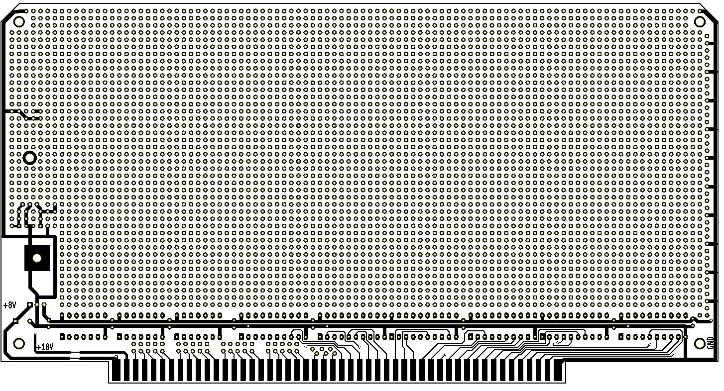
Have you never lost an LED at sea? hehe, just kidding. The idea is to be at the top of the card cage, some S-100 systems pack the cards in pretty tightly. The single trace out to sea does look out of place... but you'll not really notice it on the actual board after it's covered with soldermask. Which is why it's circled on the silk screen layer.
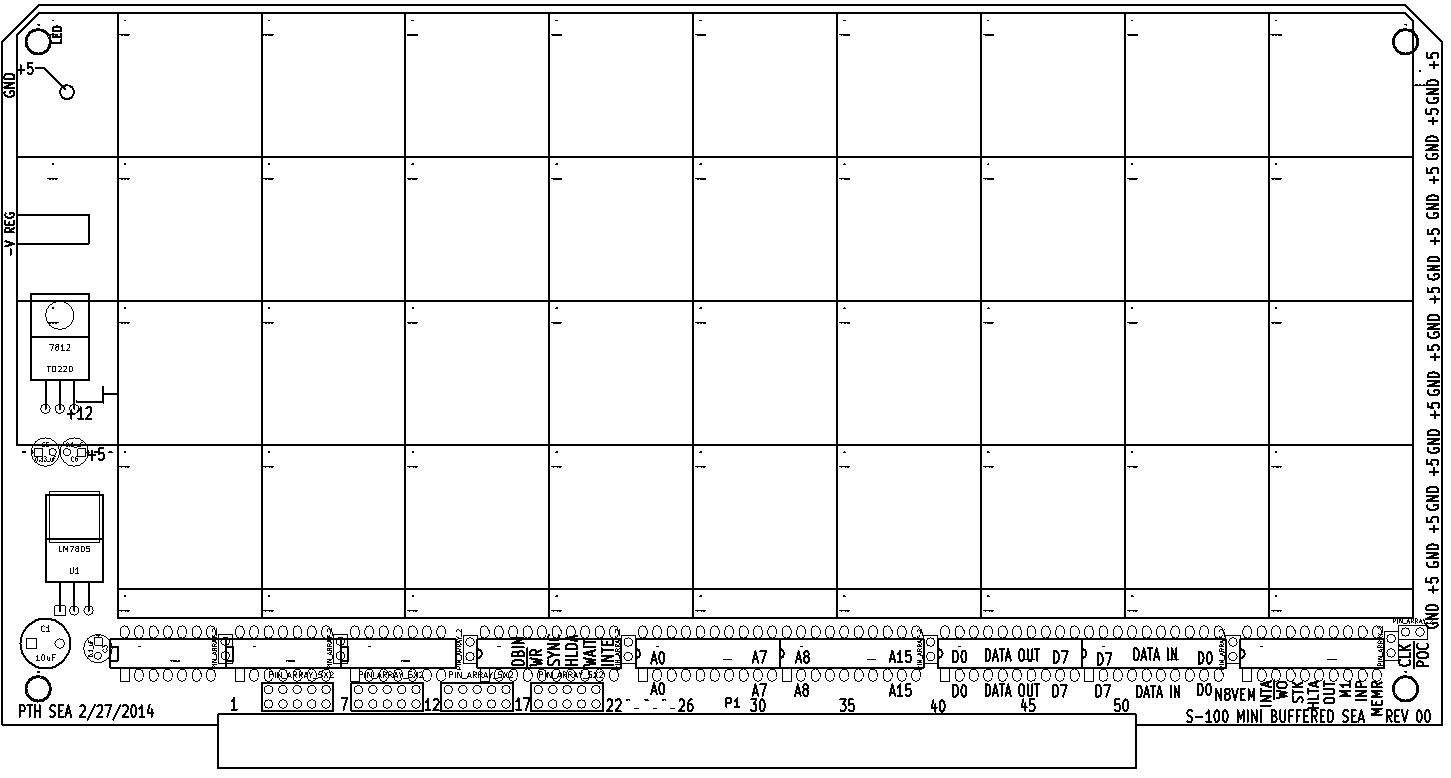
The 14 pin chips are just to not waste that space, I picked 14 because most designs use either a 7400 or 7404. I could space them a little more and remove 1 capacitor from in between. I do go over kill on the decoupling capacitors.
Date: Sat, 1 Mar 2014 02:39:50 -0500
Subject: Re: [N8VEM-S100:2589] Re: Board Run: Unbuffered Prototyping
From: pbi...@gmail.com
To: n8vem...@googlegroups.com
Thanks for the updated foils & silkscreen. What's with the three left-hand uncommitted DIP-14s and the two overlapped decoupling caps (which I guess could be attached to the underside)? Can you also share the updated schematic? How did you chose the end-point for the 5v power LED -- it seems to be "at sea" rather than "in harbor"?
On Fri, Feb 28, 2014 at 10:55 PM, Crusty OMO <crus...@hotmail.com> wrote:
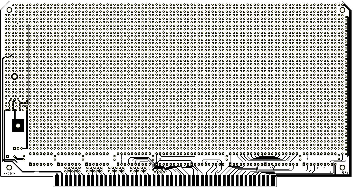
I printed a the foil patterns and got a more accurate view.
The chips on the bottom row are 6 74LS245's, from right to left, they provide
Status, Data In, Data Out, A8-15, A0-7, Control. 3 more 14 pin chips are to the left, with VCC and GND.
Holes are all down 50mil, Regulator has shifted to the right 100mil.
Original Unbuffered board gave 45 rows, this buffered board gives 42 rows.Copper:
Component
Silk - Grids are 10 by 10 holes. The 5V for the LED is marked, 5V and GND available from right.
The 7812 and 7912 Regulators are optional, if not installed, other chips can straddle the pads used.
--
You received this message because you are subscribed to the Google Groups "N8VEM-S100" group.
To unsubscribe from this group and stop receiving emails from it, send an email to n8vem-s100+...@googlegroups.com.
For more options, visit https://groups.google.com/groups/opt_out.
--
You received this message because you are subscribed to the Google Groups "N8VEM-S100" group.
To unsubscribe from this group and stop receiving emails from it, send an email to n8vem-s100+...@googlegroups.com.
For more options, visit https://groups.google.com/groups/opt_out.--
You received this message because you are subscribed to the Google Groups "N8VEM-S100" group.
To unsubscribe from this group and stop receiving emails from it, send an email to n8vem-s100+...@googlegroups.com.
For more options, visit https://groups.google.com/groups/opt_out.