Hi Paul,
Sure. I will first separate each board with paper, then wrap them in 1mm foam and seal it with shipping tape.
Then I'll wrap it up in bubble-wrap to fill the 3-1/2" of roomy cargo space inside that luxurious box.
One box will do, I saw they have a limit of 20lbs on that box (for international), so I will guess that domestic should at least offer that much, which is plenty more than enough. 8 boards only weighs about 1Kg, (2.2lbs)
Do you know if the $12 covers the cost of the box too? What a great deal! USPS gives some real nice value for the money.
Regards,
Josh Bensadon
Date: Wed, 5 Mar 2014 03:28:36 -0500
Subject: Re: [N8VEM-S100:2658] Mini buffered Prototyping board available.
From: pbi...@gmail.com
To: n8vem...@googlegroups.com
--
You received this message because you are subscribed to the Google Groups "N8VEM-S100" group.
To unsubscribe from this group and stop receiving emails from it, send an email to n8vem-s100+...@googlegroups.com.
For more options, visit https://groups.google.com/groups/opt_out.
Sure. I will first separate each board with paper, then wrap them in 1mm foam and seal it with shipping tape.
Then I'll wrap it up in bubble-wrap to fill the 3-1/2" of roomy cargo space inside that luxurious box.
One box will do, I saw they have a limit of 20lbs on that box (for international), so I will guess that domestic should at least offer that much, which is plenty more than enough. 8 boards only weighs about 1Kg, (2.2lbs)
Do you know if the $12 covers the cost of the box too? What a great deal! USPS gives some real nice value for the money.
Regards,
Josh Bensadon
Date: Wed, 5 Mar 2014 03:28:36 -0500
Subject: Re: [N8VEM-S100:2658] Mini buffered Prototyping board available.
From: pbi...@gmail.com
To: n8vem...@googlegroups.com
Looks sweet :->. I'm in for 8 (eight) with the proviso that (1) I'll wait until you do your next cross-border excursion, and (2) you use a USPS Flat Rate Medium Box (either 1 or 2) which should be really cost-effective (~$12; see: http://postcalc.usps.com/ ) and physically very safe if you put some bubble-wrap 'round them first. Please?
On Tue, Mar 4, 2014 at 7:06 PM, Crusty OMO <crus...@hotmail.com> wrote:
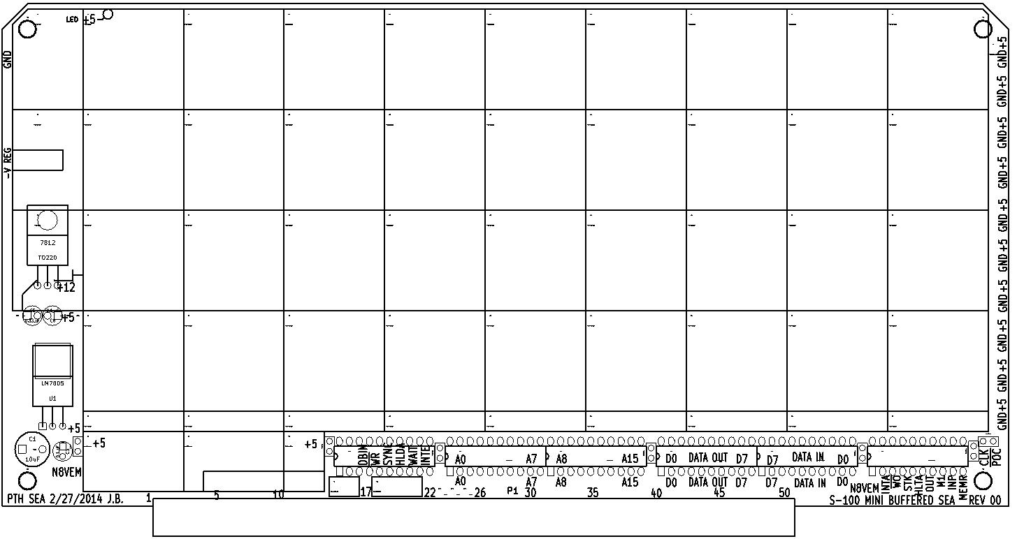
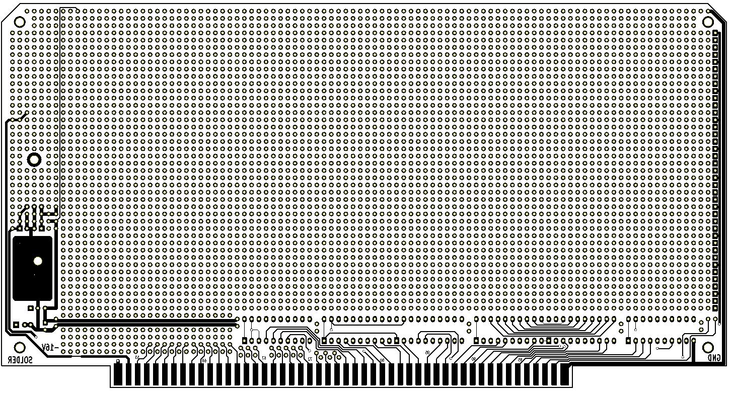
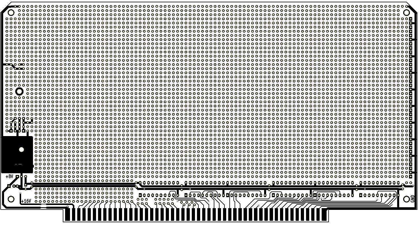
Yes, I'm going with 0.040 holes. Here's a picture of the final design. The majority of the board is for prototyping. If you don't want to use the buffer chips, you can ignore them and go for the signals available on the pins. The bottom holes outlined in the silk screen are connected to the S-100 bus, but you can easily cut traces if you want to set those holes free to the sea. There is the option to use the 12V and -12V regulators, or you can ignore those and use the pads around that area. I moved the 5V for the LED and removed the DB9.
The +8V, +/-16V traces all have fusible links, these links are rated 2Amps for 8V and 1Amp for 16V and will hopefully save the entire trace and the gold finger from damage. All chips are 74LS245. I might just add grid letters and numbers to the silk screen layer, otherwise, this is the design. There is a single pad with 5V along the top, intended for an LED with a resistor towards the ground pad to the left. Optionally, you can use this pad for VCC power, but it's only a 0.012" trace supplying power. Enough for a row of TTL. Power and ground are also available from pads on the right side. Finally, I have checked 3 times the connection between S-100 and the Buffer chips. The buffer chips are all wired for a peripheral board (Memory, I/O, etc), only the Data IN/OUT buffers must get driven with a chip enable function. If the default signals are not desired, they can be changed by breaking the small 0.008" traces which are all on the bottom of the board.
How does it look?
Date: Tue, 4 Mar 2014 09:23:23 -0500
Subject: Re: [N8VEM-S100:2640] Mini buffered Prototyping board available.
From: pbi...@gmail.com
To: n8vem...@googlegroups.comDe we get to find out the Final Clearance configuration/layout :->?On Tue, Mar 4, 2014 at 9:19 AM, Fabio Battaglia <hkzl...@gmail.com> wrote:
3 boards for me, directly from Canada is fine. How much and where should I send the money? :-)
On Mar 4, 2014 3:16 PM, "Crusty OMO" <crus...@hotmail.com> wrote:Hi,
I'm ready to go for a run of these Mini-buffered Prototyping boards.
Shipping varies. But you have 2 options. I can ship up to 5 boards in a box from Canada for $16 (flat rate small package)
or you can wait until Mid-April, I can cross the boarder and ship in strong cardboard envelopes at Andrew's rates.
I want to get some pre-orders, before making the run.
Regards,
Josh Bensadon
Date: Sun, 2 Mar 2014 09:56:43 -0500
Subject: Re: [N8VEM-S100:2601] Re: Board Run: Unbuffered Prototyping
From: pbi...@gmail.com
To: n8vem...@googlegroups.com
I very much like what you'd done with the sea-flow.
Personally, I'd never put a DBxx directly on an S100 board. Instead use an IDC-type cable with a 2xN connector and ribbon . The DBxx belongs on the bulkhead. So I'm not enthusiastic about that change.
As for the LED, perhaps a placement consistent with what's used on the 80286 master/Slave CPU Board would avoid the (potential) card ejector handle. Or maybe just scrap it and let folks wire what they want, if they want anything at all? After all, they'll probably be bringing PWR/GND "around" for ICs anyway. So let them wire-where-they-will, rather than committing to that corner? (OTOH, they can always just cut the trace ...)
On Sat, Mar 1, 2014 at 11:12 PM, Crusty OMO <crus...@hotmail.com> wrote:
Guys, Please find attached latest art work for this board.
I've done away with the 14 pin dips and let the "Sea of PTH" flow into that area.
Power runs through it.
I mixed in the terminations for S-100 bus to the lowest 2 rows of of the sea.
Look at top right, I added a DB connector, less the DB mounting holes.
I think it would be very handy to have this option, one can always put an IC over top the skewed pins if they don't want DB9. I'll keep the DB9 there unless it gets voted off the island (or sea).
It looks like it's ready to go... 2 questions still loom.
1. Position of LED,
2. Size of holes (I reduced to .038 from .042... I'm now thinking that was a mistake)
Cheers,
Josh
--
You received this message because you are subscribed to the Google Groups "N8VEM-S100" group.
To unsubscribe from this group and stop receiving emails from it, send an email to n8vem-s100+...@googlegroups.com.
For more options, visit https://groups.google.com/groups/opt_out.
--
You received this message because you are subscribed to the Google Groups "N8VEM-S100" group.
To unsubscribe from this group and stop receiving emails from it, send an email to n8vem-s100+...@googlegroups.com.
For more options, visit https://groups.google.com/groups/opt_out.
--
You received this message because you are subscribed to the Google Groups "N8VEM-S100" group.
To unsubscribe from this group and stop receiving emails from it, send an email to n8vem-s100+...@googlegroups.com.
For more options, visit https://groups.google.com/groups/opt_out.
--
You received this message because you are subscribed to the Google Groups "N8VEM-S100" group.
To unsubscribe from this group and stop receiving emails from it, send an email to n8vem-s100+...@googlegroups.com.
For more options, visit https://groups.google.com/groups/opt_out.
--
You received this message because you are subscribed to the Google Groups "N8VEM-S100" group.
To unsubscribe from this group and stop receiving emails from it, send an email to n8vem-s100+...@googlegroups.com.
For more options, visit https://groups.google.com/groups/opt_out.
--
You received this message because you are subscribed to the Google Groups "N8VEM-S100" group.
To unsubscribe from this group and stop receiving emails from it, send an email to n8vem-s100+...@googlegroups.com.
For more options, visit https://groups.google.com/groups/opt_out.
--
You received this message because you are subscribed to the Google Groups "N8VEM-S100" group.
To unsubscribe from this group and stop receiving emails from it, send an email to n8vem-s100+...@googlegroups.com.
For more options, visit https://groups.google.com/groups/opt_out.


