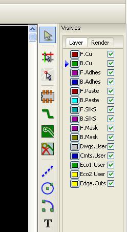
On KiCad PCB, the latest version I just recently downloaded, there's a tool bar on the right that lets you turn layers on/off. Very helpful to reduce screen clutter when doing detailed work.
Here's a screen capture of that toolbar. You can also click the colour box and change colour of that layer.
I don't know if this tool bar can be turned off/on, it was on after a default installation.

From: mon...@vitasoft.org
To: n8vem...@googlegroups.com
Subject: RE: [N8VEM-S100:3723] New run of S-100 EPROM/RAM boards...
Date: Mon, 19 May 2014 11:26:24 -0700
Ed, going to give it a try too…
On “DRC”, Is it Preferences/General Settings/”Enforce design rules when routing”
Which icon (counting from, say top) on LHS to show say just the front copper traces layer.
None of mine seem to do that. Do I need to add an icon or something?
John
From: n8vem...@googlegroups.com [mailto:n8vem...@googlegroups.com] On Behalf Of Crusty OMO
Sent: Monday, May 19, 2014 6:20 AM
To: n8vem...@googlegroups.com
Subject: RE: [N8VEM-S100:3720] New run of S-100 EPROM/RAM boards...
Hi Ed,
I just recently learned KiCad PCB layout only when I did the Sea of PTH buffered prototyping boards.
I was using just the PCB portion without creating a netlist and manually routing the traces without any error check.
Kind of like manual control. I am busy at the moment doing the 8080 board and on that project I am learning the schematic portion of KiCad (I will need all the help I can get when laying out the board).
Anyway, I learned KiCad through watching portions of an online tutorial. Running in manual is pretty easy, but first you must turn off Design Rule Check (DRC) in the preferences menu. It's there in the preference menu that you enable the various types of trace widths you want available in your design. After that, its just a matter of learning the various drawing tools. Another tip, on the right hand tool bar, you can turn off display of certain layers, also, you can turn off rendering of layers to improve speed, just turn them back on before plotting.
I think these changes can all be done in "Manual Mode", saves you from having to learn the all of KiCad.
Also, there is a feature called autopan while dragging. I turn it off because I'm not used to it, just my preference.
Good luck,
Josh
Date: Sun, 18 May 2014 18:19:32 -0700
From: zipps...@gmail.com
To: n8vem...@googlegroups.com
Subject: Re: [N8VEM-S100:3719] New run of S-100 EPROM/RAM boards...
I'm not used Kicad, other than generating gerbers (I've been using Eagle), but if no one else steps forward
I'll see if I can make some of these changes before getting these made. I guess I need to get familiar with Kicad eventually.
Ed
On Sunday, May 18, 2014 3:39:34 PM UTC-5, lynchaj wrote:
Hi Tom
Here is your chance to improve the boards. We still need a volunteer to update the S-100 RAM&ROM board and you could make the fixes and clean up the silkscreen.
Thanks and have a nice day!
Andrew Lynch
--
You received this message because you are subscribed to the Google Groups "N8VEM-S100" group.
To unsubscribe from this group and stop receiving emails from it, send an email to n8vem-s100+...@googlegroups.com.
For more options, visit https://groups.google.com/d/optout.
--
You received this message because you are subscribed to the Google Groups "N8VEM-S100" group.
To unsubscribe from this group and stop receiving emails from it, send an email to n8vem-s100+...@googlegroups.com.
For more options, visit https://groups.google.com/d/optout.
--
You received this message because you are subscribed to the Google Groups "N8VEM-S100" group.
To unsubscribe from this group and stop receiving emails from it, send an email to n8vem-s100+...@googlegroups.com.
For more options, visit https://groups.google.com/d/optout.