
| Home | S-100 Boards | History | New Boards | Software | Boards For Sale |
| Forum | Other Web Sites | News | Index |
.jpg) | |
.jpg) |
 |  |
 |
 |
 |
 |
 |
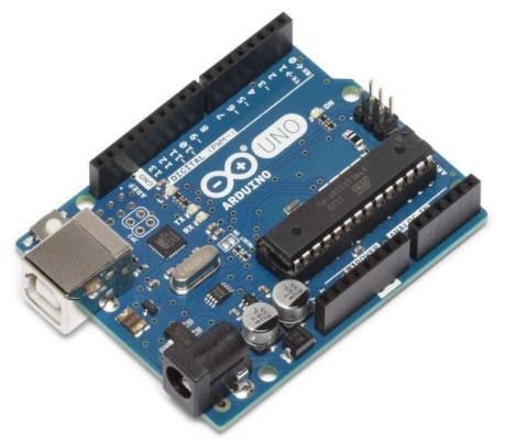
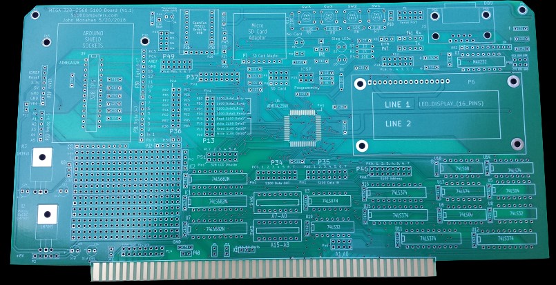
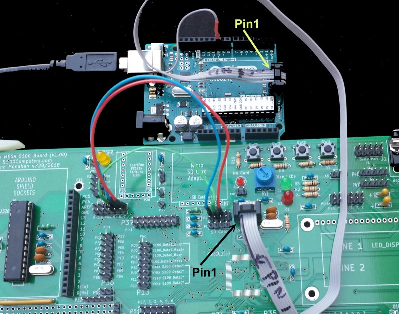
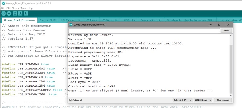
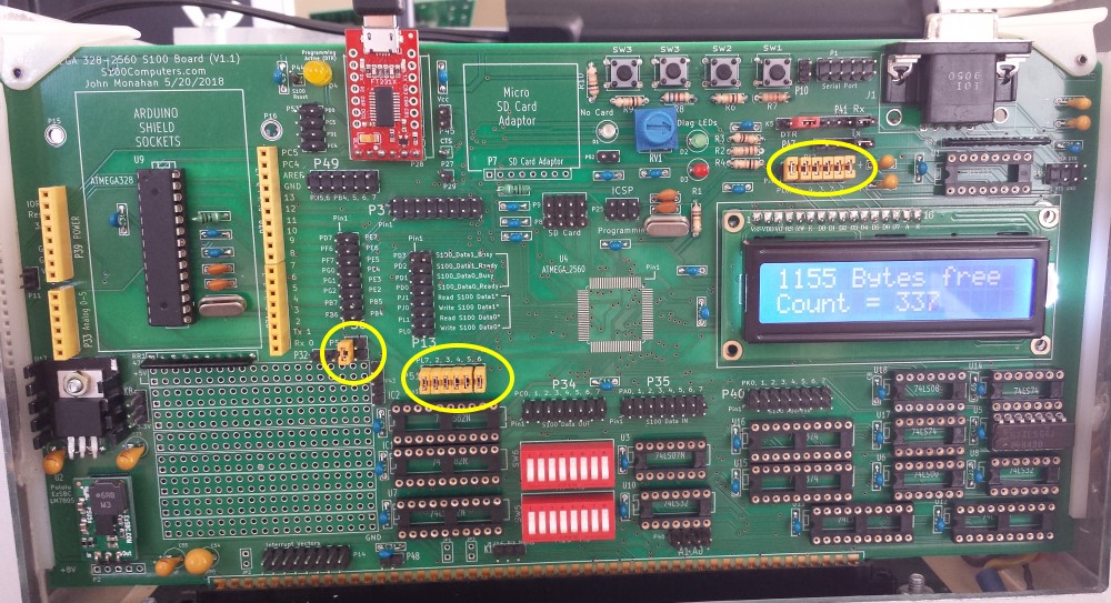
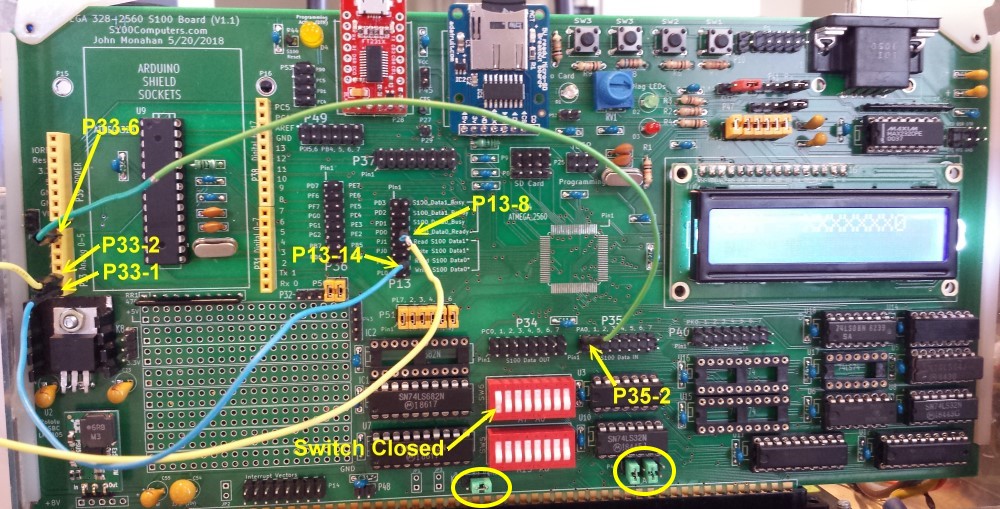
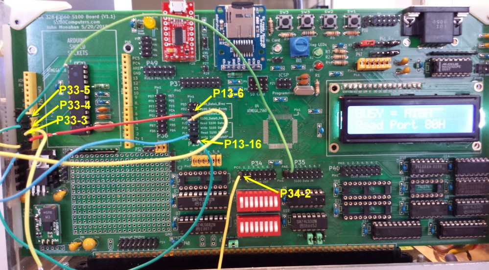
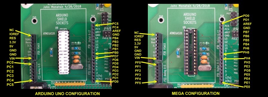
| Arduino UNO | Target | |
| D10 (SS) (P25,5) | CPU_Reset | |
| D11 (MOSI) (P9,4 <= P25,4) | MOSI (P49, 8) | |
| D12 (MISO) (P9,2 <= P25,1) | MISO (P49, 10) | |
| D13 (SCK) (P9,6 <= P25,3) | SCK (P49,12) | |
| Gnd | GND | |
| +5V | +5V |
 |
 |
 |
 |
 |
 |
 |
 |
 |
 |
 |
 |
 |
 |
 |  |
 |  |
 |
 |
 |
 |
 |
 |
 |
 |
 |
 |
 |  |
 |
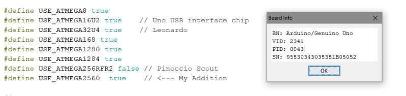
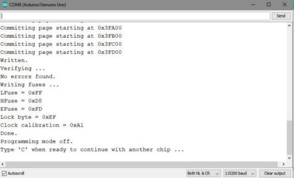
If you are up to it there is a much more sophisticated interface for the 328 & 2560 CPU chips provided free by Atmel called Atmel Studio 7. It can be downloaded here. Programming however requires you to use their Atmel-ICE Debugger. I have it but not used it. Seems like a pain to setup, Microsoft Visual C must also be resident on your PC for it to run. |
 |
| Please click
on:- DTH_DS1307.pdf MY_INFO.INO |
 |
This page was last modified on 11/17/2019