| Jumper | Function |
|
JP2 | Normally closed. Generate the S100 bus MWRT signal on this board when it is active. |
|
JP1 | Normally closed. Generate the S100 bus 2MHz Clock signal on this board when it is active. |
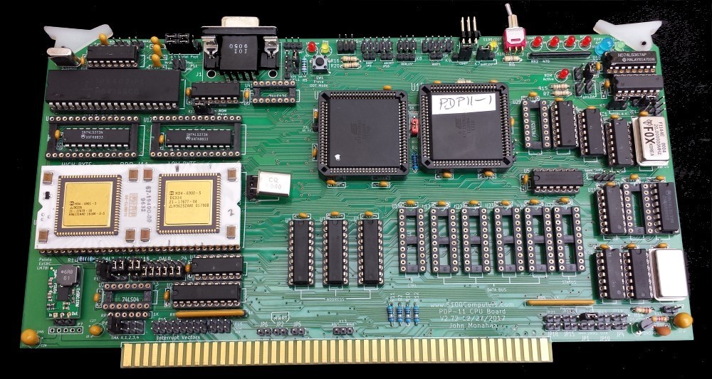
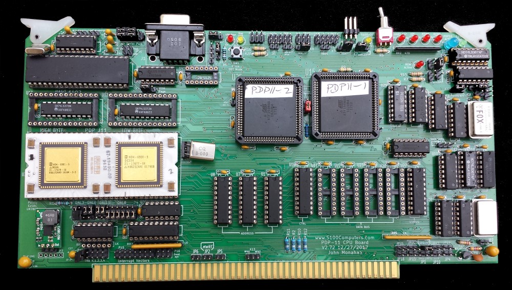
| P11 | Jumpers to accommodate RAM or ROM chips. For RAM J11 1-2. For EEPROM's leave open. |
| JP4,JP5, JP6,JP7 | Normally all open unless the board is a bus master. |
| JP13,JP15 | Normally closed to utilize the S100 bus Phantom Line.
To be safe add JP15 |
|
K2 & K8 | RAM/ROM OE* & WR* signals. For RAM jumper both 2-3. For EEPROM jumper both 1-2. |
| K1 |
Normally 2-3 |
| K9 | Normally 2-3 during board for testing/assembly. Allow S100 bus wait states with 1-2 |
| K7 | UART Select, Set 1-2 for core circuit testing. Normally 2-3 |
| K5 | For slave mode 1-2 |
| JP9 | Jumper after the
U15 CPLD is programmed |
| K6,JP12 | Set
2-3 and jumper JP12 |
| P8 | Set 1-2 and jumper JP13 |
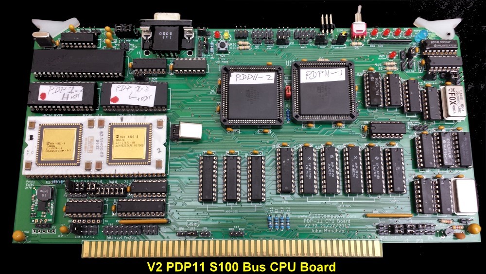
| P9 or P17 |
U15 CPLD JTAG programming socket. For Rockfield Research 1508 programmer use P9. Pin 1 is bottom left. |
|
P27 or P28 |
U25 CPLD JTAG programming socket. For Rockfield Research 1508 programmer use P27. Pin 1 is bottom left. |
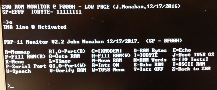
| P10 | S100 Bus TMA line to activate board. Normally 1-2 (also
jumper 3-4) . Assuming TMA0 to activate board. |
|
K4 | Currently unused. Set
aside to configure Master/Slave configurations in CPLD code |
|
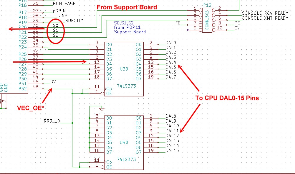
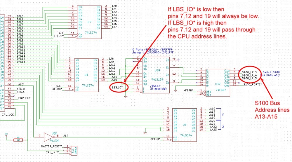
P13 | Inputs from S100 bus
Interrupt vectors. See PDP11 Support Board |
| K10/Switch | This can be a mini-switch or jumper to determine where the PDP_MON monitor data I/O is sent |
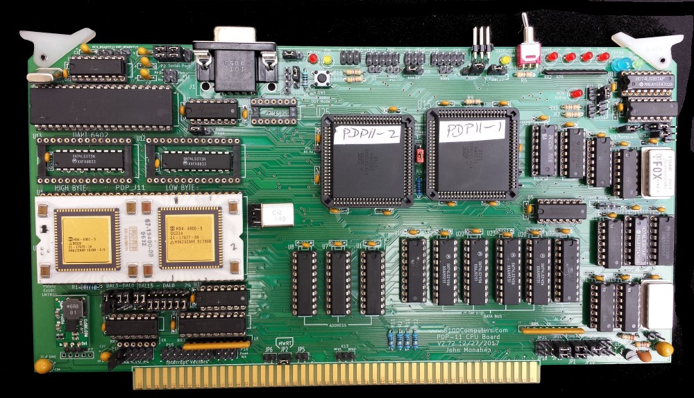
| P2 | This a serial port connector for the UART with a pinout like our Serial board. If the DB9 socket is used it must be jumpered as described above. |
|
K14 | VIP Jumper.
Used to determine if PDP11 Support Board is present. If so, jumper
1-2, if not 2-3. |
|
K12 | Used to select
Upper/Lower EEPROM. For debugging use 1-2. For page management use
2-3. |
|
P22. P25 | These jumpers
allow the onboard UART status signals to reach the P13 connector. Normally
not jumpered. |
|
K13, JP20, JP19 | Unused
jumpers to S100 bus unused bus lines. |
| SW1 |
Pushbutton
switch to force PDP11 into HALT/ODT mode. |
| K12 |
For the
High/Low ROM page option 2-3. Initially start with 1-2. |
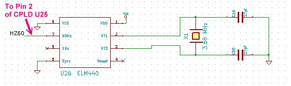
| P31 |
60Hz timer
signal from the ELM timer chip U28 |
| P12 |
Currently
unused. Can be used for configuration status bits |