S100 SCSI Interface Board
Introduction
A SCSI (Small Computer System Interface)
drive interface is a standardized way for computers to communicate with
peripheral devices such as hard disks, tape drives, CD-ROMs, and scanners.
Instead of connecting each device directly to the CPU in a unique way, SCSI
defines a common command set and electrical interface so multiple devices can
share a single bus. Each device on a SCSI chain has its own ID, and the system
can address them individually, allowing several drives (including disks and tape
units) to operate efficiently on the same connection. SCSI supports relatively
advanced features for its time, such as command queuing and the ability for
devices to communicate with each other without constant CPU involvement.
SCSI originated in the late 1970s and early
1980s, evolving from earlier proprietary interfaces like Shugart Associates
System Interface (SASI). It became formalized as a standard by ANSI in 1986 and
quickly gained popularity in workstations, servers, and high-end PCs due to its
flexibility and performance advantages over simpler interfaces like IDE. Over
time, SCSI went through multiple generations—such as SCSI-1, SCSI-2, Ultra SCSI,
and later Ultra320—each improving speed, cable length, and device capacity.
Variants like Wide SCSI increased the data path width, while differential
signaling improved reliability over longer distances, which was particularly
useful in enterprise environments.
Although traditional parallel SCSI has largely been replaced in modern systems,
its concepts live on in newer technologies. Interfaces such as Serial Attached
SCSI (SAS) continue to use the SCSI command set while switching to faster,
point-to-point serial connections. Even consumer technologies like USB mass
storage and SATA drives borrow elements of SCSI’s command structure. Today, SCSI
remains most relevant in enterprise storage—especially in servers and data
centers—where reliability, scalability, and advanced control over storage
devices are still critical.
How a SCSI chain is wired (Classic Parallel SCSI)
A traditional (parallel) SCSI setup is a
shared bus—one cable with
multiple devices attached along it. Each device (hard disk, tape drive, etc.) is
assigned a unique SCSI ID
(typically 0–7 for narrow SCSI, 0–15 for wide SCSI). The host adapter
(controller card) is also a device on the bus, often using ID 7 because it has
the highest priority. Devices can be internal (on a ribbon cable inside the PC)
or external (via a shielded cable), and both can exist on the same chain.
A critical detail is
termination: the SCSI bus must
be electrically terminated at both
physical ends of the cable—no more, no less. Terminators prevent signal
reflections that would otherwise corrupt data. Many devices have built-in
terminators that can be enabled/disabled with jumpers or switches. Only the
devices at the two ends of the chain should have termination turned on;
everything in between must have it off. Cable length and quality also
matter—faster SCSI versions required shorter, better-controlled cables.
IDE (also called PATA)
An IDE interface is much simpler but less
flexible than SCSI. Each IDE cable supports
only two devices, configured
as master and slave using
jumpers. There’s no concept of a shared multi-device bus beyond that pair, and
devices cannot independently arbitrate for control like SCSI devices can. IDE
was common in consumer PCs because it was cheaper and easier to configure.
SATA (Serial ATA) replaced IDE and simplified things even further.
Instead of sharing a cable, each drive gets its own
point-to-point connection to
the motherboard—no IDs, no termination, no master/slave settings. This makes
setup very straightforward and improves reliability and speed. However, SATA
lacks some of the advanced multi-device coordination and enterprise features
that SCSI historically provided.
The
NCR 5380 SCSI
bus controller
The
NCR
5380 SCSI bus controller is a
classic single-chip interface designed to
connect a microprocessor system (such as an
8-bit or 16-bit CPU) to a SCSI peripheral
bus. Introduced in the early 1980s, it
implements the core functions required by
the SCSI-1 standard, including bus
arbitration, selection/reselection, and
control of data transfer phases. Rather than
being a complete “smart” controller, the
5380 is often described as a
low-level or “dumb” SCSI controller,
meaning that much of the protocol handling
is managed in software by the host CPU. This
made it flexible and relatively inexpensive,
which is why it appeared in many early
workstations, expansion cards, and embedded
systems.
Technically, the 5380 provides an 8-bit
parallel data path and a set of registers
that allow the host system to directly
manipulate SCSI control signals such as REQ,
ACK, BSY, SEL, and ATN. It supports both
programmed I/O and limited DMA-style
transfers (often with the help of an
external DMA controller like the Intel
8237). Because it exposes the SCSI bus
phases quite directly, software must
actively manage handshaking and timing
during reads and writes. This results in
higher CPU overhead compared to later SCSI
chips, but also gives developers
fine-grained control—something that made the
5380 popular in custom and experimental
designs.
Historically, the 5380 became one of the
most widely used early SCSI interface chips
and helped establish SCSI as a practical
standard for connecting disks, tape drives,
and other peripherals. It was used in a
variety of systems ranging from early UNIX
workstations to add-on boards for personal
computers. Later generations of
controllers—such as the NCR 53C90 and more
advanced SCSI ASICs—integrated more
intelligence and offloaded protocol handling
from the CPU. Even so, the 5380 remains well
known among retro-computing and
embedded-systems enthusiasts for its
simplicity, transparency, and foundational
role in the evolution of SCSI technology.
Programming the NRC5380
The
NCR 5380 SCSI bus controller
supports several different
programming and data-transfer modes,
ranging from very simple
CPU-controlled transfers to
higher-speed DMA-assisted operation.
The chip itself is relatively low
level, so the host processor still
manages much of the SCSI protocol in
software, but the various modes
determine how data bytes move
between the SCSI bus and system
memory.
The simplest mode is usually called
Programmed I/O (PIO) or
polled mode. In this mode,
the CPU continuously watches the
5380 status bits to determine when
the target device is ready for
another byte. The processor reads or
writes each byte directly through
the chip’s data register while also
handling the SCSI REQ/ACK handshake.
This approach is easy to understand
and debug, which is why many early
hobbyist and embedded systems used
it, but it consumes considerable CPU
time because every transferred byte
requires software intervention.
For better performance, the 5380
also supports
interrupt-driven operation.
Instead of continuously polling the
controller, the CPU allows the chip
to generate an interrupt whenever a
SCSI event occurs—such as a phase
change or data request. This reduces
wasted CPU cycles because the
processor can perform other tasks
until the interrupt arrives. The
actual byte transfers may still be
CPU-controlled, but the system
becomes much more efficient than
pure polling mode.
The highest-performance mode
supported by the 5380 is its
DMA (Direct Memory Access) mode.
In this configuration, the
controller cooperates with an
external DMA controller—commonly an
Intel 8237 DMA chip in
8086/8088 systems—to transfer blocks
of data directly between memory and
the SCSI device with minimal CPU
involvement. The 5380 provides
special DMA handshake signals and
internal logic to automate the SCSI
REQ/ACK timing during transfers.
Once initialized, the DMA controller
moves bytes automatically while the
5380 handles the bus handshaking.
This dramatically improves
throughput and reduces processor
overhead, especially during large
disk or tape transfers. However,
implementing DMA is more complex
because both the DMA controller and
the SCSI chip must be synchronized
correctly.
Another important operating concept
in the 5380 is its support for
different
SCSI bus phases. Regardless
of whether PIO or DMA is used,
software must manage transitions
between phases such as Command, Data
In, Data Out, Status, and Message
phases. The chip exposes these
phases through status registers,
allowing software to determine what
type of transfer is currently
occurring. Because the 5380 leaves
much of the protocol sequencing to
software, programmers have very
direct visibility into how the SCSI
bus operates internally, which is
one reason the chip became popular
in educational and experimental
systems.
For this board we will design the
circuit that allows the DMA mode.
However most systems will not
utilize the full DMA capability
using a DMA controller etc.
The
SCSI Board Circuitry
The complete schematic of the prototype board can be seen
here.
The board circuit can be split into its "normal" address/data
line components and its S-100 status and control signals. The NRC5380
in "DMA" mode however requires that its internal I/O port address (A0,A1 and
A2) are setup
before any data
transfers take
place in DMA mode. This is done by latching
the A0, A1 and A2 address lines into a 74LS374. Then the normal data/status
transfer of information takes place. In "normal" IO mode the address lines
can be connected directly to the NRC5380 chip.
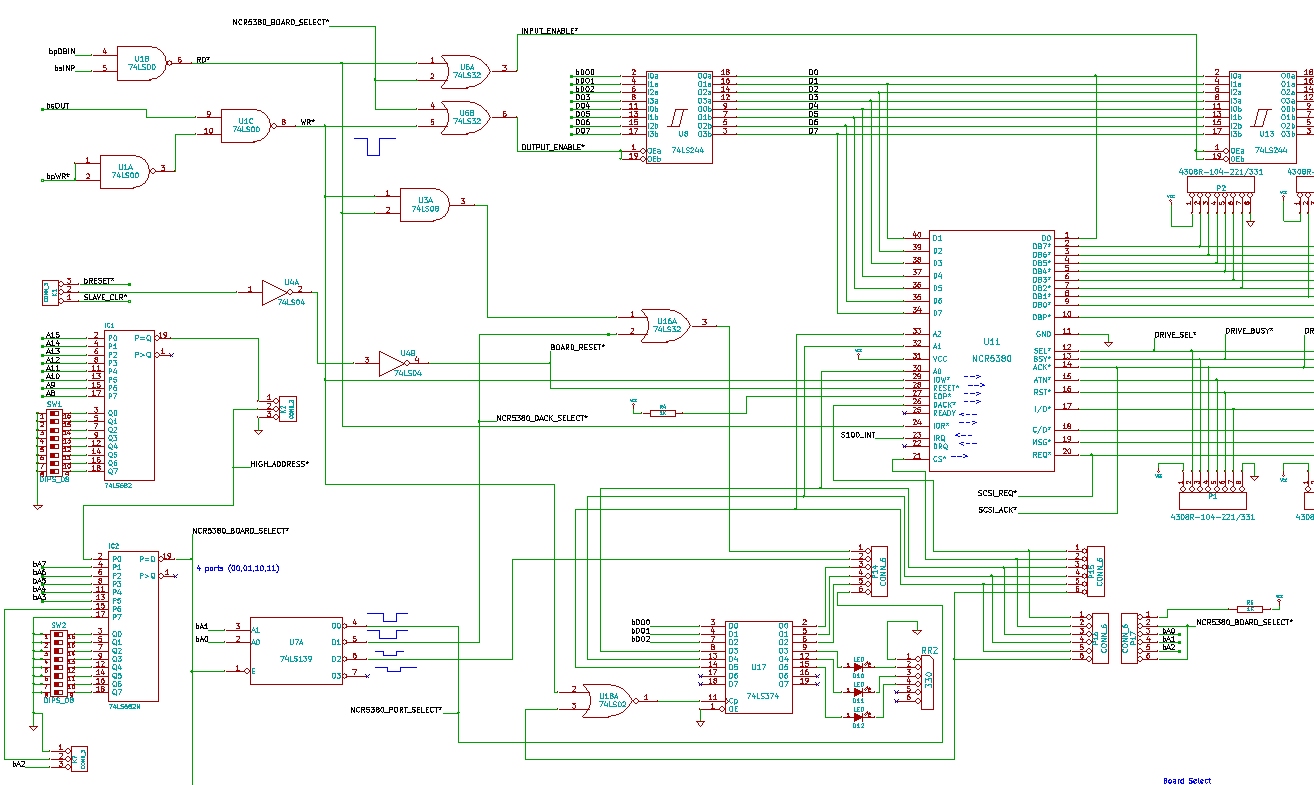
The jumpers
P14 to P15 and
K3 2-3 allow DMA mode, while
P16 to P17 and
K3 1-2 allows simple IO
mode.
The actual data to/from
the NRC2380 chip goes over the internal bidirectional data bus on the board.
This is the approach we have used on a number of our S100 Computers boards
and works very reliably. The actual ribbon cable connection to the drive
should be good quality and incorporates pull-up/pull-down resistors on the
board as in most SCSI drive circuits. There are numerous LED's on the board
which are useful mainly initially for debugging when the various ports are
tested in software loops.
Building the SCSI Board
This board is one of our simplest boards to build. The
only specialized parts (beside the NCR 5380 chip) are the four pull-up-pull
down resistor networks for the SCSI connecting cable. These are
necessary even for a short SCSI cable. They are
220 Ohm/330 Ohm Network
arrays, quite common. The Mouser part # is
652-4308R104221/331L I used seems to
have slightly different values but definely work fine.
The first step is to examine the
bare board carefully for scratches or damaged traces. Use a magnifying glass
if need be. The quality of the boards we get is excellent. I must have done
hundreds by now, never had a problem, but there is always a first time. A
broken trace is almost impossible to detect by eye on a completed board.
Next solder in all the required IC sockets, resistors, resistor arrays,
capacitors, jumpers, and the DIP switches and LED's. Be sure you put the
resistor arrays in with the correct orientation of pin 1. Check their value
before soldering (they are difficult to remove). You can use cheaper
"double swipe" IC sockets. However for a critical board like this I prefer
to use "Machine Tooled" IC sockets (e.g. Jameco # 38623). Unfortunately
they are more expensive and you have to be particularly careful not to bend
the IC pins. Typically the longer pin of a cap or LED goes into the square
pad on the board.
The Board Power Supply.
This board only requires a
single 5V supply for the circuits. There are a number of 5V regulator
options. You need to pick one.
These days there are a number of different Pololu 5V switching regulators.
They can be found
here.
The board requires less than 1 Amp at 5V. So you need to match the
pinouts of P5 or
P6 with the Pololu regulator you use.
Alternatively you can use the right three pads of
P5 with a
EzSBC 5V regulator. Recently
Pololu has come out with a cheaper 1 Amp 5V regulator (APM81815)
which works fine with this board in P5.
Before adding any IC chips put the board in the bus and check all the IC
sockets are receiving a 5 volt supply.
Testing Software
Before jumping in and writing a sophisticated CPM3 BIOS for this board its
best to start off with a simple software program to just read and write a
defined sector on to a SCSI drive. We will assume here that our SCSI drives
ID is 1 and the Base IO port for the controller chip is
48H.
This can be reconfigured easily in the program (see below), but a continuous
block of 8 ports is required starting an any 8 byte port boundary.
The coding is fairly straightforward except as explained above for each IO
port access to the NRC5380 that port must be latched into U17 if the DMA mode
is used. For simple testing we will use the simple IO mode and the
program
SCSITEST. Z80.
This program can be downloaded at the bottom of this page.
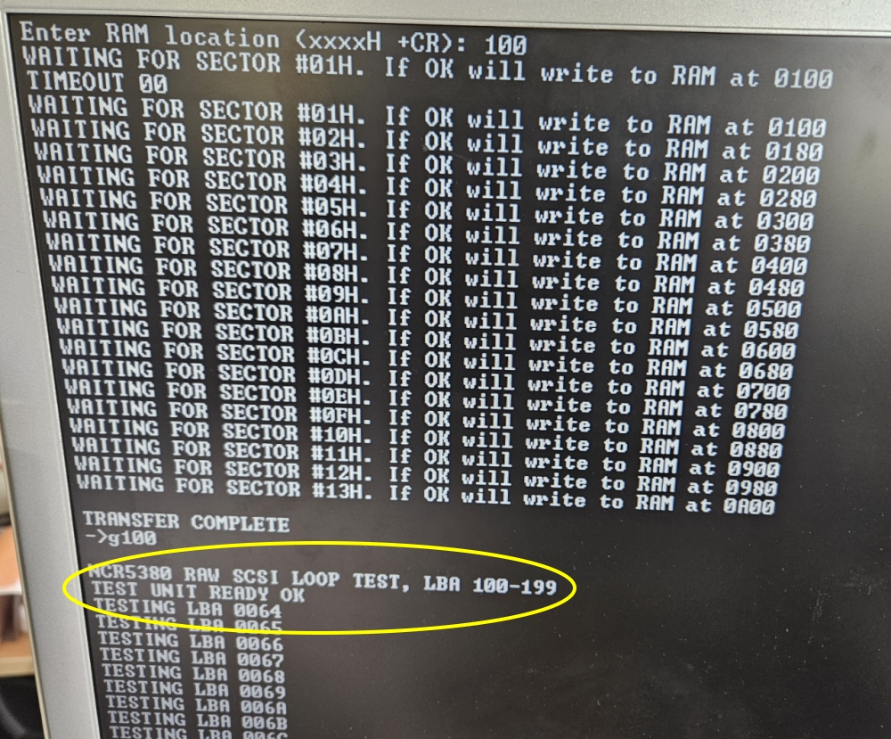
Do not waste time going further until you get the above program to work.
Remember there are two modes the
NCR5380
board works in.
Here we will work with the simplest mode the "Ports IO Mode". In this
mode all the jumpers of
P14
are connected to
P15.
There are no jumpers for
P16
and
P17.
I have tested this board
with a
Seagate "Hawk" ST31230N
drive and a
Seagate "Barracuda"
ST34371N drive.
I have not played around much using the board in "DMA" mode. For this
mode Jumpers P16 and
P17 are connected and P14 and
P15 are open.
The relevant test program similar to the above
SCSITEST.Z80 is SCSI_DMA.Z80 also
downloadable at the bottom of this page.
I have found one quirk with the program as is (at least with these two
drives). The first time the drive is booted the program hangs. Resetting the
computer are re-running the program it runs fine, always, ever with further
reboots. I have not noticed much difference in speed with both IO and
DMA versions. BTW both are not optimized and were just basic Chat GPT
programs.
Remember both test programs are run at 100H
in RAM, assume a
Propeller Console IO and are loaded using the
Z80 MASTER monitor
"X'" command.
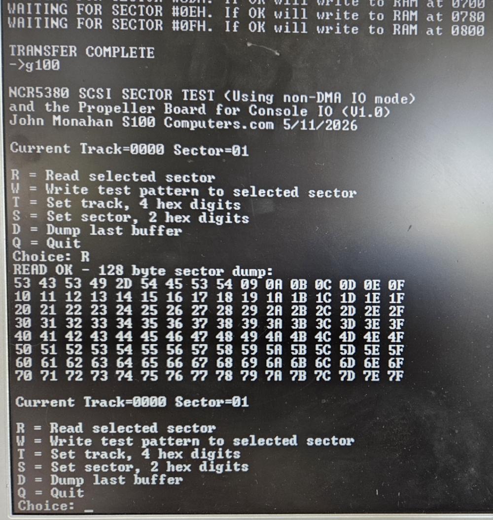
Next we will utilize a program to read and write SCSI drive sectors using
8080 code suitable to splice into a CPM3 BIOS. This program
(downloadable at the bottom of this page) is
SCSI_RW.ASM.
Again load it at 100H in RAM. Here is a
typical output.
This program must run without errors before going further.
Installing CPM3 SCSI BIOS Software
If you get this far you are well prepared to install CPM3. We will use
the CPM3 Drive BIOS file HIDE3.ASM as a
starting point where Drives A: and B: are IDE/CF Drive SD cards, We will add
a third drive a SCSI Drive C: The starting file is from
CPM3 CF Card Image #4 contained
here. This new file (generated
by
Chat GPT), named IDE3SCSI.ASM has
the following CPM3 Drive table:-
; EXTENDED DISK
PARAMETER HEADER FOR DRIVE 0:
DW HDWRT
;HARD DISK WRITE ROUTINE
DW HDRD
;HARD DISK READ ROUTINE
DW HDLOGIN$0 ;HARD DISK
LOGIN PROCEDURE
DW HDINIT$0
;HARD DISK DRIVE INITIALIZATION ROUTINE
DB 0
;RELATIVE DRIVE 0 ON THIS CONTROLLER
DB 0
;MEDIA TYPE, HI BIT SET, DRIVE NEEDS RECALIBRATING
DPH0: DPH 0,IDEHD$DPB,0
DB 0
;Drive A: Hardware Select, (IX offset 25)
; EXTENDED DISK PARAMETER HEADER FOR DRIVE 1:
DW HDWRT
;HARD DISK WRITE ROUTINE
DW HDRD
;HARD DISK READ ROUTINE
DW HDLOGIN$1
;HARD DISK LOGIN PROCEDURE
DW HDINIT$1
;HARD DISK DRIVE INITIALIZATION ROUTINE
DB 0
;RELATIVE DRIVE 0 ON THIS CONTROLLER
DB 0
;MEDIA TYPE, HI BIT SET, DRIVE NEEDS RECALIBRATING
DPH1: DPH 0,IDEHD$DPB,0
DB 1
;Drive B: Hardware Select, (IX offset 25)
; EXTENDED DISK PARAMETER HEADER FOR DRIVE 2, NCR5380 SCSI DRIVE C:
DW
SCSI$WRT
;SCSI HARD DISK WRITE ROUTINE
DW
SCSI$RD
;SCSI HARD DISK READ ROUTINE
DW
SCSI$LOGIN ;SCSI HARD
DISK LOGIN PROCEDURE
DW
SCSI$INIT
;SCSI HARD DISK DRIVE INITIALIZATION ROUTINE
DB 0
;RELATIVE DRIVE 0 ON THIS CONTROLLER
DB 0
;MEDIA TYPE, HI BIT SET, DRIVE NEEDS RECALIBRATING
DPH2: DPH 0,SCSI$DPB,0
DB SCSI$DRIVE
;Drive C: Hardware Select, (IX offset 25)
IDEHD$DPB:
DPB 512,61,256,2048,1024,1,8000H
SCSI$DPB:
DPB
512,64,256,2048,1024,1,8000H
The CF card image (#20) can be found
here. Simply load the CF card into your slot A: of your
IDE/CF Dual CF Card Board
and boot CPM3 with the monitor "P" command.
The folder to construct this image #20 can be found
here.
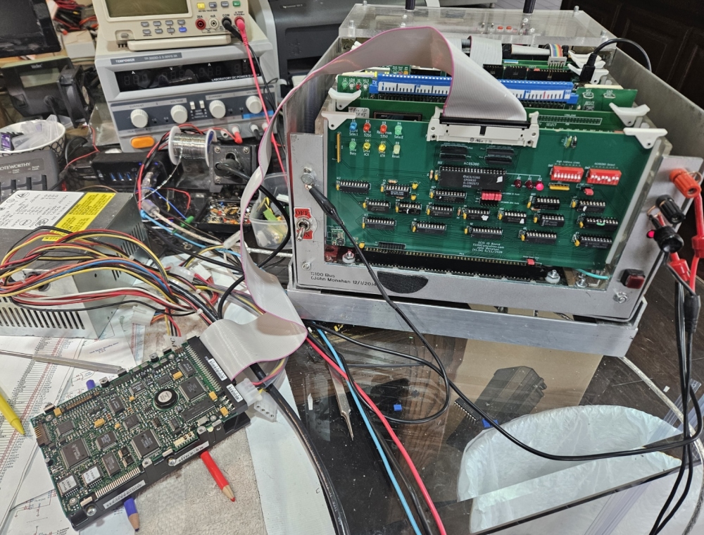
Here is what the experimental hardware looks like:-
Note this is a simple Non-Banked CPM3 disk setup. The BIOS can be
easily modified to a more useful Banked CPM3 system -- see the examples
here.
The NCR 5830 Chip.
NCR later introduced a CMOS version of the above NMOS 5380. They called it
the 53C80, but it was a 48 pin DIP that of course had a different pinout and
several other enhancements. NCR later produced a chip called the 53C80-40,
which was a drop-in replacement for the above original 5380. Subsequently
other manufacturers including AMD and Zilog have also produced a 40 pin DIP
53C80, all are compatible replacements for the original 5380. (Thanks to
Peter Higgins for this info).
To Order a Production S-100 Board
Realizing that a number of people might want to utilize a
board like this together with a group of
people on the
Google
Groups S100Computers Forum, a "group purchases" is now CLOSED.
Please see here
for more information. Please do not contact me directly.
The links below will contain the most recent schematic of the above boards.
Note, it may change over time and some IC part or pin numbers may not correlate
exactly with the text in the article above.
SCSI Board Schematic (V1.2) FINAL .PDF File (5/28/2026)
KiCAD files for
SCSI Board
(V1.2) FINAL .ZIP File 5/28/2026)
Gerber files for
SCSI Board (V1.2) FINAL .ZIP File (5/28/2026)
SCSI Board BOM .CSV File (5/27/2026)
SCSITEST.Z80
Text File (5/27/2026)
SCSITEST.ZIP
Zip File of folder (5/27/2026)
SCSI_DMA.Z80 Text File (5/27/2026)
SCSI_DMA.ZIP Zip File
of folder (5/27/2026)
SCSI_RW.ASM Text File (5/27/2026)
IDE3SCSI.ASM
Text File (5/27/2026)
Other pages describing my S-100
hardware and software.
Please click
here
to continue...
This page was last modified on
08/13/2026

.jpg)