
| Home | S-100 Boards | History | New Boards | Software | Boards For Sale |
| Forum | Other Web Sites | News | Index |
New S-100 Boards
This section of this web site lists of many of the new S-100 boards I and others have recently constructed. Still utilizing the basic IEEE-696 S100 bus format, we are incorporating modern designs into these new S100 bus boards. The long term goal being to adapt most major microprocessor chips (and support IC''s) to the S-100 bus . We have for example S-100 boards with master and slave CPU's like the 8086, 80286, 80386, 80486 family, the 68000/68030 Motorola family, the PDP11, all the way up to more recent CPU's like the Edison SoC. This has been, and will continue to be, a multi-year project. A core of enthusiastic people have got together to do this.
Index Table Of New S-100 Boards Described On This Web Site .
New S100 Computers Boards
When a new board is announced at https://groups.google.com/g/s100computers you can get one by filling in this e-mail "order form" below.
New boards typicall take 3-4 weeks to arrive. Payment for boards is via PayPal after you recieve your board(s).
The price will be announced in the Google Groups posting for each board.
This form is to be used only for new boards . For old.boards see below.
Please take care to enter your exact name and shipping address.
Shipping Status of Recent New S100 Computers Boards
The Following People are due to be shipped the 12 Slot S100 Bus Motherboard :-
| Name | Motherboard Board |
| Steven Osborne | 1 |
| Tony Gerbic | 1 |
| John Reeves | 1 |
| Terry Fox | 1 |
| Juliean Galak | 1 |
| Henry Broekhuyse | 2 |
| Todd Houg | 1 |
| Mark Huffstutter | 1 |
The Following People were shipped either or both the Z80 V3 CPU Board or Front Panel Board:-
| Name | Z80 V3 CPU Board | Front Panel Board |
| Eric Dittman | 2 | |
| Steven Osborne | 1 | 1 |
| Joe Meyer | 2 | 1 |
| Terry Fox | 2 | 1 |
| Mark Huffstutter | 2 | |
| Dominique Le Bel | 2 | 1 |
| Robert Greenstreet | 1 | |
| Jacobus de Waal | 2 | |
| William Stillwell | 1 | 1 |
| Greg Beat | 1 | |
| William Stillwell | 2 | 1 |
| Thomas L. Von Der Haar | 1 | 1 |
| Bob Grabau | 2 | |
| Randy Eubanks | 1 | 1 |
| Roy Bragg | 1 | 1 |
| Henry Broekhuyse | 2 | |
| Michael Petry | 2 | 1 |
| Michael Wachur | 1 | |
| Jay Cotton | 1 | |
| William Stewart | 1 | |
| Tim Geuy | 1 | |
| Rich Camarda | 1 | |
| William Stewart | 1 | |
| John Reeves | 2 | 1 |
| Kenny Maytum | 1 | |
| Tony Gerbic | 1 | |
| JERRY PRUSA | 2 | |
| Tim Acker | 1 | |
| Steven Hamilton | 1 | 1 |
| Krister Wenstrom | 1 | |
| Bill Lewis | 1 | |
| Peter Plank | 1 | |
| Wayne Warthen | 2 | |
| Fredric Brown | 1 | 1 |
| Charles Hicks | 1 | 1 |
| Robert Weatherford | 1 | 1 |
| Kenneth Ames | 1 | 1 |
| Greg Bober | 1 | 1 |
| Jefferey Wilson | 1 | |
| Paul Birkel | 1 | 1 + FPGA VGA |
The Following People have been shipped the SCSI S100 Board:-
| Name | SCSI Board |
| Mark Huffstutter | 2 |
| Tony Gerbic | 1 |
| John Luke | 2 |
| Bob Grabau | 2 |
| Dave McGuire | 2 |
| Roy Bragg | 2 |
| Steven Osborne | 1 |
| Keith Refior | 1 |
| Thomas Von Der Haar | 2 |
| John P. Mitchell | 1 |
| Jay Jaeger | 2 |
| mike noel | 2 |
| Jonathan Haddox | 2 |
| John Reeves | 2 |
| Henry Broekhuyse | 2 |
| Rick Bromagem | 2 |
| Martin Crockett | 1 |
| Pete Plank | 1 |
| Alex Swedenburg | 1 |
| Rich Cini | 2 |
| Andrew Pullin | 1 |
| Greg Bober | 1 |
| Terry Fox | 1 |
| Veron Sawers | 1 |
| Steven Hamilton | 1 |
Reorder Of Past S100Computers Boards
I must stress however this is a hobby based group of people (spread actually around the world these days). There is no central organization or person “in charge”. I and a few others design and produce new S100 boards (at our own expense) and when done, typically do a “group purchase” of a new board. These are bare boards which must then be stocked with chips etc. Typically I provide basic build/testing instructions and if needed, basic software.
It is unfortunately a bit difficult for new people to get started since many by now already have their basic starting boards.
The required board fabrication Gerber files are available at the bottom of each board’s description on this site if you wish to have somebody do a board for you or others.
New boards and discussions about them are always announced here:-
| https://groups.google.com/forum/?fromgroups#!forum/s100computers |
Ordering Older Boards
Todd Goodman maintain a stock of some of our most popular boards. They are listed here (along with a number of other "ReteroBrew Computer" boards).
Please see here:-
https://wiki.bonedaddy.net/doku.php?id=boardinventory for a list of boards available.
Alternatively you can get started quickly by scanning eBay for S100 bus motherboards, computer systems or S100 bus boards themselves.
Here is a good place to start:-
To help new users here are some suggested S100 Bus setups:-
Beginner :
Z80 SBC or the Z180 SBC
Starter Z80/CPM system:
Z80 CPU Board + Console IO Board + Duel IDE/CF Board + 16MB RAM + SMB
Starter Z80/CPM system II:
V3 Z80 80 CPU Board + Console IO Board + Duel IDE/CF Board + 16MB RAM
Better Z80/CPM system:-
Add ZFDC Board + Serial IO board
Basic 8086/MSDOS system:
Add 8086 Board + MSDOS Support board
Better MSDOS system:
Add Baby 80486 + VGA (16 bit) Board .
Sophisticated MSDOS system:
Add Full Size 80486 + OTT 32/64 MB RAM
Other popular boards:
68030K CPU Board , Dazzler II Board , RAM+ROM Board , Parallel Ports Board , PIC/RTC Board , 80286 , 80386 .
Note to Beginners.
Please note that building an S100 Bus computer system using these boards is not for beginners in electronics. While the build instructions for each board may look simple, getting them to run correctly is an S100 Bus computer setup is difficult for anybody with little electronics experience. Because of the time required to build and test new boards I will have no time to help you debug your board/setup. Please keep this in mind if you order a board. For beginners I highly recommend they start with something like a Arduino, Propeller or Raspberry computer system. Also, please keep in mind many of the S100Computers boards require a ROM/GAL programmer . Most of the newer more complex boards also require a CPLD programmer or a FPGA programmer as well.
Remember this is a true hobby/non-profit operation! Support is limited.
MY OWN S-100 SYSTEM
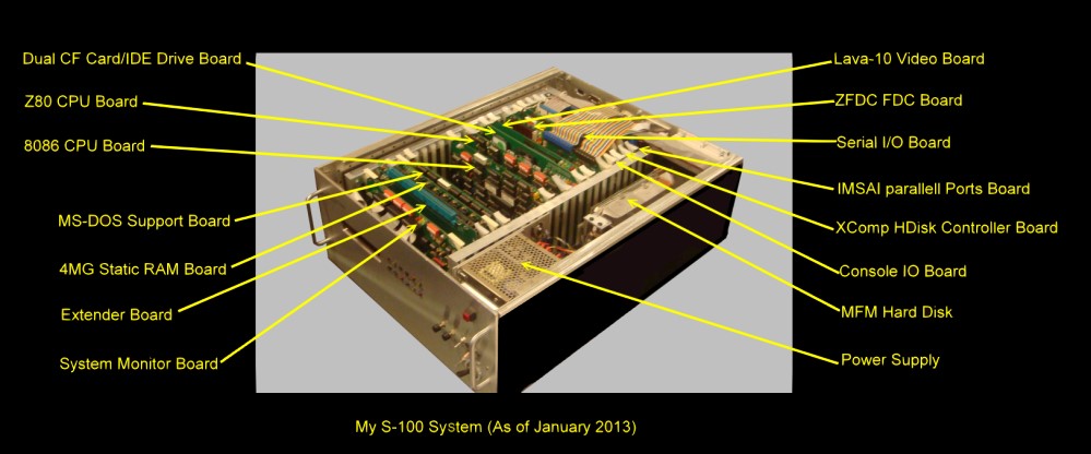
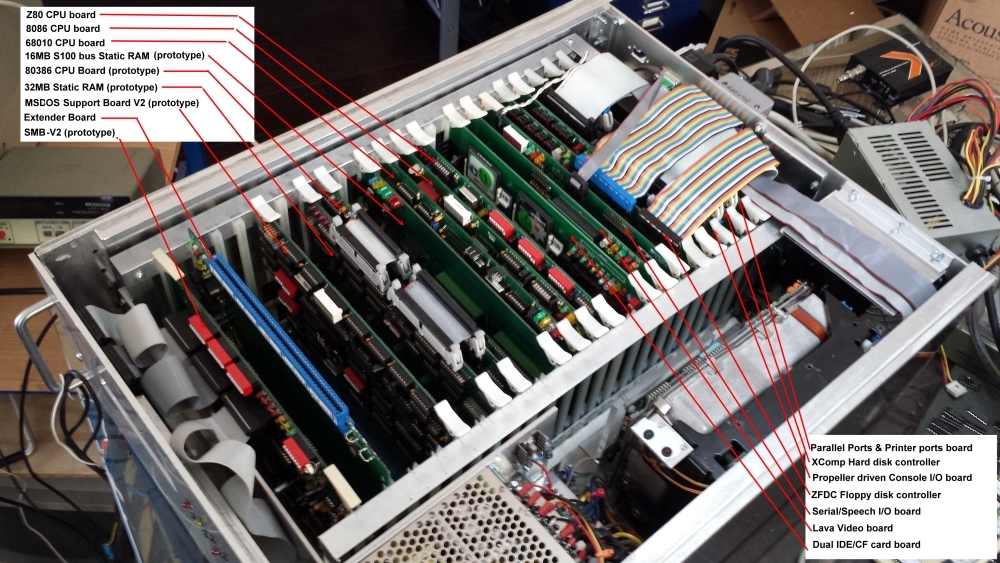
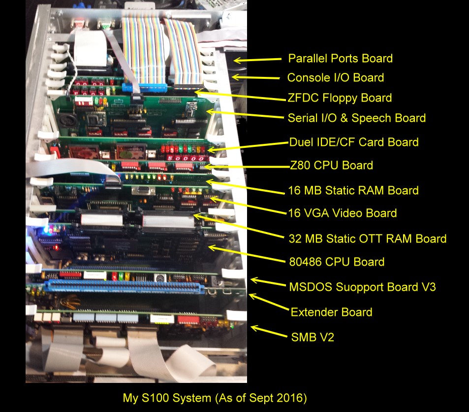
By way of showing the evolution of these boards, I will describe my own S-100 IEEE-969 system. This is a completely "homebrew system". Originally built in the early 1980's utilizing many of the S-100 boards of that era. As I add new S-100 boards, I will go into some detail in an effort to help others build similar systems or allow them revive S-100 systems they may have stored away or have recently acquired. While none of this is rocket science , it does require some degree of electronic knowledge, familiarity with the S-100 bus and for the software, a working knowledge of CP/M, CP/M86 and MS-DOS (Programs, BIOS & Drivers) . If you wish to become more informed about the S-100 bus itself try and get your hands of the book " Interfacing to the S-100/IEEE696 Microprocessors " by Sol Libes & Mark Garetz. This book is commonly regarded as the "bible" for this field. This will be a long term "work in progress" report. The index table above will direct you to new S-100 boards built or being tested. See each boards section for more details.
Readers such as yourself are encouraged to participate by joining the S100Computers Google Groups forum .
Here was my starting point for a S-100 system built with boards from the 80's. With this as a basis over time, we will swap out many of these boards into new more exciting and efficient boards using more modern IC's.
MY SYSTEM IN 2009
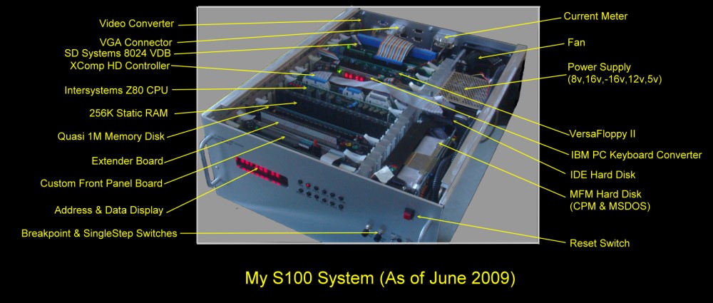
MY SYSTEM 2011

MY SYSTEM 2013
MY SYSTEM 2014
|
|
| My S-100 System (As of April 2014) |
MY SYSTEM 2016
|
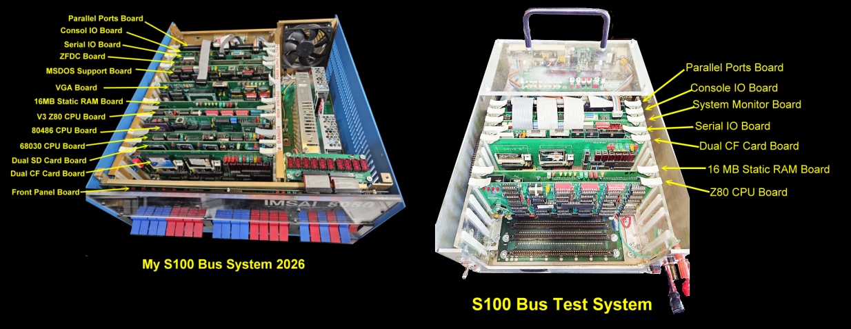
MY SYSTEM 2026
At this stage I have made over 80 S100 Bus boards. I have a number of S100 Bus Boxes with various configurations. However for each board I describe and "put out" I always test them in a 20 slot and 9 slot active terminated S100 Bus system. My current systems below consist of Robert Weatherford's Parastream IMSAI box with its own new linear power supply and a Morrow 9 Slot "Test System". I use my own custom S100 computers Front Panel in the IMSAI box.
|
Getting Started in KiCAD .
All our boards are designed using KiCAD . This is an open-source software tool for the creation of electronic schematic diagrams and PCB artwork. This is a fairly complex program to learn and will typically need weeks of practice to build up a board. After the board circuit is generated with KiCAD it must then have all the chips arranged on the board and connected with 100's if not over a 1000 traces and vias. This is done with another program called Freerouter . Finally the resulting Freerouter files must be converted to Gerber files for the factory to actually fabricated the board. For most of our boards I provide the most recent Gerber & Drill files to have a board fabricated. You may use these files -- at your own risk -- to have any board on this site made for non-commercial use.
KiCAD .
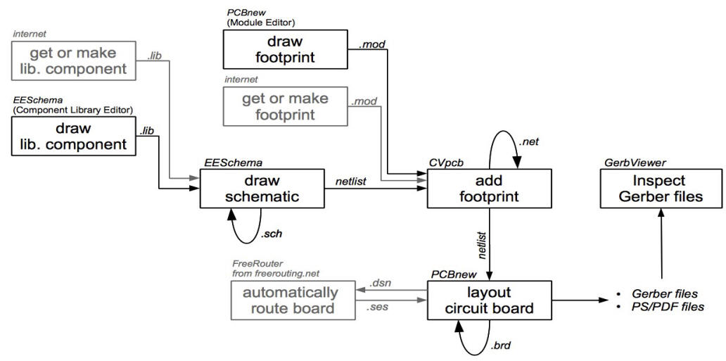
KiCAD is an open-source software tool for the creation of electronic schematic diagrams and PCB artwork. Beneath its singular surface, KiCAD incorporates an elegant ensemble of the following standalone software tools:-
KiCAD project manager
EESchema schematic editor
CVpcb footprint selector
PCBnew circuit board layout editor
GerbView Gerber viewer
Bitmap2Component component maker
KiCAD can be considered mature enough to be used for the successful development and maintenance of complex electronic boards. KiCAD does not present any board-size limitation and it can easily handle up to 16 copper layers and up to 12 technical layers. KiCAD can create all the files necessary for building printed boards, Gerber files for photo-plotters, drilling files, component location files and a lot more.
Despite its similarities with other PCB software tools, KiCAD is characterized by an interesting work-flow in which schematic components and footprints are actually two separate entities. This is often the subject of discussion on Internet forums.
The KiCAD work-flow is comprised of two main tasks: making the schematic and laying out the board. Both a components library and a footprints library are necessary for these two tasks. KiCAD has plenty of both. Just in case that is not enough, KiCAD also has the tools necessary to make new ones.
|
The main KiCAD web site can be seen here . From there you can obtain excellent instructions, videos and examples as to how to lay out printed circuit boards. However be aware to layout complex printed circuit boards like we have here needs many hours of experience and should not be taken on lightly.
To get started please review the following files:-
Getting_Started_in_KiCad.pdf
cvpcb.pdf
eeschema.pdf
KiCad.pdf
pcbnew.pdf
gerbview.pdf
Please note, in Dec 2015 a newer version of KiCAD has been placed in the public domain. Unfortunately some of the files for the previous version of KiCAD (the above 2013 version) are no longer compatible with this newer version. They can be converted, but for now I will stick with the 2013 format. All our current files should work with that version. The 2013 KiCAD version is way more than adequate for all our needs.
|
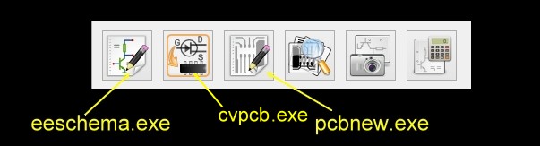
Initially you use the eeschema button to draw your schematic. This is by far the most time consuming and hardest part of the program. As I said above it takes many long hours to master this part. You then need to convert this schematic to an actual board layout with all the IC's etc. physically in place.
From your schematic you make a .net file
You then call in the second program cvpcb that uses the .net file to assign each IC in your schematic an actual board "footprint". Most common footprints are already available as .mod files that come with the many KICAD "libraries&qu
This page was last modified on 09/27/2026 September 11, 2026