I wanted thermal relief around IC pins, but not around the regulator, so I tried 2 seperate zones, but it wouldn't let me specifiy this attribute per zone. No worries, I'm not afraid of a little manual tracing. I just stuffed a thick trace around the thermal relief of the regulator TAB, problem solved. While looking things over, I decided to add another resistor in case the IO jumper is not installed. Fortunately, it was not the resistor that broke the camels back.
Anyway, I took some more time to polish off the board with more silk screen labels and indeed move some away from the via's (thought I caught them all already, but apparently not). I'm guessing if I keep looking at it, there will be other changes, but it's time to put the pencil down.
Cheers for your help!
Regards,
Josh
From: mal...@avitech.com.au
To: n8vem...@googlegroups.com
Subject: FW: [N8VEM-S100:4001] ALTAIR/IMSAI 8080 CPU replacement board
Date: Sat, 7 Jun 2014 09:51:31 +1000
Hi Josh,
I’ve solved the “fill” issue around the regulator. I deleted the heat-sink traces on both sides of the PCB, then placed “Zones” on each side of the PCB. “Zones” are “fills” in Pcbnew-speak. I will email the updated BRD file to you separately, as it is over 1MB.
To create a zone, the basic steps are as follows:
1. Select Place -> Zone from the Pcbnew menu.
2. A cross-cursor will appear. Click somewhere on the PCB (this will be the first corner of your new Zone).
3. A “Copper Zone Properties” dialog box will open. Select the “Layer” that the Zone will be on. Select the Net that the Zone will connect to. For the two Zones I created on your board, I selected “GND1” as the Net. Adjust the other “Settings” as you see fit (I left them at their default values). Click OK.
4. Now proceed to click on your PCB where each corner of your Zone will be. There’s no need to avoid obstacles (such as components, existing PCB traces, etc).
5. When you’ve closed the Zone (by clicking back at the starting point), double click to exit Zone-placement mode.
6. Zoom in really close to any edge of your new Zone. With the cursor exactly on the edge of the Zone, right click. You should now be able to select (with the right-click menu) “Zones -> Fill Zone”. Pcbnew will now do its magic and fill in the Zone. It will carefully fit it around all existing obstacles, applying the appropriate clearances. This is a great feature of Pcbnew – well worth getting familiar with it.
If you later want to modify a trace on your PCB, the filled Zones may be in the way. If that happens, use the right-click menu to select Zones -> Remove Filled Areas in Zone. I suggest doing this instead of “deleting” the Zone. This way you can simply re-fill the Zone, once you’ve placed/moved the traces.
On the Component side, I created a Zone that is approximately the same size as your former heat-sink fill. I’ve run a short trace from pin 2 of C16 (which is the GND1 Net) into this area, so the heatsink Zone is connected to GND1. Feel free to change this if you would prefer this Zone to be not connected to any Net. The actual coordinates for this Zone are: [15.2,114.8], [36.6,114.8], [36.6, 135.0], [15.2, 135.0].
On the Copper side, I created a large Zone that takes up virtually all of the PCB area. Again, I connected this to GND1. The actual coordinates used for the Zone are: [13.4,29.5], [19.3,23.5], [260.1,23.5], [266.1,29.5], [266.1,149.2], [13.4,149.2].
This solved most of the DRC issues – there are two DRC errors remaining, both of which relate to the M4 pad on the SD1 footprint. It is unusual to have two overlapping pads on the one layer. Is it possible to re-size or move the M4 SMD pad, so that it doesn’t conflict with the adjacent TPH? If the adjacent TPH is just a mounting hole, you could also try editing its size, so the size is the same as the drill diameter. This will eliminate the TPH pads on the Component and Copper layers, thus reducing the overlap with pad M4.
Hope this helps. I’m happy to catch up on Skype later today if you would like to discuss.
One last thing – I couldn’t find the KiCAD “.pro” file on the Wiki. Might be useful to post this next time (I had to create a new project, in order to open the BRD file).
Regards,
Malcolm
From: Malcolm Macleod [mailto:mal...@avitech.com.au]
Sent: Saturday, 7 June 2014 8:25 AM
To: 'n8vem...@googlegroups.com'
Subject: RE: [N8VEM-S100:3996] ALTAIR/IMSAI 8080 CPU replacement board
Hi Josh,
I’m looking at this now. I’ve just downloaded your PCB file from the Wiki. I assume that’s the current version?
I’ll make the changes and also provide instructions (so you can replicate the changes, if you want to).
Malcolm.
From: n8vem...@googlegroups.com [mailto:n8vem...@googlegroups.com] On Behalf Of Crusty OMO
Sent: Saturday, 7 June 2014 12:56 AM
To: n8vem...@googlegroups.com
Subject: RE: [N8VEM-S100:3996] ALTAIR/IMSAI 8080 CPU replacement board
Thanks John,
Andrew,
That would be great if you could do a fill on the area around the regulator, or perhaps walk me through it? The other error about pads being next to each other doesn't matter, I just over rule the computer's objection.
Cheers,
Josh
From: mon...@vitasoft.org
To: n8vem...@googlegroups.com
Subject: RE: [N8VEM-S100:3991] ALTAIR/IMSAI 8080 CPU replacement board
Date: Thu, 5 Jun 2014 21:26:15 -0700
Josh, Andrew may be able to brush it up. He is a marvel at that these things
John
From: n8vem...@googlegroups.com [mailto:n8vem...@googlegroups.com] On Behalf Of Crusty OMO
Sent: Thursday, June 5, 2014 8:29 PM
To: n8vem...@googlegroups.com
Subject: RE: [N8VEM-S100:3990] ALTAIR/IMSAI 8080 CPU replacement board
Hi John,
I uploaded the board, schematic(s), gerber files and firmware file to the Wiki site.
Look in
Board Information, S-100 boards, S-100 ALTAIR-IMSAI 8080 CPU Board
The DRC produces 2 errors which I don't know how to suppress.
1 error is a drill pad next to a mounting pad for the SD card, I oversized the pads and they overlap. Neither pad is an active pin or conductor, the drill is just a pilot hole to position the SD card socket, the pad is just to solder the body of the socket.
The other error(s) are from a bunch of traces I dumped around the voltage regulator to act as some extra heat sink. I should really do a "fill" in that area, but I don't know how and it's just easier for me to zig zag some wide traces to do the job. I ignore the errors, the gerber files look good.
The firmware file is just a modification of my 8080 monitor program. It's been modified to use the 8250 UART's, and it also has the start of the SPI/SD card interface. I only got as far as receiving the 0x01 status byte from the SD card, which means it initialized successfully and I am able to talk to it. In the weeks to come, I'll return to working on the firmware to get it to boot CP/M from the SD card. But first, I must make some progress with my ELF projects.
Cheers,
Josh Bensadon
From: mon...@vitasoft.org
To: n8vem...@googlegroups.com
Subject: RE: [N8VEM-S100:3982] ALTAIR/IMSAI 8080 CPU replacement board
Date: Thu, 5 Jun 2014 09:20:20 -0700
Josh, great work – you must have a lot of time on your hands!
Could you put me down for 2 boards.
Also could you point me to the most current schematic/board diagram
Thanks
John
From: n8vem...@googlegroups.com [mailto:n8vem...@googlegroups.com] On Behalf Of Crusty OMO
Sent: Wednesday, June 4, 2014 7:20 PM
To: n8vem...@googlegroups.com
Subject: RE: [N8VEM-S100:3964] ALTAIR/IMSAI 8080 CPU replacement board
Hi Guys,
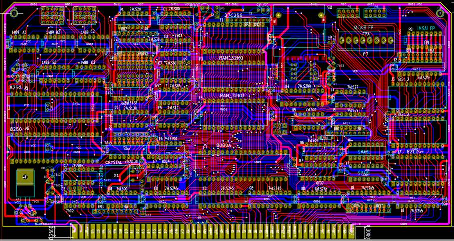
Well I'm finally done laying out this board. The autorouter only produced swiss cheese with over 900 via's. It looked terrible!
Anyway, I scrapped everything the autorouter did initially, and proceeded to layout the traces manually. Once I got what I thought was all the hard parts done, I let the autorouter have another go at it. Again it did not work out so well and it was unable to complete the board, so I proceeded to undo it's changes and/or improve it's routing manually. I squeezed those traces in there tight, any tighter and they'll be popping off the board. Anyway, I'm working on the silkscreen layer and ready to do a run.
Here's a picture of the board layout....
You can see the serial port connections on the top left, SD card to the right of the 27C256 EPROM, parallel ports next to that and the ALTAIR and IMSAI front panel connectors. There are also a few jumpers around the board to configure for CPU or Peripheral board only and ALTAIR/IMSAI mode. Firmware for the board will be my next project, but I have to make preparations for VCF-MW my priority. Dave Ruske and I will be doing a COSMAC 1802 exhibit there in September.
Cheers,
Josh Bensadon
From: crus...@hotmail.com
To: n8vem...@googlegroups.com
Subject: RE: [N8VEM-S100:3711] ALTAIR/IMSAI 8080 CPU replacement board
Date: Sun, 18 May 2014 00:57:20 +0000
Hi Guys,
Well, this project has just reached a milestone. The hardware is tested and working. I had some rewiring to do to make it work for the ALTAIR, I thought the ALTAIR and IMSAI front panels were (near) identical, but they are not.
There are some jumpers on the board to configure between ALTAIR and IMSAI.
Here's a picture of my debugging and testing setup. The board is being tested in the ALTAIR.
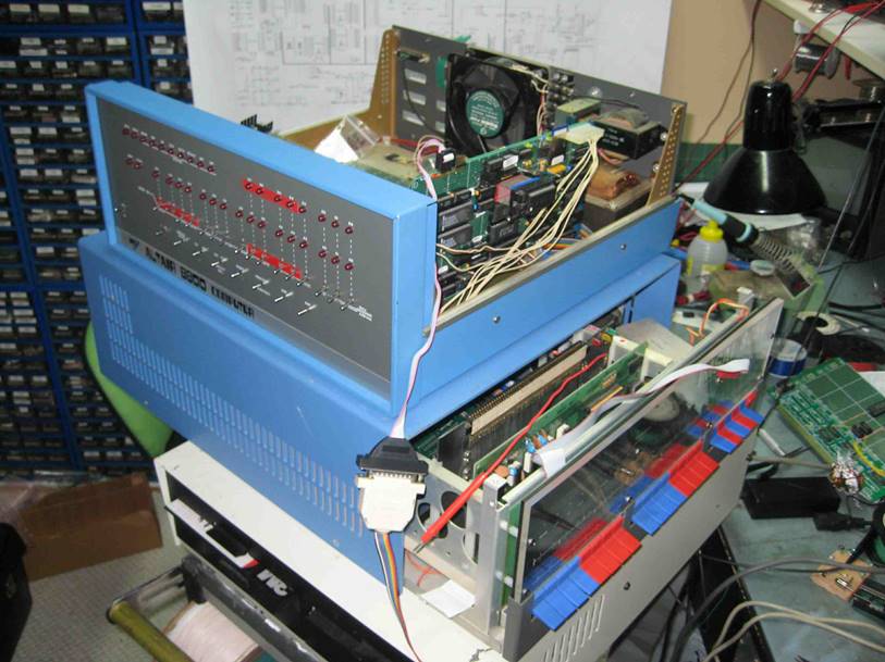
Now entering Phase 2... building a PCB.
Cheers,
Josh Bensadon
From: mon...@vitasoft.org
To: n8vem...@googlegroups.com
Subject: RE: [N8VEM-S100:3666] ALTAIR/IMSAI 8080 CPU replacement board
Date: Tue, 13 May 2014 13:56:05 -0700
Very nice Josh!
John
From: n8vem...@googlegroups.com [mailto:n8vem...@googlegroups.com] On Behalf Of Crusty OMO
Sent: Tuesday, May 13, 2014 1:19 PM
To: n8vem...@googlegroups.com
Subject: RE: [N8VEM-S100:3664] ALTAIR/IMSAI 8080 CPU replacement board
Hi Group,
Well, I'm cooking up this board at the moment. I have all the hardware figured out to run like the original CPU boards.
I need to do a little more testing of the hardware, then I'll proceed to building the boards.
The Memory, I/O, UARTs and SPI interface to the SD card appear to all be working.
8K chunks of memory can become either ROM, RAM or mapped off the board.
CPU: 8080A
UARTS: 2x 8250
RAM: 2x 32K
ROM: 32K
I/O: 8 input, 6 output pins
SPI to SD Card interface
ALTAIR & IMSAI Front Panel Connectors.
Where ROM is selected in a block it overlaps the RAM on reads, but writes go through to RAM.
The ROM can then be disabled and reads will come from the RAM at that location.
The firmware is copying itself to RAM then switching off the ROM.
The CPU can be deselected with jumpers and the board will work as RAM/ROM and I/O for another CPU on the bus.
Pictures attached. Yellow-Data, Brown-Address, Blue-I/O, Green-Control/Status & everything else.
Regards,
Josh Bensadon
--
You received this message because you are subscribed to the Google Groups "N8VEM-S100" group.
To unsubscribe from this group and stop receiving emails from it, send an email to n8vem-s100+...@googlegroups.com.
For more options, visit https://groups.google.com/d/optout.
--
You received this message because you are subscribed to the Google Groups "N8VEM-S100" group.
To unsubscribe from this group and stop receiving emails from it, send an email to n8vem-s100+...@googlegroups.com.
For more options, visit https://groups.google.com/d/optout.
--
You received this message because you are subscribed to the Google Groups "N8VEM-S100" group.
To unsubscribe from this group and stop receiving emails from it, send an email to n8vem-s100+...@googlegroups.com.
For more options, visit https://groups.google.com/d/optout.
--
You received this message because you are subscribed to the Google Groups "N8VEM-S100" group.
To unsubscribe from this group and stop receiving emails from it, send an email to n8vem-s100+...@googlegroups.com.
For more options, visit https://groups.google.com/d/optout.
--
You received this message because you are subscribed to the Google Groups "N8VEM-S100" group.
To unsubscribe from this group and stop receiving emails from it, send an email to n8vem-s100+...@googlegroups.com.
For more options, visit https://groups.google.com/d/optout.
--
You received this message because you are subscribed to the Google Groups "N8VEM-S100" group.
To unsubscribe from this group and stop receiving emails from it, send an email to n8vem-s100+...@googlegroups.com.
For more options, visit https://groups.google.com/d/optout.
--
You received this message because you are subscribed to the Google Groups "N8VEM-S100" group.
To unsubscribe from this group and stop receiving emails from it, send an email to n8vem-s100+...@googlegroups.com.
For more options, visit https://groups.google.com/d/optout.
--
You received this message because you are subscribed to the Google Groups "N8VEM-S100" group.
To unsubscribe from this group and stop receiving emails from it, send an email to n8vem-s100+...@googlegroups.com.
For more options, visit https://groups.google.com/d/optout.
--
You received this message because you are subscribed to the Google Groups "N8VEM-S100" group.
To unsubscribe from this group and stop receiving emails from it, send an email to n8vem-s100+...@googlegroups.com.
For more options, visit https://groups.google.com/d/optout.