Introduction Many S-100 board manufactures had their own Video boards. Most initially were character based "video TTY's". The very early ones were restricted to 64 characters/line (for example the SSM board) but soon 80 characters per line became common. A good example is the SD Systems 8024 Board.
As time went on, boards started to get more sophisticated and began to offer fairly high resolution graphics capabilities. A good example of this would be the Matrox ALT512 board which offered color graphics at a 512 X 256 resolution. There were even a few of higher resolution. The NEC 7220 based video controller boards for example, which brought video display graphics to a new level. That chip was the NVIDEA chip of its day back in the early 1980's.
Once the IBM PC appeared on the scene video hardware compatibility with it became key. There were a few S-100 bus attempts to make equivalent cards. The Lomas "Color Magic" IBM-PC Color Graphics Adaptor (CGA) look-alike probably being the most successful. However with the phasing out of the S-100 bus in the late 1980's, no higher resolution S-100 video boards were ever produced.
On the IBM-PC side of things (and its clones), video boards of increasing resolution appeared, eventually culminating in "VGA" boards. At the same time a very long list of "all in one" PC video chips were developed. The firm Chips and Technologies was the first company (outside of IBM) to deliver a compatible VGA chipset, the 82C451. This market was then entered into by companies such as Trident Microsystems, Western Digital, Cirrus Logic, Oak Technologies, and others, until it was saturated. None of them exist today, nevertheless they started a whole industry of powerful all in one video chips. With one chip, a little DRAM and a ROM a complete video board could be constructed with outstanding capabilities.
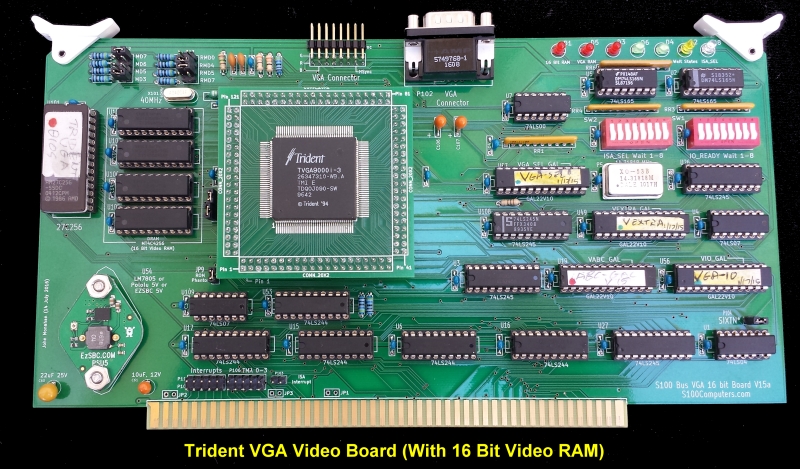
With the recent of our introduction of our 16 bit 80486 based S-100 boards and MS-DOS based operating systems there is a clear need for a good high resolution 16 bit VGA style video board. The specifications of a VGA board is beyond the capability of discrete 74LSxx based TTL chips. This is the job of a dedicated "Video Controller Chip". What chip should one use ? There are a number of candidates.
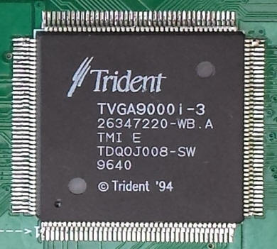
In the end I settled for the TVGA9000 made
by Trident Microsystems. Major points in its favor were SVGA resolution, an onboard DAC, an excellent manual describing the chip and reasonable availability. The only catch is that it only exists in a 164 pin surface mount version -- as do all these video chips.
See here
also for more information about this chip.
A while back I constructed an 8 bit video RAM version of the board for use with
our 8 bit 8088 CPU board.
With that CPU the board worked fine. Moving to a 16 bit RAM interface would
appear simple. However after numerous prototypes and approaches I
concluded that interfacing such a chip to our
8086,
80286 and
80386 CPU boards
was not possible with the layout on those boards. The Trident (and other
VGA chips like it) require the capability of the CPU circuit to accept 16 bit
data in two back to back bytes. This requires the CPU board to monitor the
S100 bus signal SIXTN* to see if the target board of the CPU can accept 16 bit
data. Normally this is not a problem since all our S100Computers (and
later S100 bus boards of the 1980's) could work with 16 bit data.
Fortunately the 80486 CPU has the internal capability to talk to an 8, 16 or 32
bit data bus transparently "on the fly". We have here an upgrade then of
the earlier 8 bit Trident VGA board to allow the board to work with 16 and 8 bit
video RAM and our 80486 CPU board. Video RAM is faster not only because of
the 16 bit data path but also because this board normally requires no wait
states from the board itself.
TVGA9000 General Information
The TVGA9000 according to Trident Microsystems is a versatile
and full-featured single-chip solution for VGA (Video Graphics Array) systems.
The chip provides register-level compatibility, enhanced graphics and text
modes, support for 256Kx4 DRAMs, plasma display control; and support for analog
VGA, , EGA, CGA, and MDA monitors. The chip provides register-level
compatibility with standard IBM VGA modes and backward compatibility with EGA,
CGA, MDA. and Hercules modes. The enhanced graphic and text modes provide
high-resolution displays in 4, 16, and 256 colors. Support for 256x4 DRAMs saves
board space and provides cost savings.
Display support for analog VGA. digital VGA, plasma, EGA, CGA, MDA. and Hercules
monitors assures that the TVGA9000 board solution may be used with virtually any
monitor on the market.
Compatibility
The TVGA9000 supports both the PC/AT bus and the PS/2 Micro Channel bus. The
TVGA9000 is fully compatible with all standard IBM VGA modes and EGA. CGA. MDA,
and Hercules modes, and allows the following: Use of all application software
for VGA. EGA, CGA, MDA, and Hercules modes Emulation of EGA, CGA, MDA. and
Hercules modes on a VGA monitor.
Text Modes Extended Graphics and Text Modes Extended graphics
modes supported by the TVGA9000 include the following:
64Ox400, 640x480 and 800x600 in 256 colors from a palette of
256K116M.
800x600 and 1024x768 (interlaced or non-interlaced) in 16
colors from a palette of 256K116M.
1024x768 in4 colors from a palette of 256K/16M.
Extended text modes offer 132-column text with 25, 30,43. and
60 rows.
This chip is clearly an almost self contained XVGA board. The only
major support chips are a 27C256 BIOS EPROM and four 4X256K DRAM chips.
The datasheet for the chip can be obtained
here.
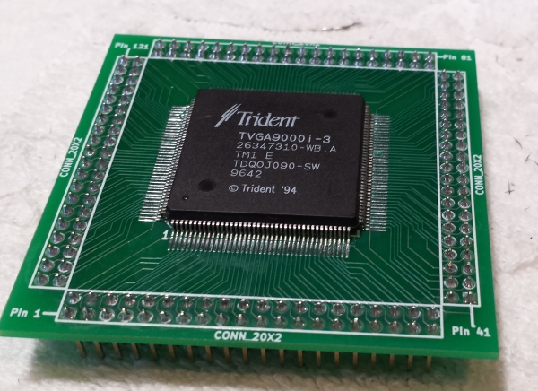
Unlike the 8 bit VGA board I
decided to use a 160 pin surface mount converter miniboard to mount the video
chip. This "adaptor" has extra long solder pads so soldering the Trident
VGA chip to the adaptor board is very easy.
To do so, first apply plenty of
solder flux paste to the pads, then with a fine tipped solder tip run solder
along all the pads. It will bulge up on the pads themselves with no bridges.
Next place the Trident chip on the pads. Carefully aligned the
chip so all pins are aligned. Then solder (only) pin 1 by lightly pressing down
on the chips pin. Next do the same for pin 81. Very carefully look
around the chip and be sure each pin is aligned up exactly with it's pad.
Use a sharp blade between pins to reposition a pin if necessary.
Then go around the chip by simply touching the boards solder pads at the end of
each pin. The solder will quickly weak up under the pin. No more than a
half a second is required. It actually becomes quite easy to do.
Afterwards spray the area with flux remover and inspect each pin under a
magnifying glass/light by trying to move a pin with a blade edge. It should not
move.
These 160 pin adaptors can also be obtained commercially (e.g..
Proto-Advantage.com). However those adaptors have the normal small
solder pads. If you are good at soldering SMD chips this is not a problem.
Using an adaptor also allows one to better space components on the S100 board
because the VGA video circuit can lie under the VGA chip itself.
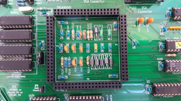
You do not actually have to use the four 20X2 sockets on the board,
while not
recommended, you can press the adaptor pins directly into the holes on the
S100 board. The connections are tight enough at least for testing. Once
completed however I recommend soldering the adaptor in place. With or
without the board 40X2 sockets, the height of the board is still within a standard
S100 bus motherboard spacing.
The third reason for using an adaptor is that in the future I intend to use
other VGA chips. In theory at least, the same S100 board can be used.
This may not be possible, don't count on it however.
The KiCAD data, schematic and GAL files for the board are given below.
I decided to stick with the 4 GAL chip approach used in our 8 bit VGA board
rather than use a 1508 CPLD. One could go either way. At least with
GAL's one
does not need a CPLD programmer for this board. Most modern ROM
burners also burn GAL's.
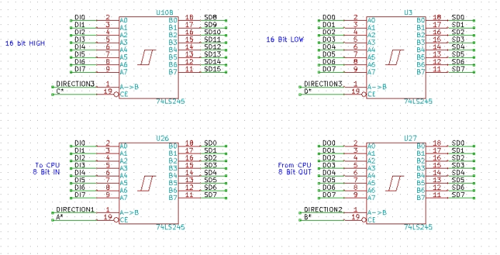
I used the following schematic for data transfers.
DIRECTION_2 = /bpWR ;HIGH, WRITE 8 bits, U27, Set pin 1 direction A -> B
/C_SIGNAL = bsMWRT * ISA_SEL * /bpWR * /bsXTRQ * /MEMCS16 ;WRITE 16 bits via
U108 for video RAM
+ bsOUT * ISA_SEL * /bpWR * /bsXTRQ * /IOCS16
+ bsMEMR * ISA_SEL * bpDBIN * /bsXTRQ * /MEMCS16 ;READ 16 bits via U108 for
video RAM
+ bsINP * ISA_SEL * bpDBIN * /bsXTRQ * /IOCS16
/DIRECTION_3 = bpDBIN ;U108
& U3, Set pin 1 bi-direction for video RAM
/D_SIGNAL = bsMWRT * ISA_SEL * /bpWR * /bsXTRQ * /MEMCS16 ;WRITE 16 bits via U3
for video RAM
+ bsOUT * ISA_SEL * /bpWR * /bsXTRQ * /IOCS16
+ bsMEMR * ISA_SEL * bpDBIN * /bsXTRQ * /MEMCS16 ;READ 16 bits via U3 for video
RAM
+ bsINP * ISA_SEL * bpDBIN * /bsXTRQ * /IOCS16
/X16_LED@ = ISA_SEL * bsXTRQ ;Flash LED indicating a 16 bit board request
/SIXTN@ = ISA_SEL * /IOCS16 ;Indicating to S100 bus Trident chip can handle 16
bits
+ ISA_SEL * /MEMCS16
/ISA_SEL_LED@ = ISA_SEL
;Board select signal Those with some experience will see that the above
code and chips are in fact somewhat redundant. One could program the above into
3 buffers, but since the is no shortage or real estate on this board I went with
the simple direct approach. The GAL code for this board for the
"VGA_IO_GAL", ISA_SEL_GAL" EXTRA_GAL" GALs is identical to the GALs on the
8 bit VGA board.
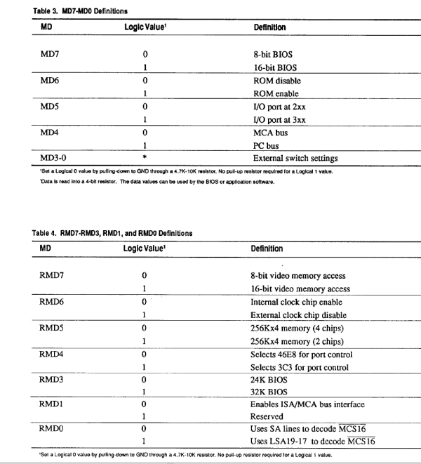
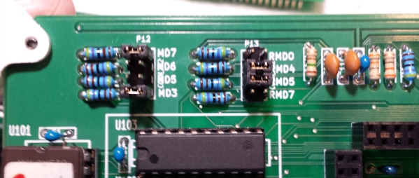
However the "ABC_GAL" code is different. The Trident chip has a number of initial startup configuration options. A
number of these are brought out to the jumpers on P12 and P13.
Here is the default configuration:-
For those that wish to experiment, jumpers p12 5-6 and JP9 should allow you to
disable the onboard ROM and use an external RAM based BIOS. I have not
succeeded in getting this to work so far.
Board Construction
There is nothing particular special about constructing this board. Use
the normal construction process we have in the past. For example test
the orientation of the LEDs by grounding the pins of U56
and U57 (without any board IC's) . You can use an old 5A LM7805 voltage
regulator or the newer Pololu or EzSBC 5V switching regulators. There are
footprints on the board for all three types. However the solder holes for
the EzSBC 5V are slightly too close. Very carefully bend the two pins inwards
and space the regulator away from the board with a washer. Remember these nuts
act as a ground for the regulator. Make sure they are tight.
Check the voltage before adding IC's. Be careful to get the capacitor
orientations correct. Don't forget R5 under U108.
Add everything except the Trident
chip first. The RAM and ROM LED's, D1 and D8 should flash with the 8086 memory map "A"
command around the address range A0000-CFFFFH. If not check the programming of the
U56, U57 or U19 GALs. Be sure to insert jumpers JP9, P104 and P14 1-2 & 3-4.
BTW, I considered using an EEPROM (a 28C256) instead of the UV 27C256, (would
need two reconfiguration jumpers), I stuck with the high
speed UV chip (Jameco #29714 or #140476) however. If I get the
Cirrus Logic GD5420
driven board to work I will add that option.
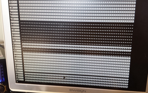
With the Trident chip
present, the memory map should look like this:-
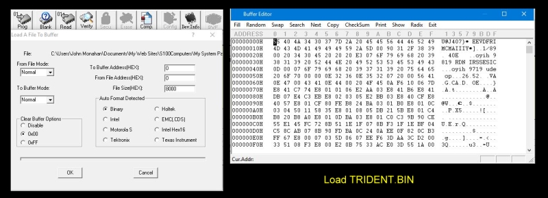
The VGA BIOS code resides in U101. Its a binary copy of the BIOS from a 1993
Diamond Inc. "Speedstore Pro" ISA PC VGA Board. The Binary file is supplied
below. You "burn" it directly into a 27256 or (better) 27C256 PROM.
Here are the relevant pictures for the Wellon VP290 Programmer.
Note because of the strange way the VGA chip accesses a single ROM, the ASCII
display of the data shows only every second byte. Even bytes are in the lower
half of the ROM, odd bytes in the top half.
VGA Board Bugs/Notes Please note this board will only work with our
8088,
Baby and Full Size 80486 CPU
boards. It will not work with our
8086,
80286 or
80386 CPU boards.
The latter boards do not recognize the S100 bus signal SIXTN*. This signal is
returned to the CPU board if the target S100 board (RAM or I/O board) cannot
process a 16 bit data word. All our previous S100 boards can, and do,
process 16 bit data with no problems. However these VGA chips actually
require the ability (upon initialization) to process 16 bit requests as two back
to back 8 bit requests. Our earlier CPU boards (and most old S100 bus
8086/80286 style CPU boards) cannot do this. The 8088 and 80386 CPU do
this internally within the CPU and so work fine.
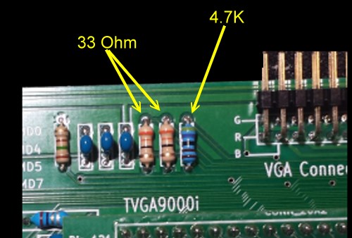
There is an overwrite on the silk screen for the resistors R111, R112 &
R110 at the top left of the board making the values hard to read.
Their values are shown here.
If you are pushing the 80486 to high clock rates try and have this board near
the 80486 CPU board in the S100 bus. A characteristic of the board not
responding correctly is the appearance of random white character squares on the
screen with a screen scroll. This can happen with a large 20 slot
motherboard in particular. If it persists reduce your CPU board oscillator clock
rate.
For high CPU clock speeds if you can, use a fast UV EPROM such as the AMD 27C256-55 (55ns), e.g. Jameco
266079. Somewhat to my surprise I found it works best at high speeds with
74LS245 bus drivers rather than 74F245s.
I currently have 3 of these boards running. On one, very occasionally the
Trident chip on power up does not initialize completely and comes up with a
green background screen instead of the normal black background. Hitting
reset always corrects the problem. I suspect the delayed reset pulse with
R102 & C104 needs to be tweaked.
Our MSDOS support board supports most MSDOS programs right out of the box.
However it does not contain an 8237A DMA controller found on the IBM PC
motherboard. Any VGA software that utilizes that chip will not work correctly in
our system. The only common (at the time) MSDOS program I have tried with
the board that had this requirement was the DOS program "WindowDOS", a directory
display program. I have thought of doing yet another MSDOS support board
(a V4 version) with a DMA controller chip onboard. I'm open to opinions,
however I may wait until I get a PDP-11 CPU S100 board working because that
system makes extensive use of DMA.
Otherwise no hardware bugs have
been seen for this board to date. It boots up MSDOS (V4.01) fine.
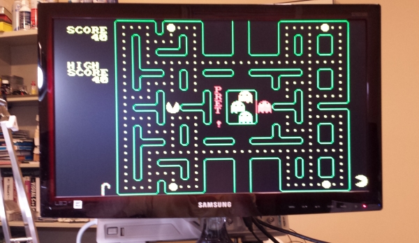
There seems to be a software problem in the 80386/80486 ROM BIOS when running the board in the
old IBM PC CGA board low graphics mode with programs like "PACMAN". The
graphics appears fine for the 8086/8088 BIOS. If somebody has time perhaps they
could dig into this. I suspect it has to do with the initialization of low
RAM in the 80386 BIOS code. Here is a picture of the Pacman initial screen
you can download from here.
Here is a short video showing the booting of MSDOS V4.01 on the VGA board.
A Production S-100 Board.
Realizing that a number of people might want to utilize a
board like this together with a group of
people on the
Google
Groups S100Computers Forum, "group purchases" are made from time to time.
Please see here
for more
information.