S100 banner

Home S-100 Boards History New Boards Software Boards For Sale
Forum Other Web Sites News Index    

The Super IO Board II
     
  Final Board with Chips

Introduction.            

S100Computers has a number of well established IO boards by now. All are fairly well debugged and seem to function correctly. Some are almost 10 years old by now. Since that time the have been a number of advances in small computer interfaces.  Boards like the Raspberry Pi or Arduino series have revolutionized computer interfacing.  Many add-on "modules" have been developed that allow quite powerful computer setups. There is no reason why these modules cannot be incorporate into S100 Bus Systems as well. We have now the new Super IO board that has many IO interfaces/modules.   However it requires a Cyclone IV FPGA module and programming.  These FPGAs have become 10X more expensive these days because of supply problems.  I decide to also provide an "FPGA free" version of the board which I will call the Super IO Board II.   It has the following capabilities.

1.    A generic RS232 Serial port capable of operation up to 115,200 Baud with a DB9 Connector and a 8X2 Pin Connector
2.    A USB IO port available on the S100 Bus for general use.
3    A Centronics compatible printer parallel port.
4    A RC Systems V-Stamp speech synthesizer
5.   Two 8255As with a total of 6 port parallel I/O ports
10.  An Adafruit FX Sound Board output
11.  A DFRobot MP3 Player output
13.  A 555 chip based pulse circuit
14.  A 8 LED indicator array.
15.  An 8 bit input configuration switch.
17.  A local WiFi interface (ESP 8266) connection

For the serial port t
he default baud rate for this connection is (38,400 BAUD, 2 stop bits, no parity). 

Step By Step Building the Super IO Board
The build instructions are fairly simple for this board but because it is a complex board building it should not be rushed.  As always, first examine the bare board carefully for scratches or damaged traces, use a magnifying glass if need be.  A broken trace is almost impossible to detect by eye on a completed board.
   
Solder in all the required IC sockets, resistors, resistor arrays, capacitors, jumpers, and the Pololu 5V and 3.3V voltage regulators.  Please be sure you put the resistor arrays in with the correct orientation of pin 1, (the square pad). An incorrect orientation is one of the most difficult things to detect/debug on a board if not noticed. Check their values before soldering (they are difficult to remove).  Insert all jumper arrays.  

There appears to be a few variations of the 74LVC245 20 pin DIP level Shifters chips with "A", "AN" etc. after the 245.   As best I can tell so long as they are 20 pin DIPs they are all OK. I use either Mouser chips # 595-SN74LVC245AN.  

I use the Adafruit USB serial Adaptor, but the equivalent SparkFun unit also works fine.

It is absolutely essential you use three Zilog 85C30's.  I could not get the board to work with other UARTs such as the OKI equivalent.  The reason for this is unclear to me.
   
   Zilog 85C30
   
Note there are two sockets for the Pololu 5V and 3.3V regulators. While the older ones (D24V25F5 and
D24V25F3) are still available and use P3 and P4, it seems Pololu is suggesting users use the newer D24V22F5's (5V, 2.5 Amp) units, it has a different pinout, use this one in P2 (not P3).  More recently they also added the equivalent D24V22F3 3.3V regulators. Unfortunately in their wisdom they again changed the pinout connections. You must use the Pololu D24V25F3 3.3 V regulator in P4 or the D24V22F3 regulator in P21.   Be sure you get these regulators/ correct. To be safe once inserted, check the voltage in your system on a 5V and 3.3V IC, (see the schematic) with no chips yet inserted on the board. 5V and 3.3V going to the correct pins of the FPGA adaptor.  (5V going to the 3.3V pins will blow the unit!).  Please note Pololu has come out with more 5V and 3.3v regulators.  Please examine the pinouts and match them with the board sockets.  Unfortunately the newer 5V and 3.3V units look exactly the same on the surface. Presumably some of the internal resistors are different to give 5V and 3.3V.

Note recently the above Pololu regulators have gotten hard to find and have become expensive.  Pololu now has more options to pick from.  Examine the pinout of any of their 5V or 3.3V  regulators and place them in one of the two sets of slots above.  You can also use the EZ-SBC regulators. These are currently cheaper and as best I can tell just as good -- though they have a larger footprint however.

When adding the LED's be sure to orient them correctly. (Usually the longer lead in the square pad). However for the timer LED (D13) the longer LED lead should go into the circular pad hole not the square one.
Do not install a socket for U23 (the 74LS123 chip under the speech synthesizer).

At this point insert the board into your system and check your S100 bus Z80 monitor boots fine.  If not check for solder bridges etc. Also do one last check to be sure every IC solder pin is soldered.  Seems trivial, but I don't know how many times I got caught with this error.
 
 Here is a picture of (a prototype version) the board at this stage:-
   
  Board without chips
     

Place the board in the S100 bus and check you are getting 5 volts on U3 pin 14 and 3.3 volts on U4 pin 20.

Next install all the IC's on the board.  Solder in directly U23.  Do not install any of the sound modules yet.

IEEE-696 16 bit S100 bus port IO addressing is assumed (the upper 8 lines being zero) for this board. This can be easily bypassed within the FPGA (Jumper
K2 1-2).  Do so if your CPU board does not zero the high address lines for port I/O. To be safe we will jumper K2 1-2 for now. Note 16 bit CPU's will probably require K2 2-3.  Jumper K1 1-2.
 
Install a Sparkfun FT231x USB adaptor in
P11.  Note it has a jumper on its back for 3.3V operation, use 3.3v not 5V. You can solder the adaptor directly to the board or use sockets.  See the section above on soldering sockets. I suggest direct soldering.  Note the USB FT231x  adaptor actually has 3 sockets. The two side ones are not used here and are only there to steady the adaptor on the board. I use only pin 1 in each case. You can also use the Adafruit CP2104 USB adaptor equivalent adaptor.  Perhaps it's just me,  but sometimes I've had problems getting this adaptor to link up with my PC's.
I like to use the same USB adaptor for my PC connection on many boards.  You can often get by simply pressing the USB adaptor pins into the board holes without solder.  This way you can move the same adaptor around and not have to reconfigure your PC TTY terminal software each time. If flaky use a socket or solder!

The default software on this board assumes a USB port running at
38,400 BAUD, 2 stop bits, no parity.  (This can be changed within the SIODIAG2.ASM file below).  There are a number of Windows/PC programs you can use to receive and display the data.  I like Absolute Telnet  from Celestial Software, but others are free.

Here is a picture of (a prototype version) the board at this stage:-
   
  Board with Chips

 
The Super IO Board Diagnostic Program
There are a lot of "moving parts" on this board.  A good diagnostic program running on the S100 bus is required to debug each component.  SIODIAG2.ASM does this. It is menu driven with a sub menu for each component.  It should be run at
100H in the S100 bus RAM. There is an equate in the code to also allow it to run with a CPM BIOS. You can load it across from a PC using the Z80 Monitor "X" command  or within CPM with PCGET.

Here is the
SIODIAG2.ASM Signon Menu:
      
   Monitor Signon

The RS232 Serial port.

This circuit is identical to the serial port we have on our Serial IO Board. There are actually two connections. A "classical" DB9 socket and a 10 pin header. The pin-out is identical to that on the Serial IO Board.

For most PC serial ports the only signals you really will need to download/upload data are:-
TXD, RXD, CTS and RTS.  You will need to cross these signals as follows:-
 
  
   RS232 Pinouts
    
There are two types of RS-232 Sockets. The older 25 pin sockets and the newer smaller 9 pin sockets. Unfortunately the pin designations are different for each type.   The Clear to Send and Request to Send lines are required in particular on the S-100 side of the connection to prevent data getting lost while the CPU is busy. If you  running a system at less than 1200 Baud even they are usually not required.

The board has the CTS, RTS, DCD and DTR signals .  All four signals are converted to +/-12 Volts by
U15 (a MAX 232).  (Be careful with a logic probe on these signals).
 
The easiest way to test a RS232 port is to do a 'loop around" test.  The output Tx signal from the port is connected to the Rx signal, an RTS is connected to CTS.
Jumper
P17 3-2 and 9-8

Launch the SIODIAG2.ASM diagnostic program and use the "
R" command. It will initialize the Zilog 8530 UART (U7) to 38,400 BAUD, 2 stop bits, no parity
After connecting the serial port to a TTY terminal on your PC it should signon as shown above.
If you use the P17 connection use the RS232 lines shown in the schematic (and for the Serial IO Board).
If you use the DB9 socket, jumper P17 1-3,2-4 and 8-9.
Here is what your PC TTY window should show:-
           
    RS232 Test
     
Then anything you type on the PC TTY terminal should echo back.  If this does not happen check the connections.  Next remove the MAX 232 chip (U15) and jumper its pins 9-10 and 11-12. 

The Parallel Printer Port.
This circuit is identical to the parallel port we have on our
FPGA Z80 SBC Board.
Bring up the SIODIAG2.ASM
Diagnostic program and use the P menu option to send a test string to the printer.  These days many printers use a USB connection instead of a Centronics printer port.  You can use one of the common Centronics -> USB port adaptors instead to test the port.
When connected properly the two printer LED's should light up.
   
    Printer LED's
 
Here is what the SIODIAG2.ASM test printout
"P" command should look like:-
  
    Printer Test


The USB Port.
The S100 bus Serial IO Board has a serial port at 
28H and the data port at 29H, so here we will use a USB status port of 8CH and a data port of 8EH (for UART #2).
Use the
SIODIAG2.ASM Program "T" Command to test  a PC USB port TTY program at 38,400 BAUD, 2 stop bits, no parity.
  
    USB Port Connection

You can examine the routines
USB$CO, USB$STATUS and USB$CI in  SIODIAG2.ASM to incorporate the port in your other programs.
Remember these are S100 bus assembly modules. You can use the above code in any program.
Please note for some reason both the Adafruit and Sparkfun USB modules do not accept keyboard characters from the USB terminal
unless the adaptor CTS is connected to RTS (P40 pin 2 to pin 6). Do this on the back of the board. 
I have not figured out what the problem is.


The RC Systems V-Stamp Speech Synthesizer
In the late 70's primitive Voice Synthesizer chips started to become available. A popular S-100 board was the Computalker CT-1 board.
Things have come a long way since them. Not only in the size of the chips but the quality of the speech. 
 
  V Stamp Picture
V-Stamp Voice Synthesizer

Today very realistic speech can be generate with a single chip IC.  One particular system that I like is the V-Stamp system by RC Systems. It is based on their RC8660 chip set.  See here for a complete description. The 24 pin package behaves as an idiot proof black box. You send simple ASCII text strings to the chip over a serial line (5 Volt, TTL level signals).  Once the chip receives an ASCII 0DH (CR), it speaks out the string with amazing intelligence.  Numbers, for example, are pronounced in full (32,800 Baud is spoken as thirty two thousand eight hundred Baud).   The chip even has circuitry to figure out the communication Baud rate automatically on reset.

Debugging is easy! In RAM at 0H:-
3E 33
D3 88         ;This assumes the Zilog UART #1 Serial port B is 88H and is being used to communicate with the chip and the Zilog chip U7 is initialized.
3E 0D
D3 88
C3 00 00


This sends "3" followed by a CR to the chip. It says the number "3".
Please note this assumes the Zilog SCC chip has already being initialized. See the code in SIODIAG2.ASM as to how to do this.
The default Speech Serial IO ports for the Zilog 8530 UART
#1, U7 are 88H and 8AH.
If you want to keep the S100 Speech Serial board in your system to be the same as the Serial IO Board use
A0 and A2H for the Z8530 U7 chip here
There is an equate in the SIODIAG2.ASM program to set the UART address range. Remember you must always initialize the Zilog UART before using it.

The chip and board must be connected to an external speaker/amplifier
P31
Once you start adding voice feedback to your programs you find yourself always doing so.
You can send information in voice form that will not upset the current CRT display. Quite useful.
 
The V-Stamp chip can be obtained here from RC Systems.  They have a 3.3V and 5V version. I use the 5V version (2 min speech storage capacity,  #RC860F-1C). Unfortunately it is not cheap ($75), but it's an amazing device. 

One other point, the pins on the V-Stamp "chip" are quite thick.  I used a 28 pin DIP socket cut in half to seat the chip. Be sure beforehand the socket will accommodate the pins. Some Auget sockets will not.   However as for the USB adaptor you may find the module fits tight in the board holes without any socket or solder.  The two rows of pins are very slightly too wide to make a tight connection. Place one row and leaver the module upward to seat he second row.  If you must use a socket use the Jameco female headers #308592 (cut to size) or a 40 DIP pin socket sides (cut to size).

You can test the chip with the SIODIAG2.ASM using the "
S" menu command.


The 8255A I/O Ports.

These chips,
U9 and U13 are very well used chips on our S100 boards. Each has 4 I/O ports. The first 3 (A,B & C)  are configurable by its Port D.  They can be input, output or bi-directional depending on what is sent to ports D. 
For example if you send
80H to port D then ports A,B & C are configured as 8 bit output ports. The three 8 bit I/O pins are available at P4, P14 and P11.  See the datasheet for an 8255A for more information.
The parallel printer port is Port A of
U13 and the Dip switch input SW1 is port B of U13.
I assume mostly users will know how to configure, use these ports by now.


The Adafruit FX Sound Board
  
    FX Board Picture
  
This is the first new circuit we will add to this board.  It will allow you to add audio/sound effects to your next S100 bus project without an Arduino or Raspberry Pi board. Up until now it has been very hard to find a simple, low cost audio effects trigger circuit that is easy to use and does not require any external module programming. There's all sorts of tricks with ISD chips or recordable greeting cards out there, but they never sound any good. The Adafruit Sound Board is a very nice solution.
  
The Sound Board has a lot of amazing features, you don't even need an SD card, there's 2MB or 16MB of storage on the board itself, so you can store up to 15 minutes of quality compressed audio. (Double that if you go with mono instead of stereo). There is a built in Mass Storage USB port,  so you can drag and drop sound files on as if it were a USB drive.   You can use compressed
Ogg Vorbis files for longer audio files, or uncompressed .WAV files.  Up to 11 Triggers can be connect up to 11 buttons or switches, each one can trigger audio files to play,  or you can send commands from the S100 bus system. Also there are  Five different trigger effects - by changing the name of the files, you can create five different types of triggers which will cover a large range of projects without any programming.

This is a fairly complicate device to understand with many options.  You should read in detail the Adafruit manual before working with it. See here.

  • It is a completely stand-alone unit, it just needs a 3 to 5.5VDC power supply.
    You don't even need an SD card, there's 2MB or 16MB of storage on the board itself.
    You can store up to 15 minutes of quality compressed audio. Double that if you go with mono instead of stereo.
    There is built in Mass Storage USB on the device. Plug any micro USB cable into the Sound Board and from your computer you can drag and drop your files right on as if it were a USB key.
    It utilizes Compressed or Uncompressed audio - Go with compressed Ogg Vorbis files for longer audio files, or uncompressed WAV files.
    High Quality Sound - You want 44.1KHz 16 bit stereo? Not a problem! The decoding hardware can handle any bit/sample rate and mono or stereo.
    There are 11 "Triggers" - Connect up to 11 buttons or switches, each one can trigger audio files to play (or use jumpers to one of the boards parallel ports).
    Stereo line out - There's a breakout for both left and right channels, at line level, so you can always hook up to any kind of stereo or powered speaker
    Five different trigger effects - by changing the name of the files, you can create five different types of triggers. This will cover a large range of projects without any programming.
        
Install the Adafruit FX module in its sockets
P28 & P30
Its best to listen to the boards output using the boards stereo headphone socket.

To use the module onboard  speaker jack to connect up head phones or a speaker. As for the USB adaptor and speech synthesizer,  you may find the module fits tight in the board holes without any socket or solder.  The two rows of pins are very slightly too wide to make a tight connection. If you must use a socket use the Jameco female headers #308592 (cut to size) or a 40 DIP pin socket sides (cut to size).

In order to fully utilize this module you need to study the manual in detail, see here before going any further.

You need to download the very simple basic sound files at the bottom of this page for testing.  Hookup the USB port to your PC (it appears as a drive), and drag the files across.
Launch the Super IO Board Diagnostic Program and open the
F sub menu.
Here is how it should appear:
    
    FX Board Menu FX adaptor

Most of the options are self obvious.  When the sound says "
track x" that's just a filler for a sound track you would add. 
To start use menu 0 to list files and 7 to play a file  (e.g.
SAMPLE2.OGG).  
Please read the Adafruit manual to go further there are many options available with this board hooking up to the boards pins with a cable/switches..

  • The module has 11 "Trigger pins"  connected up to the P30 header (see below).
  • There are 5 different "Trigger effects".  By changing the name of the files, you can create five different types of triggers which will cover a large range of projects without any programming


What is mean by trigger effects? Well, depending on your project you may need to have audio play in different ways. Adfruit thought of the five most common needs and built it into the Sound Board --  so you just rename the file to get the effect you want. See the product tutorial for more details
  1. In summary:
  2. Basic Trigger - name the file Tnn.WAV or Tnn.OGG to have the audio file play when the matching trigger pin nn is connected to ground momentarily
  3. Hold Looping Trigger - name the file TnnHOLDL.WAV or .OGG to have the audio play only when the trigger pin is held low, it will loop until the pin is released
  4. Latching Loop Trigger - name the file TnnLATCH.WAV or .OGG to have the audio start playing when the button is pressed momentarily, and repeats until the button is pressed again
  5. Play Next Trigger - have up to 10 files play one after the other by naming them TnnNEXT0.WAV thru TnnNEXT9.OGG.
  6.                                 Will start with #0 and each one on every momentary button press until it gets through all of them, then go back to #0
  7. Play Random Trigger - just like the Play Next trigger, but will play up to 10 files in random order (TnnRAND0.OGG thru TnnRAND9.OGG) every time the button is pressed momentarily


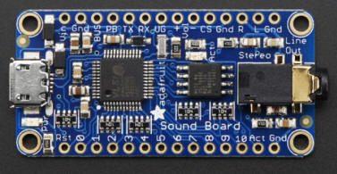
The sound board is designed to be simple: it does not have polyphonic ability, can't play MP3's (MP3 is patented and costs $ to license, so this board uses the similar but not-patented OGG format, there's tons of free converters that will turn an MP3 into OGG), isn't reprogrammable or scriptable, and you can't have any other kind of trigger type. However, there's a good chance the project you want to make will work great.


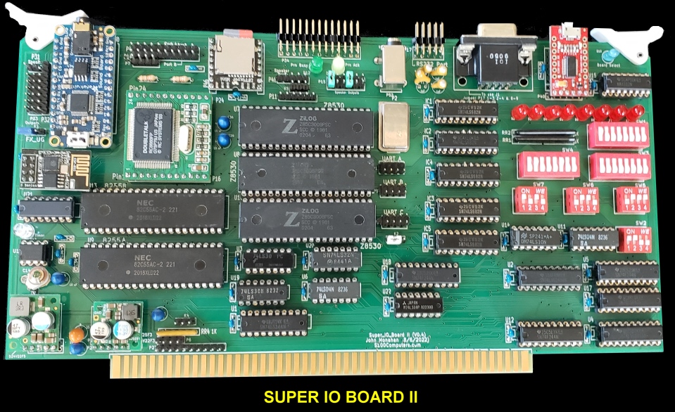
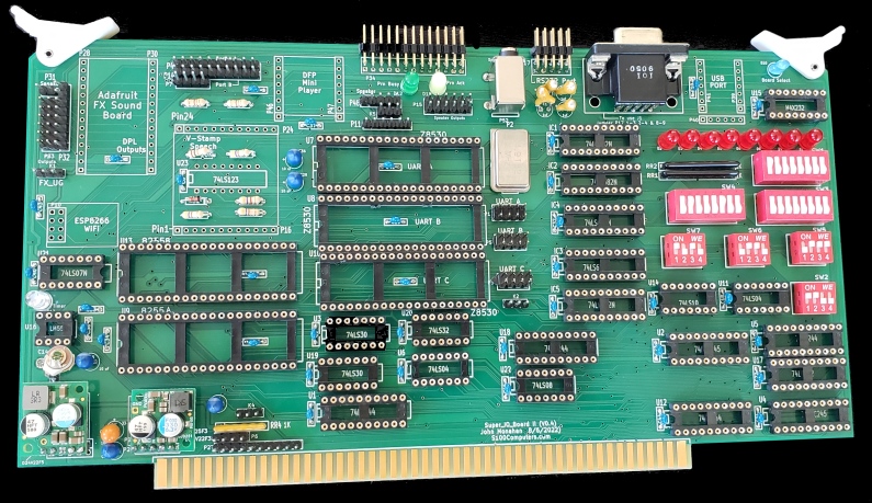
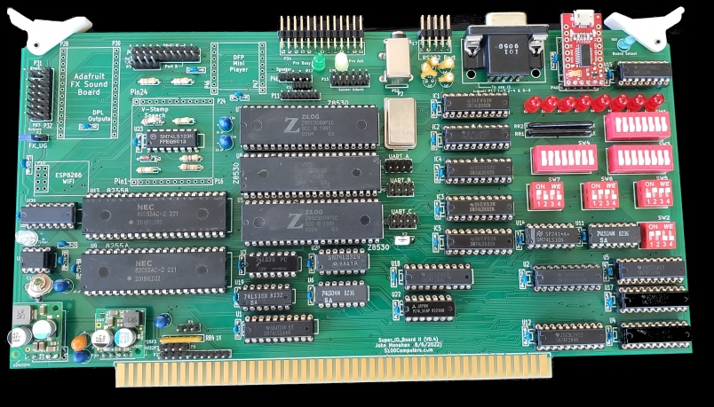
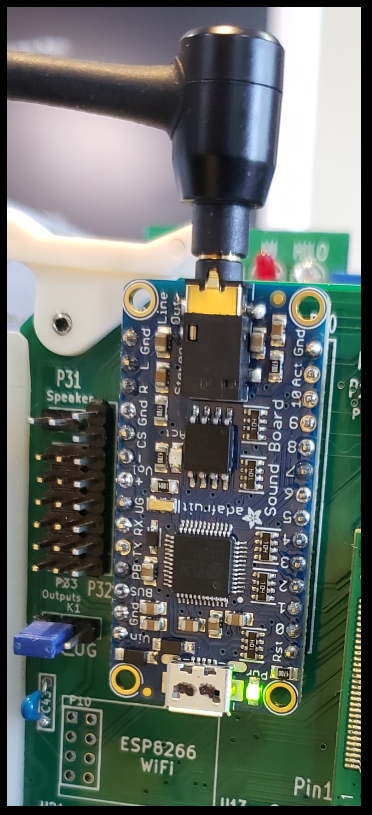
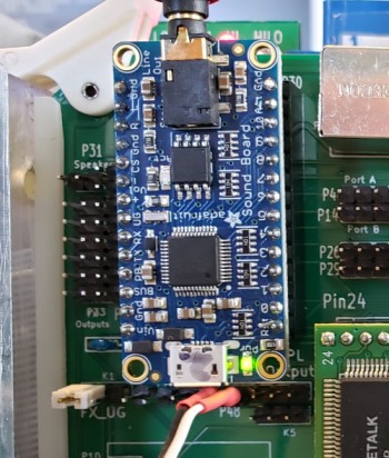
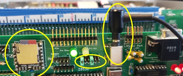
Adafruit designed this board specifically for people who wanted to make props, costumes, toys, and other small portable projects.
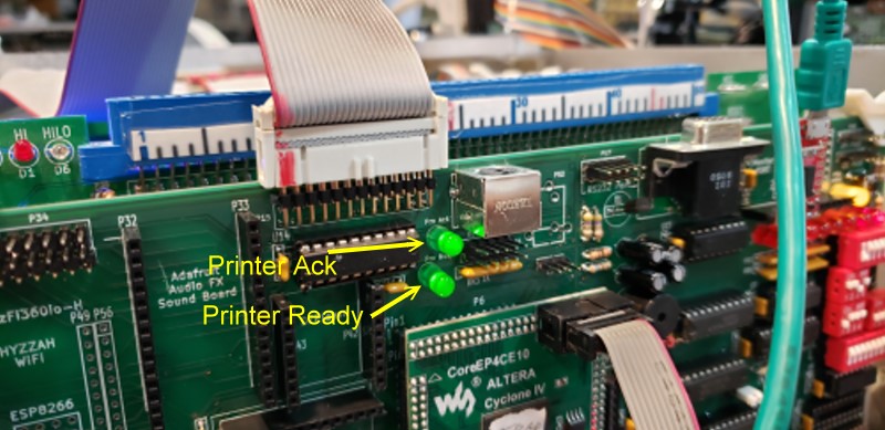
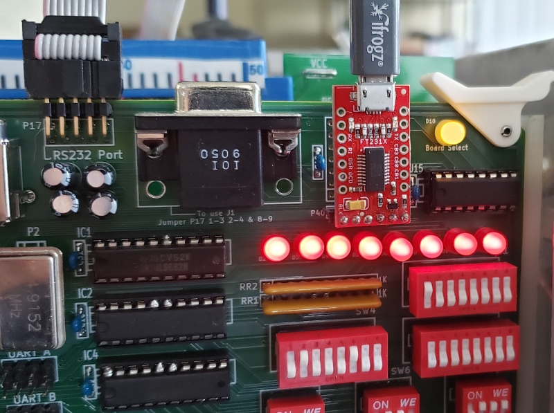
Please note that I have duplicated the 8 printer port pins (p32) along side the Adafruit FX Sound Board P33 header. With jumpers you can program the sound output as described by Adafruit. 
Just send/set bits on the printer port (without sending the printer strobe pulse).   
Please study the schematic to see how outputs from this module are connected.

  
    FX Module on Board

You can add headphones directly through its top socket. Or you can add a speaker via Jumper P48.
Click sample.ogg to hear what the file sample.ogg should sound like on this device.


The
DFRobot MP3 Player
  
    DF Player DFRobot2
 
This is another powerful module in a small package.  Again you need to study the manual before using the module.  The manual can be found here.
The module can be used as a stand alone circuit and has numerous RX/TX capabilities.
It supports sampling rates of (kHz): 8/11.025/12/16/22.05/24/32/44.1/48and and has a  24 -bit DAC output, supports a dynamic range 90dB
It fully supports FAT16 and FAT32 file systems, and has maximum support of 32G of the TF card, support 32G of U disk, 64M bytes NORFLASH,  a variety of control modes, I/O control mode, serial mode. It supports up to 100 folders, every folder can hold up to 255 songs, 30 level adjustable volume, 6 -level EQ adjustable .

Insert the module in the sockets
P46 and P47.  Insert headphone/speaker in P48 (or jumper P15 1-2 and 7-8, remove any others). You can also use 1-3 of P52 to connect to a separate speaker.  In order to fully utilize this module you need to study the manual here before going any further.  Please study carefully the schematic to see how outputs from this module are connected.
 
As for the other above modules,  you may find the module fits tight in the board holes without any socket or solder.  The two rows of pins are very slightly too wide to make a tight connection. If you must use a socket use the Jameco female headers #308592 (cut to size) or a 40 DIP pin socket sides (cut to size).

Jumper P15 1-2 and 7-8. Add an earphone/speaker to P52. Launch the Super IO Board Diagnostic Program and open the "
D" sub menu.
Here is how it should appear:
  
   DFP Player Menu

You can have up to 30 "tracks". I have only 3 so far. If you don't hear a sound trying increasing the volume (~15 is best).
You communicate with this module over a serial line at 9600 Baud. All commands are sent in an 8 byte string.
I have file "01" set as a sound of somebody knocking on a door.
  
Here is a list of some of the control commands. There are others for query of the device.
    
  DFP Commands
 
The DF Player manual describes in detail how to interface with this device.


The ESP-8266 WiFi Module
 
    ESP-8266
   

The ESP8266 processor from Espressif is an 80 MHz microcontroller with a full WiFi front-end (both as client and access point) and TCP/IP stack with DNS support as well.

While this chip has been very popular, its also been very difficult to use.   It absolutely will not tolerate voltages above 3.3v.


Almost endless descriptions of this module exist on the web.  I have described if in fair detail for the original FPGA driven Super IO board.


Suffice to say we need to change the power-up baud rate on this unit using a ESP8266->USB adaptor.  (The are many).
  
    ESP8266-USB Adaptor

You will also need a program like PuTTY to interface/program it (see the bottom of this page for a download).
Initially you will need to configure PuTTY for Serial, 115,200 baud and the correct PC COM port to talk to it from your PC.
Then carefully enter:-
AT+UART_DEF=9600,8,1,0,0
then CR, then Control J (LF).

Reload the PuTTY program and this time configure it to 9600 baud (and the COM port).
The ESP8266 should signon with Ready.
It should also respond to "AT" commands:-
   
    AT Command
You now have the ESP8266 configured to work at 9600 Baud.  You can insert it into the Super IO Board P10 socket.

I have some example software in the SIODIAG2.ASM program (use the "W" menu option). 
You will see for example "AT+CWLAP" returns all the local WiFi networks:-


   WiFi Menu
   
Unlike the other sound modules I like to have this module somewhat above the board surface so it can get a better WiFi signal.
   
   ESP8266-2
 
BTW the blue SMD LED on the ESP8266 module itself should flash twice each time with an S100 bus reset.

  
The 555 Timer

I have also added a simple 555 based variable pulse generator to the board. The circuit is from the SMB.
The pulse goes to directly to the S100 bus vector interrupt pins. The variable cap C14 adjusts the speed of the pulse. Use the 555 for longer pulses (~0.1 seconds).
   
    555 Circuit

Here is a picture of the completed working board:
   
    Working Board


Initilizing the Zilog 85C30 UARTs
The Zilog UARTs are extremly capable and flexable chips.  There is almost no serial protocol they cannot handle.
Unlike older UARTs they have only 4 IO Ports for two (A&B) independent serial interfaces per chip. 
One each 'control' port configures the 'data' port with over a dozen paramaters.  They are generally sent from a table of values.
Here is the code to setup the A port of UART A.

INIT$SCC$A$A:
         MVI    A,ACTL            ;Program Channel A of UART_A
         MOV    C,A
         MVI    B,0EH             ;Byte count for OTIR below
         LXI    H,SCCINIT$A$A
         OUTIR                    ;Z80 Block output to a port
         RET

SCCINIT$A$A:
         DB 04H                    ;Point to WR4 >>>>>>>>>>>>>>>>>>>>> (RS232 UART)
         DB 44H                    ;X16 clock,1 Stop,NP
         DB 03H                    ;Point to WR3
         DB 0C1H                   ;Enable reciever, Auto Enable, Recieve 8 bits
         DB 05H                    ;Point to WR5
         DB 0EAH                   ;Enable, Transmit 8 bits
         DB 0BH                    ;Set RTS,DTR, Enable. Point to WR11
         DB 56H                    ;Recieve/transmit clock = BRG

         DB 0CH                    ;Point to WR12
;        DB 40H                    ;Low Byte 2400 Baud
;        DB 1EH                    ;Low Byte 4800 Baud
;        DB 0EH                    ;Low Byte 9600 Baud
;        DB 06H                    ;Low byte 19,200 Baud
         DB 02H                    ;Low byte 38,400 Baud <<<<<<<<<<< XModem I/O
         DB 0DH                    ;Point to WR13
         DB 00H                    ;High byte for Baud
         DB 0EH                    ;Point to WR14
         DB 01H                    ;Use 4.9152 MHz Clock.  enable BRG
         DB 0FH                    ;Point to WR15
         DB 00H                    ;Generate Int with CTS going high

This code can be easily incoportated into any program.

The actual handling of port data looks like this:-

USB$OUT:                                                       ;Send Data
                 XRA     A                                        ;Will try 256 times, then timeout
USBXXX:    PUSH   PSW
                IN        USB$STATUS$PORT             ;SERIAL OUT
                ANI      04H                                    ;Are we ready for a character
                JNZ      USB$SENDM                        ;NZ if ready to recieve character
                POP     PSW
                DCR     A
                JNZ      USBXXX
                RET
USB$SENDM:
                POP     PSW
                MOV     A,C
                OUT     USB$DATA$PORT                  ;Send it
                RET


USB$IN:                                                           ;Get Data
                 IN        USB$STATUS$PORT             ;U10 B status port
                 ANI     01H
                 JZ       USB$IN
                 IN       USB$DATA$PORT
                 RET

USB$STAT:                                                     ;Get Serial Input port Status
                 IN         USB$STATUS$PORT           ;U12 B status port
                ANI        01H
                 RZ                                                 ;Ret NZ if nothing
                XRA        A
                DCR        A
                RET                                                ;Ret FF/NZ if something


Switches

The board has a number of dip switches to set IO port addresses.  They are in blocks of 4 or 8 ports.  Please study the schematic to understand how each "block" of ports are assigned.
  
         Switches
  
The default port addresses used by the SIODIAG2.ASM software is as follows.

UART A, U7    RS232 Port  89H & 8BH    Speech    88H & 8AH       
UART B, U8    FX Audio    9DH & 9FH    DFP Audio 9CH & 9EH 
UART C, U10   WiFi        8DH & 8FH    USB Port  8CH & 8EH 

8255A   U9           5CH-5FH
8255A   U13          3CH-3FH

Remember you can check each port address by inputting that port from your monitor and looking for a pulse at the chip select pin on the UART or 8255A.
    
BUGS.
No hardware bugs noted so far.  Remember to use Zilog 85C30 UARTS. 
The headphone jack is missing from the BOM. One example is Mouser Part Number 161-379XS-L. (Thanks Peter Higgins).
 

To Order a Production S-100 Board
A number of people may want to utilize a board like this.  Together with a group of people on the  Google Groups S100Computers Forum, a "group purchases" has been setup on that forum.

If you would like a bare board please apply from there.


Please note some of the above pictures of the boards during the build process are late stage prototypes. The position of certain items may be slightly changed from the final (V1.0) versions.


The links below will contain the most recent schematic of the above boards.
Note, it may change over time and some IC part or pin numbers may not correlate exactly with the text in the article above.

Super IO Board II Schematic FINAL            .PDF File  (08/11/2022)
KiCAD files for Super IO Board II FINAL     .ZIP File     (08/11/2022)
Gerber files for Super IO Board II FINAL     .ZIP File     (08/112022)

 
BOM of Super IO Board (.PDF File)                    (9/18/2022)    Supplied by    Rick Bromagem                            
BOM of Super IO Board  (Excel File)                  (9/18/2022)       Supplied by    Rick Bromagem                              
Super IO Board layout (.PDF File)                      (9/18/2022)     Supplied by    Rick Bromagem                                                  

SIODIAG2.ASM (Text file)                            (10/19/2023)
SIODIAG.ZIP (zip file)                                 (10/19/2023)


Other pages describing my S-100 hardware and software.
Please click here  to continue...


This page was last modified on 10/19/2023