S100 Computers

HomeS-100 Boards HistoryNew BoardsSoftwareBoards For Sale
ForumOther Web SitesNewsIndex  

The 68030 S100 Bus CPU Board.
  
  68030 CPU board
    
In 1976, designers at Motorola began working on a 16-bit microprocessor to compete with the Intel 8086 CPU.  Their focus was software more than hardware. The wanted to have a CPU with internal 32 bit registers and an external 16 bit interface.  Unlike Intel, they wanted to eliminate any special-purpose instructions and allow the microprocessor to perform all operations, on all registers, on all data types, and in all addressing modes.  Assembly language programmers like this because it means they don't have to memorize a bunch of exceptions to the instruction set.  However this advantage was limited because the bulk of code programming even at that time,  was above this level of detail.  That said, the 68000 leant itself to UNIX style  systems. There were a number 16 bit 68K CPUs, but none really became successful like the Intel 16 bit CPUs.  If it were not for the Apple Macintosh,  the 68000 CPU would have probably have ended up like some of its relatives, the Zilog 8000 or National 16032.

The 68000 could address 16 MB of physical memory with byte resolution. Address storage and computation used 32 bits, however, with the high-order bytes were ignored due to the physical lack of pins. This allowed it to run software written for a flat 32-bit address space. Motorola's intent with the internal 32-bit address space was forward compatibility, making it feasible to write 68000 software that would take full advantage of later 32-bit implementations of the 68000 instruction set. 

This happened in 1984 when Motorola came out with its full 32-bit extension to the 68000, the 68020. Initial clock speeds were 12 MHz but this later went up to 33MHz.  It had one neat feature, you could dynamically choose the bus size you want  8, 16, or 32 bits with two external pins on the chip.   This for example allowed you to use a single boot ROM instead or 2 (or 4) as was the case in the with 16 bit wide systems.  They also picked up on the Intel idea of bus buffering by using an efficient "cache". The cache in the 68020 was 256 bytes deep and works a little differently from the 8086 queue. If a jump occurs to a point outside the queue, the queue was flushed and reloaded. But the cache looks just like memory, so a jump to a point in the cache would not cause the cache to be dumped and re­loaded. If loops are small enough, they can execute directly from the cache.
  

There was 68010 but it was really a patched bug repaired version of the 68000 that was supposed to work with Motorola's memory management chip (68451). Suffice to say there were problems.

The 68020 added many improvements to the 68000 including a 32-bit external data bus and address bus, and a number of new instructions and addressing modes.  There were also some minor improvements and extensions to the supervisor state.  The 68020 had a coprocessor interface to incorporated a paged memory management unit (MC68851 PMMU) or a floating point unit (MC68881 or MC68882 FPU) . There was the capability to do bigger multiply (32×32→64 bits) and divide (64÷32→32 bits quotient and 32 bits remainder) instructions, and bit field manipulations were improved.

Unlike its 8086 cousins the 68000 could only access word (16 bit) and long word (32 bit) data if they were word-aligned. The 68020 finally had no alignment restrictions on data access. However, unaligned long word accesses were often much slower than aligned accesses,  as was the case for the 8086.

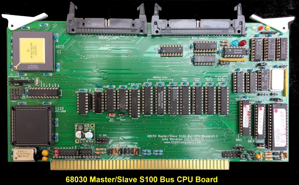
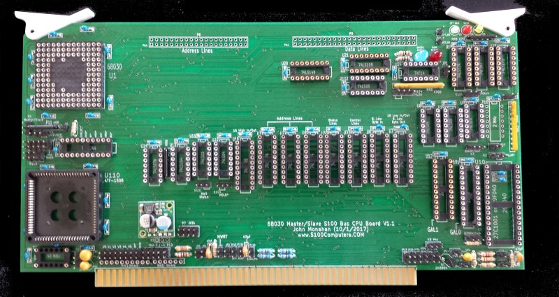
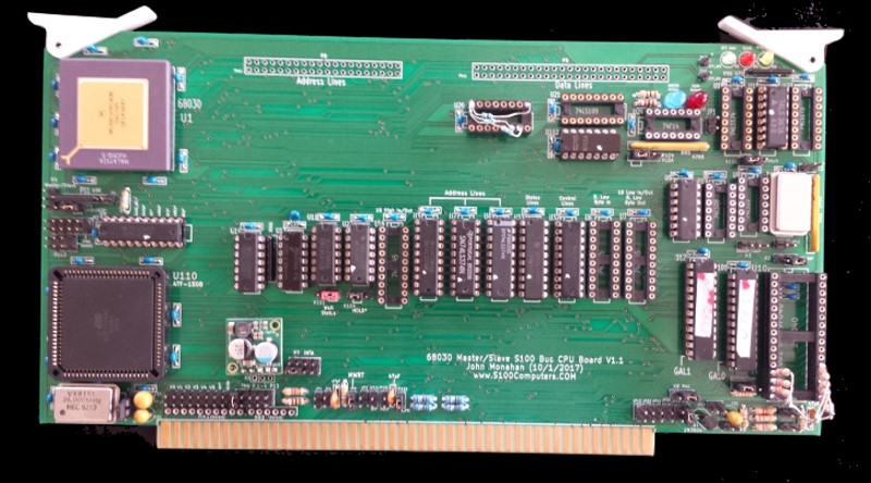
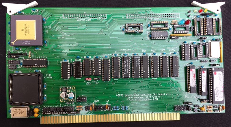
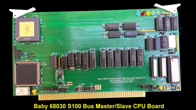
The 68030 was released in 1987.  It had an on-chip memory management unit  (but still  did not have a built in  floating point unit).  This was added with the 68040 which was released in 1990.  It could only reach a speed of 40 MHz because of severe heating problems.  Unfortunately the 68040 did not have 8 bit bus capability.  The 68020, 30's and 40's  were all used in the Apple Macintosh II and later PC lines as well as Sun 3 workstations.

The 68030 was the last 68xxx CPU to have 8,16 or 32 bit dynamic range bus addressing capability.   For this reason we will go with a 68030 CPU board.

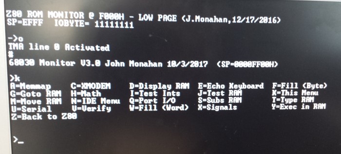
From the assembly language programmers point of view the 68030 is a real joy to program.  Upon power up you immediately have use of all the 32 bit registers and a continuous memory plane of 4GB starting from 0H in RAM.  All the registers are symmetric with no "special cases". 

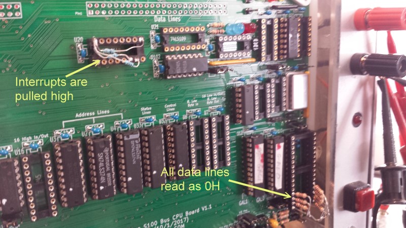
I should point out also that typically when I start a completely new S100 CPU board I anticipate many hardware problems.  The 80386/80486 boards took over a dozen prototypes to get working fast and reliable and almost a year of work.  Admittedly I had that knowledge and experience beforehand with this board, but only 3 prototypes were required -- and two of these were obvious errors on my part. 

As for our 80386/80486 CPU boards we will use the same format of using a single 1508 CPLD to convert the Motorola CPU signals into an S100 bus format.  As before we will use one optional 22V10 GAL to switch the bus Master/Slave configuration and another to identify where the OTT RAM is located in the 4 GB address space.

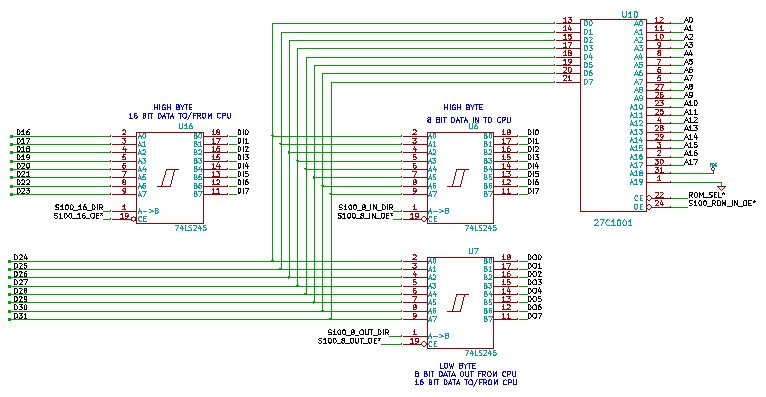
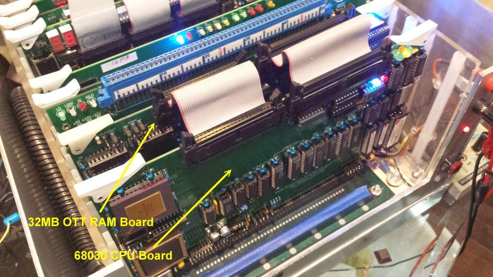
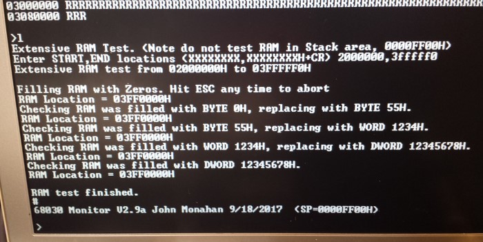
The board follows our 80386/80486 board format with the OTT connectors to allow it to address up to 4GB of RAM. The onboard EEPROM contains the 68030 monitor (see below).  It runs at 9 MHz on the S100 bus in 8 & 16 bit modes and in 32 bit mode when addressing RAM on the OTT bus.  The board works without any changes to our OTT 32/64MB RAM boards that we developed for the 80386/80486 CPUs.    Also because of the much simpler RAM interface with this CPU it was not necessary to go to a 4 layer Full Size 68030 board -- as we had to do for the 80486 CPU board.  There is a jumper option (K7) to use a Flash RAM (29F040) instead of an EEPROM. I will use the EEPROM here.

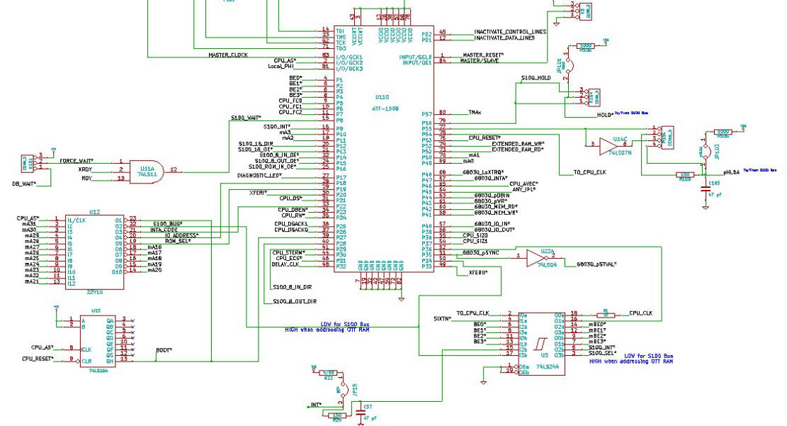
Almost all the above capabilities are programmed into the onboard Atmel 1508 CPLD.   Let us step through the various functions/code this CPLD supplies.


GAL0 Signals.
The current software assumes this 68030 board will act as an S100 bus slave. Later if needed, it can be modified/jumpered as being a bus master.
In hardware, one of the TMA lines (Jumper P13) goes low to start the S100 bus master/slave transfer process.
Just as for the 80486 board, sequentially XFERI & XFERII are then activated (and the S100 bus clock signal PHI, then originates from this board).

Pinnode = [reg2..0];                       /* Need 3 D type Flip Flops */
Pinnode = BOARD_ACTIVE;                    /* BOARD_ACTIVE HIGH if 68030 has control of the bus, see below */

reg0.d = TMAx;                             /* TMAx goes low-> high */
reg0.ckmux = !PHI;
reg0.ar = !MASTER_RESET;                   /* Return to high on reset */
!HOLD = reg0;                              /* Lower S100 bus HOLD line */


!XFERI = reg0 & pHLDA;                     /* Activate the S100 bus Control lines, when pHLDA comes back */

reg1.d = reg0;
reg1.ck = pHLDA;                           /* S100 bus grants bus by raising pHLDA line */
reg1.ar = !reg0;

BOARD_ACTIVE = reg1;                       /* HIGH when bus control comes to this 68030 Board */
!XFERII = reg1;                            /* LOW to activate S100 bus Status, Data & Address lines */

reg2.d = reg1;
reg2.ckmux = !PHI;
reg2.ar = !reg1;


CPU_RESET = reg2;                          /* Activate the CPU, Raise it's reset pin */


This is the same approach we have used time and time again on all our S100 bus master/slave CPU boards.  TMAx is the key signal that is either generated in "GAL0" (or generated on our SMB board) that pulls one of the S100 Bus TMA lines low thereby triggering a master/slave switch.  This process is define in the S100 bus IEEE-696 protocol.
 

GAL1 Signals.
For this 68030 board the CPU will be talking to two completely separate RAM circuits. For RAM below 16MB it will address RAM on the S100 bus. Any RAM above this address space will be assumed to be on the extended OTT bus using the overhead connectors. All port I/O's and Interrupts will also be on the S100 bus.  The relevant signal that defines which bus the CPU is talking to is the
S100_BUS signal. If it is low the S100 bus is being addressed. If it is high the "over the top (OTT) bus" is being addressed.  So within the 4GB address OTT RAM range (S100_Bus HIGH), any RAM being addressed will require S100_BUS to be high. The default is a 32MB board at 2000000H to 3FFFFFFH.  This value is programmed into the "GAL1" 22V10 GAL pin 22.

Unlike the Intel CPU family the Motorola CPU's do not have dedicated port I/O pins or software.  Ports in Motorola hardware are defined as specific memory locations.  They can in theory,  be anywhere,  but its usually best to keep them out of the way of your software code.  For our 68000 CPU board and 68K monitor we located all S100 bus I/O ports at 00FF0000H to 00FFFFFFH.  For this 68030 CPU board we will locate all S100 bus I/O ports at FFFF0000H to FFFFFFFFH.  Again within the "GAL1" 22V10 GAL any CPU address within this range will arrive at the 1508 CPLD (pin 29), as "
IO_ADDRESS".   Code (see below) within the CPLD will then translate the CPU RAM addressing to S100 bus port addressing.

As we will see below,  the 68040 puts out a special code on the ADDRESS lines when it is acknowledging an interrupt.  This code resides in the address lines A16 to A19.  During an interrupt acknowledge sequence they are all
1's.  We use our GAL1 again to recognize this value. When true (INTA_CODE*) is low on pin 21.

We are almost there, there is one final complication is splicing the 68030 on to the S100 bus.    As with all the previous Motorola 68K CPUs upon power up the CPU ALWAYS reads the first 4 bytes of RAM and uses it as its stack pointer. It then reads the next 4 bytes of RAM as the location where it will immediately jump to begin processing.   The latter can be any place in its 4GB address space.  This process always occurs -- no exceptions.

Now normally you don't want a ROM at 0H in RAM.  We use a hardware trick to temporally activate the ROM for only the CPU's first 8 read cycles after power up and after that in affect, relocate the ROM to high memory.  The default high memory location for this board is 00FC0000H.  Low RAM is unaffected and available (even 0H-7H). This cleaver trick was described by Alan Wilcox in his book for the 68K CPU.  In the schematic (see below) U13 and "GAL1" generates the
ROM_SEL* signal that allows the ROM to appear on the S100 bus.  ROM_SEL* goes to the CE pin 22 of U10 a 128x8K 271001 EEPROM.

All of the above critical signals are generated in the "GAL1" GAL.  The inputs are the CPU address lines latched by the CPU AS* signal.  Here is the relevant GAL code:-

!IO_PORTS = mA31 & mA30 & mA29 & mA28 & mA27 & mA26 & mA25 & mA24               /* S100 Bus up to 16MB Only */
          & mA23 & mA22 & mA21 & mA20 & mA19 & mA18 & mA17 & mA16;              /* Ports at (FF)FFxxxx */

IO_PORTS.ar = 'b'0;
IO_PORTS.sp = 'b'0;

!ROM_SEL = (!BOOT                                                               /* ROM for first 8 cycles */
         # (!mA31 & !mA30 & !mA29 & !mA28 & !mA27 & !mA26 & !mA25 & !mA24
         &   mA23 & mA22 & mA21 & mA20 & mA19 & mA18 & !mA17 & !mA16));         /* for ROM at (00)FCxxxx */

ROM_SEL.ar = 'b'0;
ROM_SEL.sp = 'b'0;


!S100_BUS = ((!mA31 & !mA30 & !mA29 & !mA28 & !mA27 & !mA26 & !mA25 & !mA24)    /* If RAM address is < 16M */
           # (!IO_PORTS));                                                      /* and I/O at FFFFxxxx */

S100_BUS.ar = 'b'0;
S100_BUS.sp = 'b'0;


!INTA_CODE = mA16 & mA17 & mA18 & mA19;             /* When FC0,FC1 & FC2 = 111 & A16,A17 ,A18 7 A19 = 1111 */

INTA_CODE.ar = 'b'0;
INTA_CODE.sp = 'b'0;


CPLD Signals.
Synthesize the S100 Bus Control and Status signals
This is the very heart of the board. Just as for the 80486, we need to carefully reformulate the main 68030 control signals to their S100 bus counterparts. Unlike the 80386/80486 signals I found that it was not necessary to modify or shorten the length of some of the 68030 signals to have them conform/work with our S100 bus RAM or I/O boards.  In fact all in all, I found the signal conversion process was simple and easy for this CPU.  Here is the relevant CPLD code.

!MEM_WR = !CPU_RW & !CPU_DBEN & BOARD_ACTIVE & IO_ADDRESS & !S100_BUS;             /* CPU_RW, remember inverted by U33. */

!MEM_RD = CPU_RW & !CPU_DBEN & BOARD_ACTIVE & IO_ADDRESS & ROM_SEL & !S100_BUS;    /* RAM,  so IO_ADDRESS will be HIGH */

!IO_OUT = !CPU_RW & !CPU_DBEN & BOARD_ACTIVE & !IO_ADDRESS & !S100_BUS;            /* Ports IO_ADDRESS will be LOW */

!IO_IN = CPU_RW & !CPU_DBEN & BOARD_ACTIVE & !IO_ADDRESS & !S100_BUS;

ssWO = !CPU_RW & !CPU_DS & BOARD_ACTIVE & !S100_BUS;                                /* RAM or I/O Write, (inverted) */

!INTA = !INTA_CODE & CPU_FC0 & CPU_FC1 & CPU_FC2 & !CPU_AS;

pSYNC_68K = CPU_AS & !CPU_ECS;

ppDBIN = !CPU_DS & CPU_RW & BOARD_ACTIVE & !S100_BUS;                               /* pDBIN is active HIGH on S100 bus */

!dpWR = !CPU_DS & !CPU_RW & BOARD_ACTIVE & !S100_BUS;                               /* pWR* is active LOW on S100 bus */


!S100_8_IN_OE = CPU_RW & !CPU_DBEN & sXTRQ & BOARD_ACTIVE & ROM_SEL & !S100_BUS;    /* 8 Bit Data S100 bus Read */

!S100_8_OUT_OE = ((!CPU_RW & !CPU_DBEN & sXTRQ & BOARD_ACTIVE & !S100_BUS)          /* 8 Bit Data S100 bus Write */
               # (!CPU_DBEN & !sXTRQ & BOARD_ACTIVE & !S100_BUS));                 /* 16 Bit Data S100 bus LOW byte R/W */


!S100_8_IN_DIR = CPU_RW & sXTRQ;
S100_8_OUT_DIR = !CPU_RW;                                                           /* Use for both 8 & 16 bit data */

S100_16_DIR = !CPU_RW;                                                              /* Use for both 8 & 16 bit data */
!S100_16_OE = !CPU_DBEN & !sXTRQ & BOARD_ACTIVE & ROM_SEL & !S100_BUS;              /* 16 Bit Data S100 bus HIGH byte R/W */


!S100_ROM_IN_OE = !CPU_DBEN & CPU_RW & BOARD_ACTIVE & !ROM_SEL & !S100_BUS;         /* Read Onboard ROM, LOW at 00FC0000H */

Unlike the complex data bus buffer arrangement we had for the 80386/80486 CPU boards, this board only requires three 74LS245s to interface with the S100 bus.  In fact if the CPU is configured for 8 bit mode (see below) only two (U6 & U7) are required.  Here is a schematic of these buffers.
      
IO_Buffers
    
The 74LS245 is  a bidirectional buffer, the direction being set by its pin 1.   This is provided (via the CPLD), by the CPU_RW signal on the CPU (pin L3).  On the S100 bus,  8 bit data is handled on two 8 bit data lines. One data into the CPU (U6) the other data from the CPU (U7).  For such transfers the S100 bus status pin sXTRQ is high.  Any time 16 bit data is being processed by the CPU the sXTRQ line (S100 bus pin 58) is low.  In this situation the above data in and data out lines are converted into a bidirectional 16 bit data bus.  The above code activates the appropriate 74LS245 OE pins of U16 and U7.

Finally in the special case when the CPU is reading the 8 bit wide ROM code all 3 of the above buffers are inactivated (ROM_SEL is low),  and the 8 data bits flow directly to the CPU D24-D31 data lines.   Working with the 80486 you might expect 8 bit data to flow into the CPU D0-D7 data lines.  However the Motorola chip utilizes a "big-endian format".

We now get to the complicated aspect of dynamic data bus sizing.  The 68030 can work with an external 8, 16 or 32 bit wide data bus.  For every data cycle we need to let the CPU know what width data bus it can expect.  This is done by providing High/Low inputs to two pins on the CPU, DSACK0 and DSACK1.  The CPU interprets this data as follows.
  
 DSACK1DSACK0                     Status
 HIGH HIGH   Place wait states on CPU
  LOW LOW  A 32  bit Data is bus available
  LOWHIGH   A 16 bit Data bus is available
  HIGH LOW  Only an 8 bit Data bus is available
  
The DSACK0 and DSACK1 signals and the S100 bus sXTRQ signal is generate in the CPLD then as follows.

!CPU_DSACK1 = ((S100_BUS & S100_WAIT)                      /* Always 32 bit Transfer for OTT RAM */
            # (!sXTRQ & S100_WAIT & !S100_BUS));           /* 16 bit Transfer for S100 bus RAM */

!CPU_DSACK0 = ((S100_BUS & S100_WAIT)                      /* Always 32 bit Transfers for OTT RAM */
             # (sXTRQ & S100_WAIT & !S100_BUS));           /* 8 bit Transfer for S100 bus RAM */


!sXTRQ = CPU_SIZ1 & !CPU_SIZ0 & !mA1 & !mA0 & BOARD_ACTIVE & ROM_SEL & IO_ADDRESS;

You may note above that the only time a 32 bit data bus is acknowledged is if S100_BUS is HIGH -- when the OTT RAM is being addressed.

The 32/64MG OTT RAM board is described in detail here.  Essentially the 32 bit bus is divided into four 8 bit wide data banks.  These are individually addressed by the signals BE0*, BE1*, BE2 & BE3*.  How the CPU addresses any of these banks either individually, or as 2, 3 or 4 banks together is quite complex.  In fact unlike the earlier CPUs this CPU can address a bank on any byte boundary.  Fortunately Motorola provides code to program a GAL to handle all this in the 68030 manual.    I have incorporated this code in our CPLD as follows.

!BE3 = !mA1 & !mA0 & !CPU_AS;

!BE2 = ((!mA1 & mA0 & !CPU_AS)
      # (CPU_SIZ1 & !mA1 & !CPU_AS)
      # (!CPU_SIZ0 & !mA1 & !CPU_AS));

!BE1 = ((mA1 & !mA0 & !CPU_AS)
      # (!CPU_SIZ1 & !CPU_SIZ0 & !mA1 & !CPU_AS)
      # ( CPU_SIZ1 & CPU_SIZ0 & !mA1 & !CPU_AS)
      # (!CPU_SIZ0 & !mA1 & mA0 & !CPU_AS));

!BE0 = ((mA1 & mA0 & !CPU_AS)
      # ( CPU_SIZ1 & CPU_SIZ0 & mA0 & !CPU_AS)
      # (!CPU_SIZ1 & !CPU_SIZ0 & !CPU_AS)
      # ( CPU_SIZ1 & mA1 & !CPU_AS));

!EXTENDED_RAM_RD = CPU_RW & !CPU_DBEN & BOARD_ACTIVE & IO_ADDRESS & S100_BUS & OTT_RAM_WINDOW;
!EXTENDED_RAM_WR = !CPU_RW & !CPU_DBEN & BOARD_ACTIVE & IO_ADDRESS & S100_BUS & OTT_RAM_WINDOW;

The two CPU signals CPU_SIZ1 and CPU_SIZ0  originate from the CPU.  They indicate the number of bytes the CPU is in the processes of sending during each data cycle
.
  
 SIZ1SIZ0            SIZE
 LOW HIGH   BYTE
  HIGH LOW  WORD
  HIGHHIGH   3 BYTES
  LOW LOW  LONG WORD
  
The two signals EXTENDED_RAM_RD and EXTENDED_RAM_WR are the key Rad/Write signals to the actual RAM chips on the RAM board.  Clearly they are only active when the S100_BUS is high and the OTT RAM window is actually present within the total 4GB CPU addressing domain.

For the actual 1508 CPLD every one of its I/O pins are utilized.   Here is a schematic.
 
 CPLD Schematic

This is the very heart of the board.  Because essentially all the CPU signals go through this CPLD to the S100 bus the board lends itself well to future modifications and tweaking.  Again unlike the 80486 CPLD the code for this CPU is dirt simple -- a real joy to do in fact.   Within the 68030 monitor (see below) is an extensive RAM test.  With all our S100Computers RAM boards the CPU ran fine with a 9 MHz PHI bus signal (a 36 MHz Oscillator).   I have not tested it with other S100 bus RAM boards.  If you are using old S100 bus 64K etc. boards,  be sure you adjust the stack value. Non IEEE 696 boards will probably not run at anything close to 9MHz. The CPLD code may have to be modified to run the CPU in 8 bit mode (
sXTRQ = 'b'1;).   It is recommended you use at least a 4MB RAM board, ideally the 16MB RAM Board.


Interrupts
The one fly in the ointment with putting the 68030 CPU on the S100 bus is the handling of interrupts.  The 68030 (and in general the 68K family) handles external hardware interrupts quite different from say the Intel 86 family of CPU's.  They are handled in two different ways. 

In the first approach, when the 68030 processes an interrupt, it performs an interrupt acknowledge cycle to obtain from the data bus, the number of the vector that contains the starting location of the interrupt service routine.  It expects that vector to be on its data bus when the following situation is setup.

1    The CPU output pins FC0-FC2 are set to
111.
2.   The address lines
A1, A2, and A3 are set to the interrupt request level (the inverted values of IPL0, IPL1, and IPL2, respectively, see below).
3.   The CPU address lines A16-A19 are set to
1111 (the interrupt acknowledge code).
4.   Also the CPU address lines A20-A31, A4-A15, and A0 are set to 1.

The interrupt device places the vector number on the data bus when the above conditions are met.   There is no equivalent of the Intel 8259A which places a vector on the bus no matter what,  simply after receiving two INTA pulses.  If you wish to utilize this approach your interrupting device must be built around the above conditions.

The second approach is much simpler.  It utilizes an "Autovector Interrupt" approach.  It is used when the interrupting device cannot supply a vector number as described above.  Instead of placing a vector number on the data bus, the device lowers one or more of the three 68030
IPL0, IPL1 and IPL2 lines.  It then lowers the CPU  autovector signal AVEC* (via ANY_IPL* to the CPLD and out via CPU_AVAC*) .   This causes the CPU to terminate the current cycle and process the interrupt.   The 68030 ignores the state of the data bus and internally generates the vector number. It is always the sum of the interrupt level +18H. There are seven distinct autovectors that can be used, corresponding to the seven levels of interrupt available with signals IPL0-1PL2.   Note it is up to external hardware to priories the required interrupt and to recognize when it is completed.  This approach in fact is somewhat similar to what we have with our PDP11 CPU board.  Because the CPLD also reads the A1,A2 & A3 address lines, you can determine the IPL0-IPL2 level (they are the inverted values of A1-A3) and in fact repritorize the interrupts if you like.

The problem we run into with our S100 bus is the generation of the INTA signal. This is the S100 bus signal that tells S100 bus boards that an interrupt has been acknowledged by the (current) bus master.  We cannot use the Intel 8259A Interrupt controller on our MSDOS Support board because it requires two back to back INTA signals before it places the highest priority interrupt vector on the S100 bus data lines.  If you wish to utilize an 8259A with this board you will have to generate two back to back INTA S100 bus signals while holding the CPU in a wait state. I have not explored this but I think it is doable with code in the CPLD.   Another approach would be to utilize a more programmable interrupt controller such as the AMD 9519 on a custom board.  For those that want to tackle this approach described above I have placed jumper options to utilize the unused S100 bus lines RFU1-4 and NDEF2.  (Jumper block P7) so you can bring your own dedicated 68030 "INTA" line to your custom board.

The simplest approach is to just use S100 bus interrupts with the CPU autovector option.  I demonstrate this in our 68030 monitor (see below) where we utilize a keyboard input to interrupt the CPU.  In this approach we use the Console IO board keyboard key pressed interrupt (VI1*) to trigger an interrupt.  That board will pull the interrupt line any time you press a keyboard key.  It's actually setup to work in conjunction with the Intel 8259A.  Normally when that chip sees INT V1 pulse low  it will issue a bus Interrupt (INT* S100 bus pin 73) -- if the 8259A is activated.  This is for the Intel word.  Here we have to generate our own equivalent to INT*.  It is
ANY_IPL* from U20 going to the CPLD and then being delivered to the CPU as CPU_AVEC*.  Again within the CPLD there is ample opportunity to modify the process.


Step By Step Building the 68030 CPU  Board
The build instructions are fairly simple for this board but because it is a complex board building it should not be rushed.  First examine the bare board carefully for scratches or damaged traces, use a magnifying glass if need be.  A broken trace is almost impossible to detect by eye on a completed board. Build the board up in functional steps. Avoid the temptation of adding everything at once and popping it into your S-100 box. Step by step is faster in the end -- trust me.
 
I like to run a file at a 45 degree angle a few time at the bottom of the board (both sides) to ease the insertion of the board into the S100 bus. A few strokes is all that is needed.  For some motherboard connectors it may also require a few swipes on both sides of the 100 pin connector area.  Some of the these motherboard 100 connectors are very tight and make the board difficult to remove even with the ejectors.  While I'm on this,  what I did with my "main test socket" in my 10 slot test S100 box is actually use a Damien drill to slightly widen the ends of the socket on both sides.  Be careful not to touch pins 1,50,51 or 100.   This is only for somebody with a steady hand!

We will set the board up as a true S100 bus slave.  By programming the CPLD and with the additional circuitry on the board it can in fact run as a bus master.  I will leave this arrangement to our more experienced users.  Here is a picture of the bare board:-         
 Bare 68030 Board
    
Solder in all the required IC sockets, resistors, the transistor Q1, resistor arrays, capacitors, jumpers, and the 5V voltage regulator.  You can use more modern switcher regulators such as the Pololu # 2850 (5V, 2.5A) or EzSBC.com # PSU5a (5V 2.5A).  Unfortunately there was no room for the old 7805 type regulators. Do not add the LED's yet. Be sure you put the resistor arrays in with the correct orientation of pin 1. Check their values before soldering (they are difficult to remove).  Be sure and have pin 1 of the CPLD socket on the LHS. For prototype boards I typically use common Aluminum Electrolytic caps. For the final board I use the corresponding Tantalum caps. 

Please note, there is a silkscreen error above U18 on the board.  "RR6" should read "RR4".  (The true RR6 is between U14 & U13).  RR4 is a 470 Ohm resistor network. 
 
For prototype boards I generally use "double swipe" IC sockets. For a critical board like this I prefer to use "Machine Tooled" IC sockets.  However they are more expensive and you have to be particularly careful not to bend the IC pins.  The two clock oscillators can have their own special sockets (e.g. Jameco #133006) but actually I find the "Machine Tooled" IC sockets make a better connection.  I in fact solder the 2MHz oscillator (P7) directly to the board since it will never be changed.

In the normal configuration where the board will be used as a bus slave,  Inline sockets should be uses for RR1 and RR3. The is no need for a resistor network.  Also in the normal configuration P11 (jumpers to some CPU pins), should be an inline socket so a 10K or 4.7K resistor network can pull up pins 2-6. P6 is normally left unconnected. 

I normally don't add the top ribbon connectors until later (see below).
 
Place the board in the bus. Check the voltage to sockets on the board is about 5V by placing the board in your S-100 system using an extender board. With no load you will typically get 5.00V  (+/- 0.2V).  BTW, your system should boot and run correctly with its Z80 master CPU board. If not, you have a serious solder bridge somewhere on the board.  Before you do anything else with a magnifying glass go over every socket on the board and examine for proper solder joints. I like to "reheat" each joint just to be on the safe side. The silk screen/varnish on these boards us quite thick. It's easy not to have a good solder joint for the ground pins.  Double check.   Extra time here will save you hours later. 

Next insert all 5 LED's. Before soldering them in place ground one at a time pins 3,5,7,9 & 11 of U13 to be sure they are all OK.    (I always use a blue LED for D3 "Board Active"  in my systems).  Here is a picture of the board at this stage:-
  
  Step0 
   
   
First we will first construct the basic circuit required for the master/slave S100 bus flip.
Please remember that for 3 or more pin jumpers, pin 1 is always the square pad.  It is not necessary the one on the top, or LHS.  

First insert the CPLD in socket U10 taking care that pin 1 is in the center LHS.  Program this CPLD with the code provided at the bottom of this page.  If you are using a virgin CPLD you probably don't need to program it first,  but to be on the safe side you don't want input/output gate conflicts with a previously programed chip.  With no chips/jumpers on the board this is never an issue. Be sure you plug the CPLD burner into the correct pins.

The Z80 should boot up correctly with the programmed CPLD.
Next add the programmed 22V10 GAL0 (U25).  Again the code is at the bottom of this page.  BTW, this is the same "master/slave" GAL0 we use in all our recent CPU boards (except the PDP11 CPU board). Add the 36MHz Oscillator P5 and the 2MHz Oscillator P19. I normally solder the latter into place instead of using a socket. Add JP8.

Add U101 (GAL0), U102,  U22, U5, U15 and U14.  Jumper P13 1-2 (near regulator),  and K108 1-2,  K104 1-2 (under U22),  P104 1-2  and JP102 (bottom center of board).

In your Z80 monitor "O" command (or however in your system you pass control over to an S100 bus  slave device), check that that pin 12 of U22 goes from LOW to HIGH. With the "O" command  the LED D3 should light up. (The others are undefined). A reset should turn off this LED.
   
Next add U8, U32 & U33.  Add jumper  K2 2-3 (located above the EEPROM).   Unless you are generating MWRT on your front panel (IMSAI etc.), jumper JP9.
Repeat the "O" command and check that pins 1 of U2, U3 & U4 go High to Low. 

We now will insert the 68030 CPU.  We will play a trick on it.  We will set its (8 bit) data bus so it always and only reads 00H for ANY memory address.
The opcode
00H,00H,00H is read as  ORI.B  #0,D0 by the CPU.  So if all the CPU sees are 0's on the bus when the CPU powers on it will continuously cycle its address lines from 0H to FFFFFFFFH. If you have the SMB you should see them increase.  (It may crash when you get to FFFFxxxxH because the S100 bus I/O ports are being addressed).

To accomplish this we need to construct a special "patch" socket that fits into the ROM socket U10. This special socket has its pins 13-15 and 17-21 tied to the ground pin 16 via 1K resistors.  To be safe we will also a similar socket for U20 where its pins 6,7 & 9 are tied high to pin 14.  This is to avoid false interrupts triggering the CPU during this build process.
 
Very carefully insert the CPU.  The pins on these CPUs are actually quite strong but they need to be exactly aligned to fit the special socket for this CPU. I use the trick of straightening them out by placing them one side at a time in an old Pentium socket that has a press leaver.   Be absolutely sure you have no bent pins.  You can look between the CPU and socket easily with a light before pressing in the CPU completely. Also be sure pin one is on the bottom LHS.  
Add U13, U11, U3, U2 and U4. Add GAL1 (U12). Jumper K1 2-3, P7 1-3, K7 1-2, K8  2-3, K7 1-2, K8 2-3, K101 2-3 and K4 2-3. 
Power up the board again.  Here is a picture of the board and "patch" sockets.  
  
  Step1
  Patch Sockets
   
Check that when the CPU powers on it will continuously cycle its address lines from 0H to 00FFFFFFH. If you have the SMB you should see them increase.
Here is a short video showing the Address Lines Roll test in action.


With the each reset/new "O" command check pin 13 of U13 goes from low to high and the "address roll" display continues.  If you have our SMB Board (or Front panel equivalent), and press the "Stop" switch the Hex display should stop. Release the Stop switch and it should continue again.
Do not go further unless these two things happen.

Remove the ROM "Patch Jumpers Socket".  
Next Add U7 and add a programmed 27C1001 ROM (or better, a Greenliant GLS29EE010 EEPROM) with -
              
        ORG $00FC0000

TEST:   DC.L $00008000            ;SSP = 008000H
        DC.L $00FC0008            ;PC = 8H (Next byte)

        ORG $00FC0008

START:  MOVE.B #$34,D0            ;ASCII '4' to D0
        MOVE.L #$FFFF0001,A0      ;Point to hardware Port 01H (CRT, Propeller Console IO Board)
        MOVE.B D0,(A0)
        BRA START

With your PROM burner check the first few bytes of code in the EEPROM are:-

00 00 FC 00 00 FC 00 08 .....

These test programs are available at the bottom of this page. (The above is
IO-Test_A.X68). 
With
the "O" command you should see continuous 4444444... on your console.
If not then reassemble the above at ORG 0H, tie U13 pin 13 high and try at that address.  If that is OK then check U13 pin 13 is going low to high. 
Do not go further unless you get the above test to work.  (You are using the ROM for 8 bit data input and U7 for 8 bit data out).

Next add the data buffers U6 & U16 and 16 bit RAM read and write IO Port functions.  Jumper P7 1-3 (INTA bottom two pins LHS).
IO-Test_B.X68 repeats the above test but this time reads the console status port before outputting a character (5's).
IO-Test_C.X68 repeats the above test but this time reads the console keyboard port and outputs that character to the screen.

Next we will test RAM read/write functions.
With your Z80 fill RAM 0-100H with 0's. Then with the 68030 IO-Test_D.X68 read a keyboard character.  Here is the code:-
  
           
   MOVE.L    #$00000000,A2         ;Write byte to RAM at 0H
         MOVE.B    #$34,D1               ;ASCII character
FILL:    MOVE.B    D1,(A2)
         JMP FILL


Reset, and check RAM location 0H has the value 34H.
If not you have a RAM write problem. Using a logic probe, locate where the signal is missing in the above continuous loop.  Try changing the stack location as well.  If no lights are flashing on your RAM board, chances are you are somehow sending out an S100 bus INTA signal. Check P7.

IO-Test_E.X68
tests RAM read and write. You should see 31H in RAM starting at 0H. If you have our 16MB RAM board only the 8W (D4) should light up

IO-Test_F.X68
is the same test except this time we write and read back words.  If you have our 16MB RAM board only the 16W (D5) should light up.  If this test fails check the sXTRQ* S100 line.   Note the current CPLD code does not check for 8 bit only RAM (SIXTN* not going low).  This can be added if required.

IO-Test_G.X68 tests CPU using the RAM stack. Whatever character you type should appear on the console.

IO-Test_H.X68 is a critical test. This routine repeats the above IO-Test_E byte test as but this time writes and reads are handled using the stack.  The values are also displayed on the console - rechecking I/O.  Here  is a picture of the output you should see:-
  
  Test_H Output
   
Here is a picture of the board at this stage:-
  
  Step2
   
If you get this far you are well on your way to having the board up and running.

Next we will burn the 68030 Monitor, insert the EEPROM and boot the system. 
If you are feeling lucky you can in fact jump directly to here and skip all the above test routines.
If it does not work double back and locate the problem.
 
The monitor (available at the bottom of this page) -- is currently being upgraded -- but it should sign on something like this:-
  
 Signon

Were are almost there.  Next we need to add in the circuit to handle S100 bus interrupts (and a circuit for a setup where the board is a true S100 bus master, and a watchdog timer).  Remove the U20 resistor jumpers and add U20, U21, U18, U23, U19 & U9.  Leave U24 out for the moment. Jumper J1 2-4 (V1*). This is the Console IO board interrupt V1*. 

Boot up the 68030 and activate the menu "I" command. 
The CPU will go into a loop just outputting the '.' character on the screen.  If a keyboard character in entered. It will trigger an interrupts on V1*. With the default CPLD code the diagnostic LED (D5) should flash.

Here is an example of the display:- 
          
  Interrupt test

Note a only a very simple Interrupt handler for V1 has currently been written in the 68030 monitor. Normally you would use this interrupt to place a character in an "In Buffer" in RAM.  By connecting individual pins on the bottom row of J1 to different pins on the top row you can implement 7 different interrupt vectors in RAM. To use and pritorize the 68030 interrupts in software you need to carefully read the Motorola manuals etc.  The hardware is on this board -- you need to implement the software. 

Testing OTT RAM access
The final part of the build process is to implement the OTT RAM interface for this board. The S100 bus section can only utilize 16MB of RAM.  The OTT RAM section can interface (in theory) over 3GB of RAM. Lets get started.

Add U24 and solder in the 40 and 50 pin top connectors.  Try and obtain connectors with the built in ejectors.
Insert the board in the S100 bus system and connect it to our 32/64 MB OTT RAM board as shown here.  Be absolutely sure of the pin 1 position in all 4 sockets and the cable.
Save yourself time in advance by checking with a meter.
 
  With OTT RAM
   
Assuming you are using the 32MB OTT RAM board with a start address of 2000000H, when you run the 68030 monitor "Memmap" command you should see 'R" from 2000000H to 3FFFFFFH. Here is a short video showing the Memory Map command board in action.


The 68030 Onboard Monitor.
I must say I am very impressed with the programming capability of the 68030 chip.  Relative to the 80486 or 68K it is a joy to program.  No special registers, no address line shifting etc. just an immediate full block of 4GB of RAM right from the get go. However you will need to carefully read the 68030 handbook to get familiar with all its programming capabilities. 

There are many good assemblers for the 68000 family of CPU's.  I have been using a fantastic package written some time ago by Tim Larson, Paul McKee and Chuck Kelly called "Easy68K".  It can be downloaded from the bottom of this page.  It runs as its own self contained IDE in windows. Not only does it have a complete assembler but it has a self contained Run and Debug interface.   The only catch is that all console IO goes through the 68k software interrupt Trap #15.  Using this debugger you can quickly write and test code before programming an EEPROM.  The only change being you replace Trap #15 with an output to your Console I/O port. 

My first step was to write a simple 68030 specific ROM monitor.  My goal is to model it after the 80386 monitor I wrote.  I wanted to use all the same menu options -- to keep life simple, and in particular extensive OTT RAM testing. I should point out that there are a number of excellent well tested 68K monitor programs. The Motorola Educational Computer "Tutor" perhaps being the best known.

As a total beginner however, I have found understanding this program a little tricky.  If needed it can be seen here. I have opted to write my own. First to learn 68K assembly programming but perhaps more important it will allow me to more easily later splice in code (as I have in the 8086 monitor) to run diagnostic tests on our IDE and ZFDC controller boards.  This should help a lot getting CPM-68K up and running.

The 68030 monitor program is "a work in progress".  The Windows emulator Easy68K has been very useful in laying its groundwork and initial debugging.  The most up to date versions can be obtained at the bottom of this page. 
   
  Signon
    
Amongst the monitor commands is the "Y" command. This command moves the following code:-

TEST_OTT_RAM:
          MOVE.B     (A0),D5        ;Check CRT status is ready to receive character
          AND.B      #$04,D5
          TST.B      D5
          BEQ        TEST_OTT_RAM
          MOVE.B     #$33,(A1)      ;Output ASCII to hardware port 01H
          BRA        TEST_OTT_RAM


to a user specified location in OTT RAM.  The CPU then jumps to that location and executes the code continuously.  This is the most brutal test of the board because it is rapidly switching between 8 bit S100 bus I/O and the 32 bit OTT RAM.  You should run the test overnight for safety.   Make sure however you place the routine on an even address boundary.  I test my system with a 40MHz Oscillator, no wait states,  on the OTT RAM (4 layer) 32 MB board overnight with no problems. 

In the monitor there is also a basic RAM test ("J" command) to test for "stuck bits" etc.  Here is a display of the output:-
  
  RAM Test
   
See here for more information about this 68030 moniotor


68030 Board Comments
It's interesting to me that whenever I start a new board I usually seem to have a good idea about how difficult it will be to construct and get it working with all our other S100Computers (and other) S100 boards.  Sometimes however I underestimate the difficulties. The 80386/80486 boards being an example of a serious underestimate.  I have to say that getting this 68030 board was way easier than I thought it would be.  I did only 3 prototypes and these were essentially to correct obvious errors on my part.  Considering the power and internal complexity of the 68030,  the board required has far fewer
ICs than any other 16/32 bit CPU we have done.  I actually started off with a "Baby 68030" board along the lines of our Baby 80486 board. See here:-
    
  Baby 68030 CPU Board
    
This board can only address the S100 bus RAM (16MB).  It's rock solid with a 10MHz bus Phi clock.  Notice how few support chips it contains.  I was originally going to supply two versions of the board.  But since the "Full Size" 4GB 32 bit RAM addressing capability essentially only requires the OTT cable connectors and two more IC's I decided to drop that option. 

Relative to a number of other S100Computers boards I think you will find this one somewhat easy to build.  If you take care and burn the CPLD, GALs and ROM it should come up the first time if you have the jumpers correct.  For debugging however I have added a number of very short test routines of increasing complexity to burn into the onboard ROM, see below.  Use these to identify any RAM or port access problem you may have.

   
The 68030 Board Jumper Table
There are a fair number of jumpers on this CPU board and they need to be set carefully.  To run the board as a bus slave (with a Z80 master),  here is a typical jumper setup:-
                
 
Jumper   Function 
JP9Normally closed. Generate the S100 bus MWRT signal on this board when it is active.
JP8Normally closed. Generate the S100 bus 2MHz Clock signal on this board when it is active.
K108For slave mode 1-2
J3Bus error detection. Normally not needed, so open.
JP12, JP13, JP14Normally all open unless the board is a bus master.
P104VIP jumper, for slave mode 1-2
K104VIP jumper, for slave mode 1-2
K101For testing jumper 2-3. Jumper 1-2 with OTT RAM board. If pin 2 is grounded the CPU halts until released.
P11These jumpers are all normally tied high using a 10K Resistor array with pin 1 at VCC. P6 is unused
K6To set Slave/Master mode in CPLD code. Currently not used
JP102Jumper after the CPLD is programmed
K2,JP2,JP4 & JP5These jumpers are only used for a specialized configuration (The 68030 slave calls another slave). Normally only K2 2-3
K3Normally 1-2 to allow NMI interrupts
P2 or P103CPLD JTAG programming socket. For Rockfield Research 1508 programmer use P103. Pin 1 is bottom left.
JP15, JP101,JP103If a bus master use the 1K pull-up. In slave mode open.
JP19,JP20,JP21,JP22In slave mode always open
P13S100 Bus TMA line to activate board. Normally 1-2 (or 3-4) closed.  If used with 80486 use 5-6 etc.
K1Normally both 2-3
K7Onboard 27C1001 EEPROM 1-2, Onboard Flash RAM 29F040 2-3
K8Onboard 27C1001 EEPROM 2-3, Onboard Flash RAM 29F040 1-2
J1Inputs from S100 bus Interrupt vectors.
JP1Connect CPU Clock to OTT RAM board. Normally open.

68030 S100 Board Parts
The 68030 chip is not available from most vendors.  It is found on eBay -- either as the chip alone or it can be pulled from Apple boards.   It is almost always socketed on those boards. A typical eBay price is $100/chip.  While outside the specs in the Motorola manuals,  in 5 out of 5 cases I found the 40MHz chips ran fine at the low speed of 9MHz.  Most of the other components used on this board are common. I usually get them from obtained from Anchor Electronics and Jameco or Mouser.  The CPU socket is a little strange. Again I got mine on eBay.
   
  Sockets

Some (later) versions of the 68030 do not have the pins indicated with the above arrows. These are  CPU 'NC' pins and are the only ones omitted.  Perhaps they were originally intended to prevent miss-clocking of the CPU.  That pattern was asymmetrical so it could only be installed one way. Anyway these CPUs appear to behave the same way.

68030 CPU Board  Bugs & Notes.
Damian Wilde noticed is that when the CPU performs a DWORD read or write, on an even byte boundary, to the S100 bus, it performs 4 eight bit bus cycles not the 2 sixteen bit cycles one would expect.  Similarly when the CPU performs a WORD read or write on an even byte boundary that is not a DWORD boundary, it performs 2 eight bit bus cycles not 1 sixteen bit cycle.
He changed the line of CPLD code that sets the sXTRQ signal from:

!sXTRQ = CPU_SIZ1 & !CPU_SIZ0 & !mA1 & !mA0 & BOARD_ACTIVE & ROM_SEL & IO_ADDRESS ;
To:
!sXTRQ = !CPU_SIZ0 & !mA0 & BOARD_ACTIVE & ROM_SEL & IO_ADDRESS ;

Now sXTRQ is asserted in both these cases and the expected sixteen bit bus cycles are executed with no errors running CPM-68K on our 16K RAM board.
Please update your CPLD on the board with the
68030_NEW.ZIP file from below.

In all of the discussion above this S100 bus slave board is the only slave CPU board in the system.  Consequently I use the Z80 master "O" command to boot it up. The GAL0 assumes that the
TMA0 S100 bus line will be used. Likewise if you are using our SMB.    As you may know the S100 bus allows for multiple slaves in the bus.  Traditionally I have used TMA0  for the Intel CPU's and the TMA1 line for the 68K board (and now this board).    You can have both CPUs in the same bus. I use the Z80 Master "B" command to activate the Motorola CPU's and the "O" command to activate the Intel CPU's.  Currently the above 68030 Monitor will recognize both options for its "Z" command to return control back to the Z80.  Depending on your system and TMA0-3 setup you have you will need to modify the 68030 Monitor at  JMP_Z80:  

For hardware I have not yet implemented  CPLD code to double or 4X the clock rate for the 32 bit wide OTT RAM access as we did for the 80486 CPU board.  Hopefully other users will step in here.  A nice software project would be to add a monitor command to XMODEM download a Motorola S-Format file (rather than a .bin file).
   
   
A Production S100 Board
Realizing that a number of people might want to utilize a board like this together with a group of people on the  Google Groups S100Computers Forum, "group purchases" are made from time to time. 
Please see here for more information.


The links below will contain the most recent schematic of this board.
Note, it may change over time and some IC part or pin numbers may not correlate exactly with the text in the article above.

68030 User Guide
                                                            ( 9/15/2017)
EZSy68K.ZIP                      (9/1/2020)

68030 Monitor.X86 File                                                    (Text File, 11/16/2017)  
68030 Monitor ZIP File                                                    (10/3/2017)  

68030 Board KiCAD Schematic Pdf file             (10/1/2017)       
68030 CPLD Code (.PLD file)  (Old)                (11/29/2017)                                     
68030 CPLD  and GAL Code (Zip file)   (Old)    (11/29/2017)                     
68030 KiCAD Files Folder                             (1/27/2019)         
68030 CPLD  and GAL Code (Zip file)   (NEW)   (2/7/2021)                                
68030 Gerber Files                                    (1/27/2019)              
68030 Test Routines (A-H)                         (10/1/2017) 
68030 BOM                                             (By Rick Bromagem 11/11/2017)       
                                                  

Other pages describing my S-100 hardware and software.
Please click here to continue...

This page was last modified on 07/03/2021