
| |
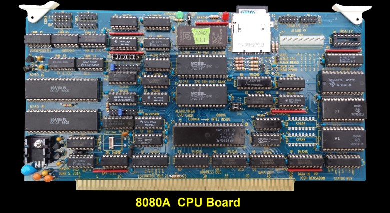
S-100 8080 CPU Board Rev 0.
|
|
Step By Step Building the 8080 CPU Board.
As always, first examine the bare board carefully for scratches or damaged traces, use a magnifying glass if need be. The quality of this board is excellent. However there is always a first time. A broken trace is almost impossible to detect by eye on a completed board. I find it useful to carefully slide a file at 45 degrees along the edges (front & back) of the S100 connector for easier insertion into the bus. Carefully, just one or two strokes.
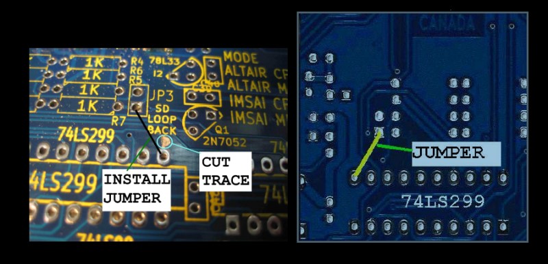
There is a slight error on the board for the SD card interface. Due to propagation issues with the Q1 transistor, it is necessary to direct connect the SD Memory card Data Output directly to the SPI MOSI. The VIH of the 74LS299 is 2V and the Data Output is 3.3V, that will not be enough for a safe logic “1”. This change requires cutting 1 trace and installing 1 jumper wire. Cut the trace on the component side between Pin 11 of IC H4 and the silk screen text “SD LOOP BACK”. Install one jumper wire on the solder side between JP3 and Pin 11. We will omit Q1, R7 and R13 during the assembly below. Here is a picture of the change.
|
|
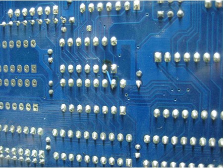
Also pin 15 of the 8T97 (74LS367), IC H7, is left disconnected on the board. We need to install a jumper from IC H7 pin 15 to IC H6 (74LS04) pin 2.
Alternatively, you can hide this jumper under IC H7 by placing it between pins 15 and pin 1 (or by adding a short solder bridge on the back of the board)
Here is a picture:-
|
|
Solder in all the required IC sockets, resistors, resistor arrays, capacitors, jumpers, and the six voltage regulators. Do not add the LED's yet. Be sure you put the resistor array in with the correct orientation of pin 1. Check their values before soldering (they are difficult to remove).
The LM7805C (5.0V, 1.5A) regulator heat sink must as large as possible. Use a mica insulator to insulate the board a little from the heat it generates. Use heat sink compound.
For prototype boards I generally use "double swipe" IC sockets. For a critical board like this I prefer to use "Machine Tooled" IC sockets. However they are more expensive and you have to be particularly careful not to bend the IC pins.
Next insert the two LED's. Before soldering them in place ground pin 9 on the I5 socket and pin 5 of E2 to make sure they light up.
Capacitors C15 to C19 are the 3.3uF Tantalums. These are the capacitors that work on the voltage regulator outputs. They may be somewhat overrated. You can probably use lower values if need be -- as low even as 0.33 uF. The decoupler capacitor under IC-C2 are not critical and are placed there to save space. Use small 0.1uF caps if you have tem.
|
|
Next install all the IC's on the board except:-
The two UARTs (A5 & A6)
Two of the 3 8212's (J5 & J3)
J2 the 74HCT245
and the SD card holder.
Take care to insert the 8080A on to this board upside-down. As we have done for all the other S100 bus CPU bards, we will first bring up the board in a very simple mode where it simply continuously sends a character to the console.
The board only takes a UV EPROM (a 27256 or 27C256), so burn the following code into such an EPROM.
3E 33 D3 01 C3 00 00
I use the Wellon VP-290 to do this. The code is so short you can simply enter the bytes directly within its own programming interface. The board need to be configured as a "master". Unconnected to the front panel (if present) set the following jumpers:-
JP7 1-2
JP6 2-3
JP1 2-3
JP4 1-2
We will place our ROM starting at 0H in memory and utilize the full 64K or RAM space. So jumper the ROM & RAM jumpers as shown here.
|
|
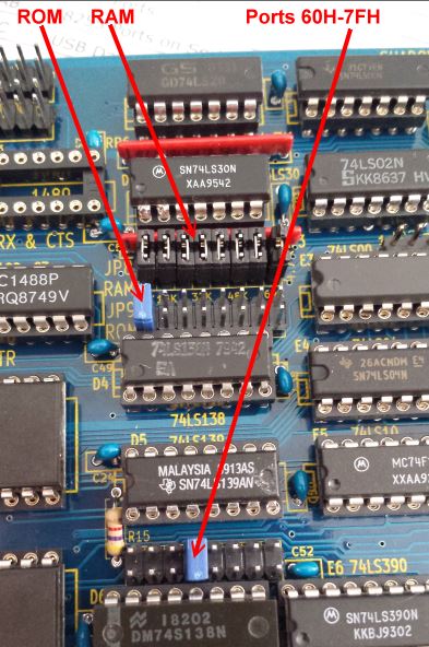
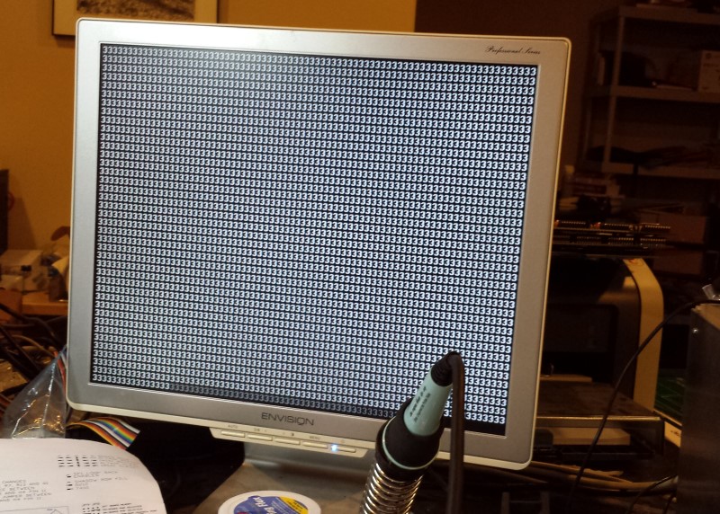
Remember on this board if there is no I/O port jumper, that port address range is available from other S100 bus boards. In my system the console I/O ports are 0H & 1H, so no jumper at the first position of JP10. We will be using the onboard SD card (see below). I have assigned it to the 60H to 7FH ports range. The only other boards I have here that use this range are the Lomas Video board and the old Tarbell cassette board. With the above configuration the board came up fine displaying data on the console as shown here:-
|
|
|
|
|
|
If you do not see the above output it may be because this board does not supply the upper 8 address lines for port I/O. Only address lines A0 to A7 are valid. For many old S100 boards this is all that is decoded anyway. But IEEE-696 boards (and all of our own S100Computes boards), utilize the full 16 bit address range. Fortunately these boards have a jumper to restrict the port range to 8 bits. On our Propeller Console IO board its jumper K5 2-3.
If you get this far you are well on your way to bringing up the board. At this point you can either hook the board up to your Altair/IMSAI front panel or if you have one, insert the SMB. In any case you need to insure that the S100 bus signal MWRT (S100 pin 68) is being generated in your system. On the SMB this is jumper JP11.
Finally this board lets the IEEE-696 Address lines A16 to A23 float. If you are using IEEE-696 RAM/ROM boards these lines need to be grounded if you use them. Since the board has its own 64K of RAM this is probably not a big issue. BTW, our V2-SMB has a circuit to ground these lines (when a 16 bit CPU is not being used).
An 8080 Monitor.
In order to be of any use this board needs to be programmed for the 8080A. We need a monitor program. Monitors tend to be personal things everybody has their own favorites and requirements. Mine is the format/menu of our Z80 "Master" monitor. The problem is it is in Zilog nemonics and in places utilizes the unique special instructions of the Z80. I had to hand recode it into Intel format and expand out the Zilog opcodes into the (longer) 8080A codes. This monitor 8080.ASM can be obtained here. For this board we have one further complication, unlike our Z80 CPU board the is no circuit for a "power on jump" to a specific RAM location (usually F000H). Instead the CPU expects the monitor in ROM to start at 0H. This is a problem for CPM which assumes the availability of low RAM.
Fortunately the board has the capability of switching out the onboard ROM chip giving it the full 64K complement or RAM. Before we do this however we need to relocate the ROM code up to (say) F000H in RAM. Jump to that location and then switch out the
With all the above in place the monitor signs on nicely with all the usual commands such as display RAM, ports, MEM map, substitute RAM, Goto etc.
I have not yet implemented the boot CPM on the IDE of FDC board commands yet. Perhaps somebody else could do that for us all. The code is there its just not yet debugged.
The 8080 Monitor can be downloaded from the link at the bottom of this page.
Notes
Josh has provided a few more recent update notes for builders of this board.
They can be found here.
The links below will contain the most recent schematic of this board.
Note, it may change over time and some IC part or pin numbers may not correlate exactly with the text in the article above.
8080 Board manual (V1.3 8/3/2014)
8080 Board Schematic (V1,0 7/31/2014)
8080 Board Parts List ( 8/3/2014)
8080 Monitor Software (V1,1 7/31/2014)
8080 Monitor & CPM Disk Software (V2.1 12/28/2014)
Rev 1 – Released April 9, 2016 This board is still available. Contact CrustyOMO or post on the Google Groups S100Computers forum if you would like one.
8080 CPU Board Introduction
Other pages describing my S-100 hardware and software.
Please click here to continue...
This page was last modified on 11/01/2018