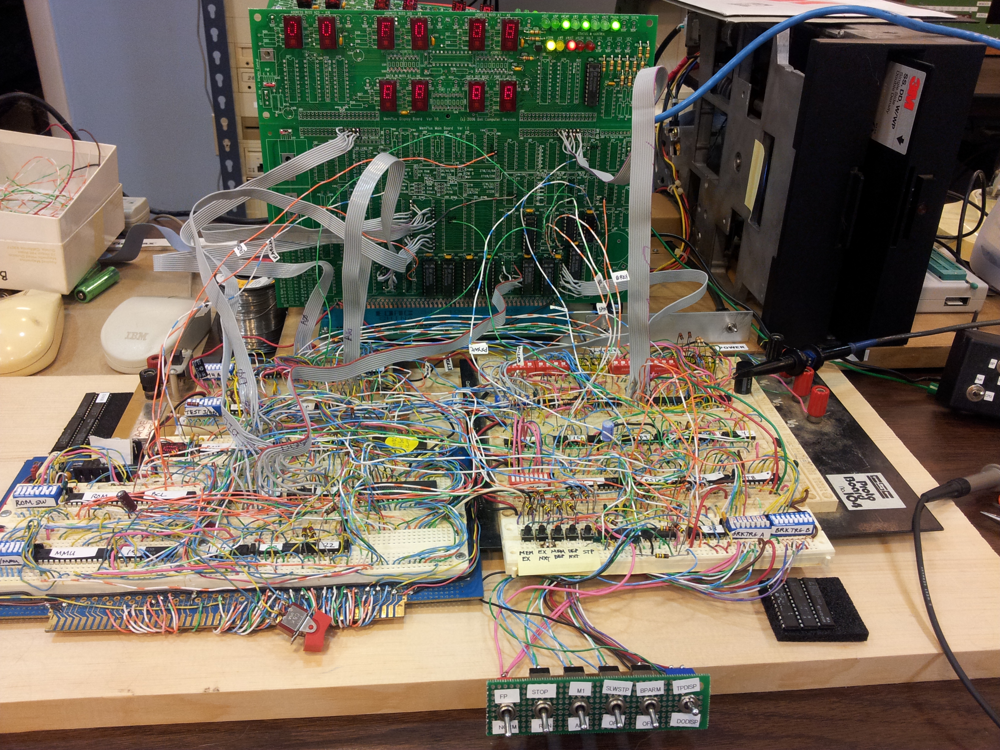
Good evening, S-100 group. I have arrived at nearly the end of the qualification of my Version 2 Mem8Plus board and ran into a rather sticky wicket. I was hoping someone on this group has encountered this issue before and has figured out how to work around it. The problem lies in my hardware breakpoint trigger logic. The design was to permit flexible breakpoint triggering. In the V1 board, I could only break on a memory read of a particular address. V2 is supposed to permit the selection of several options: Memory Read, 16 bit address Memory Read, 24 bit address Memory Read, 16 bit address, with matching data pattern Memory Read, 24 bit address, with matching data pattern M1 Read, 16 bit address M1 Read, 24 bit address M1 Read, 16 bit address, with matching data pattern M1 Read, 24 bit address, with matching data pattern Memory Write, 16 bit address Memory Write, 24 bit address Memory Write, 16 bit address, with matching data pattern Memory Write, 16 bit address, with matching data pattern (There are also similar I/O read and write and Interrupt Acknowledge triggers, but they are irrelevant to this issue.) All Memory Read and M1 Read options work. However, I cannot get the Memory Write options to trigger. Upon very close inspection of the S-100 bus timing, I have discovered that SWO* does not occur until after PSYNC has gone false in T1. In fact, it is not asserting until T2. SWO* would be necessary to tell the breakpoint logic that a memory write operation was beginning, and have the same function as SMEMR and SM1 do in the two sets of read triggers. I traced this back to my CCS 2810 CPU board where I discovered that SWO* is simply buffered WR* from the Z80. Looking at the Z80 technical manual, I see that WR* simply does not occur until T2 of the memory write bus cycle. Presumably, WR* is meant as a memory write strobe, and not the status line that is supposed to be SWO*. XRDY or PRDY (Z80 Wait*)needs to be asserted before the falling edge of the Clock in T2, but with the Z80 WR* line (S-100 SWO*) not going low until the falling edge of the Clock in T2, it cannot possibly de-assert XRDY or PRDY to cause a wait-state, or in my circuit, stop the CPU (infinite wait-states) in that particular bus cycle. Here’s where I’m hoping for some wisdom: Has anyone ever figured out hardware that detects a memory write (but not a memory read) somehow and can activate a wait-state in the current bus cycle? And because this is an S-100 board, I am limited to what is on the bus. E.G. I cannot reach back into the CPU board for anything. The only thought I currently have in mind is to look at SMEMR, SM1, SOUT, SINP and SINTA, and assume that if none are true, then the bus cycle must be a memory write. I don’t like the assume part, but what do you think? Any input would be most appreciated. Bob Bell PS. I attached a snap of what qualification testing is looking like on this board. I hope the attachment goes through. |
Attachment:
20150816_190337.jpg
Description: JPEG image