Thank you.
Please find attached a schematic and board layout pdf.
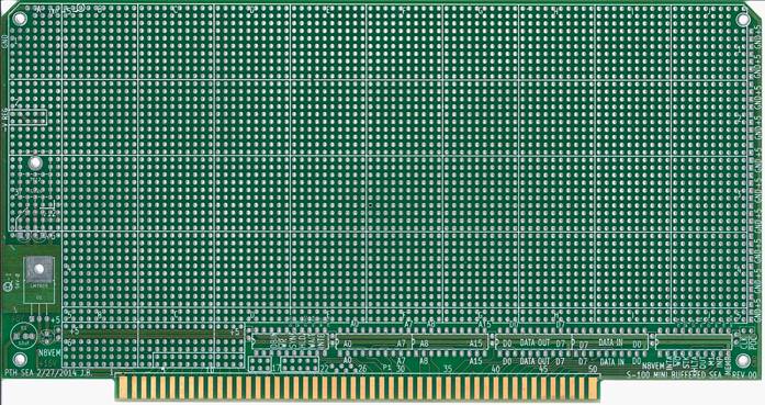
For the short write up, you can say,
S-100 Mini Buffered Prototyping board.
Features:
4042 Holes
+5V Regulator with 74LS245 buffer chips for Address, Data, Status and Control bus.
S-100 connector with gold fingers
Labeled pins on Copper side (where you need it)
+5V and GND power distribution on right edge of card
Fusible Links on the 3 power rails
Optional Power LED
Optional Positive and/or Negative Voltage regulators
Optional holes for Card handle or Card stand-offs
Regards,
Josh
From: mon...@vitasoft.org
To: n8vem...@googlegroups.com
Subject: RE: [N8VEM-S100:4259] Buffered Prototyping Board, Sea-o-PTH
Date: Tue, 17 Jun 2014 21:18:05 -0700
Of course Josh, will do. To be on the safe side could you send me the most current schematic and board layout (pdf’s).
For people that what one in the future, what contact info do you want.
IF, you have time could you write-up a short description and logic etc. for the current design
John
From: n8vem...@googlegroups.com [mailto:n8vem...@googlegroups.com] On Behalf Of Crusty OMO
Sent: Tuesday, June 17, 2014 7:05 PM
To: n8vem...@googlegroups.com
Subject: RE: [N8VEM-S100:4258] Buffered Prototyping Board, Sea-o-PTH
Hi John,
I am hoping you might put my Buffered prototyping board up on your web site.
Also, you can say I have Qty 30 on hand for anyone looking.
Cheers, and Thank you,
Josh Bensadon
--
You received this message because you are subscribed to the Google Groups "N8VEM-S100" group.
To unsubscribe from this group and stop receiving emails from it, send an email to n8vem-s100+...@googlegroups.com.
For more options, visit https://groups.google.com/d/optout.
--
You received this message because you are subscribed to the Google Groups "N8VEM-S100" group.
To unsubscribe from this group and stop receiving emails from it, send an email to n8vem-s100+...@googlegroups.com.
For more options, visit https://groups.google.com/d/optout.