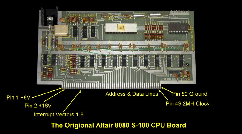
| 1 |
+
8 Volts |
The instantaneous minimum must
be greater than 7 volts. The average maximum must be less than +11
volts and the instantaneous maximum must be less than 25 volts.
The optimum voltage is 8 Volts, but many drop the voltage
to 7.5 volts to lower heating of on-board voltage regulators.
|
| 2 |
+16
Volts |
The instantaneous minimum must
be greater than 14.5 volts. The average maximum must be less than
+21.5 volts and the instantaneous maximum must be less than
35 volts. The optimum voltage is 16 Volts.
|
| 3 |
XRDY |
This
is a signal
that is asserted by a slave to tell the master that it is ready
to complete the current bus cycle. The slave may drive XRDY low
to tell the master that it is not ready to complete the operation.
This will cause the master to wait until RDY goes high again, in
effect extending the current bus cycle.
|
| 4-11 |
VI0*-VI7* |
There are 8 interrupt lines on
the bus. A low on any one will signal to the current CPU that and
interrupt is required. They are typically assigned priorities by
an interrupt controller chip.
|
| 12 |
NMI*
|
A low on this line triggers an
immediate NMI interrupt. This signal need not generate an interrupt
acknowledge and is edge triggered. On a Z80 if INT's are enabled
the CPU will jump immediately to memory location 66H.
|
| 13 |
PWRFAIL*
|
Seldom actually implemented but
triggered to warn the CPU/system on a pending power loss.
|
| 14 |
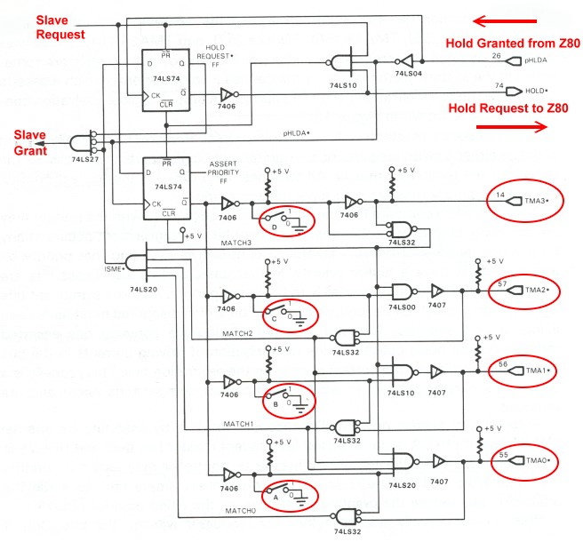
DMA
3* |
One of 4 lines a temporary bus
master sends to the bus Master bus controller signaling that it
wants to have control of the bus. Examples would be an 8086
taking control of the bus from a Z80 bus master or a disk controller
temporarily using the bus for direct memory access.
|
| 15 |
A18
|
|
| 16 |
A16
|
|
| 17 |
A17 |
|
| 18 |
SDSB* |
When this line is low the status
lines sMEMR, sWO, sM1, sINP, sOUT, sHLTA and sXTRQ normally controlled
by the permanent bus master are floated. This allows the temporary
master to control these lines.
|
| 19 |
CDSB*
|
When this line is low the status
lines pSYNC, pSTVAL, pDBIN, pWR and pHLDA normally controlled by
the permanent bus master are floated. This allows the temporary
master to control these lines. Note MWRT is not affected by CDSB.
|
| 20 |
GND |
On old systems this line was controlled
from a front panel to stop or allow writing to RAM. Was almost never
used. Now dedicated to a badly needed ground line in the center
of the board.
|
| 21 |
NDEF
|
This was
the old S-100 Single Step line. It was generated by the front panel.
Single step hardware is useful for debugging but there is no need
for this line. CompuPro (and possibly others) used this line
in some boards (for example their
68000 CPU board) as a Master Clock disable
to allow slaves to come on the bus with a different clock speed.
|
| 22 |
ADSB* |
When this line is low all address
lines (A0-A23) normally controlled by the permanent bus master are
floated. This allows the temporary master to control these lines.
|
| 23 |
DODSB* |
When this line is low the data
output lines (DO0-D07) normally controlled by the permanent bus
master are floated. This allows the temporary master to control
these lines.
|
| 24 |
PHI |
This is the main system clock
for the bus from which all other signals are linked. Both the master
and slave CPU's use this signal. The bus specs are unclear as to
how to implement a faster clock for a slave CPU.
|
| 25 |
pSTVAL*
|
A very important signal. This
strobe indicates the information on the bus for the address and
status lines are valid. Note it is only meaningful when it occurs
with pSYNC.
|
| 26 |
pHLDA |
This is a signal that indicates
that the master has relinquished control of the S-100 Bus to another
master.
|
| 27 |
RFU |
Not currently utilized.
Some people use it as a line for inverse master Clock (24). This
allows boards like the Versafloppy II to work that count on the
old Clock 1 signal on pin 2
|
| 28 |
RFU |
This was the old PINTE line. It
monitored the 8080 to show when INT's are enabled. The signal was
never used
|
| 29 |
A5
|
|
| 30 |
A4 |
|
| 31 |
A3 |
|
| 32 |
A15 |
|
| 33 |
A12 |
|
| 34 |
A9 |
|
| 35 |
D01/DATA
1 |
Data bit 1 out to the bus for
an 8 bit CPU, bidirectional data bit 1 for 16 bit data |
| 36 |
DO0/DATA
0 |
Data bit 2 out to the bus for
an 8 bit CPU, bidirectional data bit 1 for 16 bit data
|
| 37 |
A10 |
|
| 38 |
DO4/DATA
4 |
|
| 39 |
DO5/DATA
5 |
|
| 40 |
DO6/DATA
6 |
|
| 41 |
DI2/DATA
10 |
|
| 42 |
DI3/DATA
11 |
|
| 43 |
DI7/DATA
15 |
|
| 44 |
sM1
|
The name M1 comes from the old
8080 designation for an op-code fetch cycle. This status line signifies
that the master is fetching an instruction from the bus. Depending
on the implementation of a particular master, this line may also
be active during an interrupt acknowledge cycle.
|
| 45 |
sOUT
|
This status line is active when
the master is executing an output cycle and writing data to an I/O
port address.
|
| 46 |
sINP
|
This status line is active when
the master is executing an input cycle and reading data from an
I/O port address.
|
| 47 |
sMEMR
|
This status line is active when
the master is reading from a memory adders. It will go high for
all memory reads including an op-code fetch.
|
| 48 |
sHLTA
|
This status line is active when
the master enters a Halt state. An 8080, 8085, or Z80 microprocessor
enters the Halt state by executing a HALT instruction. An interrupt
request or reset is the only way to get out of a halted state, so
this instruction is usually used to wait for an interrupt to occur.
This instruction may have no equivalent in other processors. In
that case, the processor would never enter the Halt state, and therefore
sHLTA would never become active.
|
| 49 |
CLOCK
|
This is a 2 MHz clock signal that
does not have to be synchronous with the system clock. The
frequency tolerance is + or - 0.5% and the duty cycle is between
40% and 60%. This signal is used as a timing reference for baud
rate generators, real-time clocks, and interval timers.
|
| 50 |
GND |
|
| |
|
|
| |
|
|
| 51 |
+8 Volts |
The instantaneous minimum must
be greater than 7 volts. The average maximum must be less than +11
volts and the instantaneous maximum must be less than 25 volts.
The optimum voltage is 8 Volts, but many drop the voltage
to 7.5 volts to lower heating of on-board voltage regulators.
|
| 52 |
-16 Volts
|
The instantaneous minimum must
be less than -14.5 volts. The average maximum must be grater than
-21.5 volts and the instantaneous maximum must be grater than
-35 volts. The optimum voltage is -16 Volts.
|
| 53 |
GND
|
This was the old S-100 bus Sense
Switch Disable. It was used to active a circuit on the front panel
to input data directly from panel switch.
|
| 54 |
SLAVE
CLR* |
This signal resets all bus slaves
to a known condition. Note that SLAVE CLR* used to be called EXT
CLR*, for external clear. The function is still the same, but the
name was changed to be consistent with the terminology of the standard.
|
| 55 |
DMA
0* |
One of
4 lines a temporary bus master sends to the bus Master bus controller
signaling that it wants to have control of the bus. Examples would
be an 8086 taking control of the bus from a Z80 bus master
or a disk controller temporarily using the bus for direct memory
access. Note: The old Victor Graphic 48K Dynamic RAM boards used
this line to present a short reset signal on the bus to insure the
Z80 could refresh RAM correctly. See
here
|
| 56 |
DMA
1* |
|
| 57 |
DMA
2* |
|
| 58 |
sXTRQ*
|
This is a new status line that
is asserted by the master to request that a 16-bit data transfer
occur during the current bus cycle. If this line is not asserted
(if high) then an 8-bit transfer will be requested by default.
|
| 59 |
A19 |
|
| 60 |
SIXTN* |
This signal
is asserted by a slave device if it is capable of a 16-bit data
transfer. If the master asserts sXTRQ* and SIXTN* is asserted by
the addressed slave within a short period of time, then the
master may proceed with a 16-bit data transfer. If SIXTN* is not
asserted by the slave, then the master should perform the transfer
as two 8-bit transfers. If the master is not capable of performing
the 16-bit transfer as two 8-bit transfers, an error condition will
result immediately, with ERROR* asserted. SIXTN* is a new
S-100 signal not fount on old S-100 boards. However it has been
implemented in a way that makes it compatible with these S-100 boards
- an 8-bit memory board would never
assert SIXTN*.
|
| 61 |
A20 |
|
| 62 |
A21 |
|
| 63 |
A22 |
|
| 64 |
A23 |
|
| 65 |
NDEF |
|
| 66 |
NDEF
|
Some boards
use this line for an output signal from the Z80 refresh signal (for
example
Vector Graphic's Z80 board).
When low, the lower 7 bits of the address lines hold the refresh
address for dynamic RAM boards.
|
| 67 |
PHANTOM*
|
This signal is provided so that
slave devices may exist in the same address space by overlaying
one another. One device (the phantom device) is inactive if PHANTOM*
is inactive and a normal device is active. When PHANTOM* is asserted,
the phantom device becomes active and the normal device becomes
inactive. PHANTOM* may originate anywhere on the bus.
|
| 68 |
MWRT
|
This is
a memory write strobe that is not disabled along with the other
control output bus signals. MWRT is derived from the following equation:
MWRT = pWR-sOUT. In other words, when pWR# is true and sOUT is false,
a memory write cycle is occurring. Note MWRT be generated
by only one device in any system. It may originate on the permanent
master, a front panel, or on any other device that is permanently
in the system. MWRT should be generated by the actual bus signals
pWR# and sOUT. This ensures that any master will be able to write
into memory which uses MWRT.
|
| 69 |
RFU |
|
| 70 |
GND |
This was the old S-100 bus PS
line. I was connected to the front panel LED to indicate that memory
was protected from writing.
|
| 71 |
RFU
|
This was the old S-100 RUN signal.
It was high when the CPU was running and low when the front panel
had stopped the machine. It was never widely used.
|
| 72 |
RDY
|
RDY is a signal that is asserted
by a slave to tell the master that it is ready to complete the
current bus cycle. The slave may drive RDY low to tell the master
that it is not ready to complete the operation. This will cause
the master to wait until RDY goes high again, in effect extending
the current bus cycle.
|
| 73 |
INT* |
This is the general purpose interrupt
request line for the S-100 Bus. It is usually maskable by a software
instruction. When asserted by a slave, assuming the master has not
masked interrupts, after completing the current cycle the master
will enter an interrupt acknowledge cycle or cycles. Usually the
interrupting device will send some kind of information to the master
during the interrupt acknowledge cycle. Note that INT* should
be asserted as a level, meaning that INT* should remain low until
the interrupting device has been serviced.
|
| 74 |
HOLD*
|
This signal is asserted
by a temporary master to request that the permanent master relinquish
the bus to the temporary master. The temporary master should continue
to assert HOLD# until it determines that it is either done with
the bus or will not be granted access. HOLD* may be masked at any
time by the permanent master.
|
| 75 |
RESET*
|
This signal resets all bus masters
to a known condition. Any bus slave that needs to start in a known
condition relative to the master may also be reset by RESET*. RESET*
is often connected to a pushbutton switch located somewhere on the
machine. Note some of the early dynamic RAM boards (that did
not have their own onboard refresh controller and relies on the
Z80 refresh signal) suffered data loss if the refresh pulse was
too long.
|
| 76 |
pSYNC
|
This is a strobe that indicates
the start of every bus cycle. It becomes active very near the beginning
of every bus cycle, and remains active for approximately one cycle
of the bus clock (pin 24).
|
| 77 |
pWR*
|
This signal is the generalized
write strobe for the S-100 Bus. It is asserted
for memory and I/O write cycles. It is used by the slave device
to tell when the data output bus contains valid data.
|
| 78 |
pDBIN
|
This signal is the generalized
read strobe for the S-100 Bus. It is asserted for memory read, I/O
read, and interrupt acknowledge cycles. It is used by a slave device
to turn on its data bus drivers so that the data to be read
is gated onto the bus at the proper time. The master should sample
the data near the end of this read strobe.
|
| 79 |
A0 |
|
| 80 |
A1 |
|
| 81 |
A2 |
|
| 82 |
A6 |
|
| 83 |
A7 |
|
| 84 |
A8 |
|
| 85 |
A13 |
|
| 86 |
A14 |
|
| 87 |
A11 |
|
| 88 |
DO2/DATA
2 |
|
| 89 |
DO3/DATA
3 |
|
| 90 |
DO7/DATA
7 |
|
| 91 |
DI4/DATA
4 |
|
| 92 |
DI5/DATA
13 |
|
| 93 |
DI6/DATA
14 |
|
| 94 |
DI1/DATA
9 |
|
| 95 |
DI0/DATA
8 |
|
| 96 |
sINTA |
This status line is active when
the master is responding to an interrupt request and expects the
interrupting device or interrupt controller to place data on the
Dl bus during this cycle.
|
| 97 |
sWO*
|
This status line is active when
the master is currently executing a memory write
or an output write cycle.
|
| 98 |
ERROR* |
This is a generalized error signal
line that can be used to inform the master that some kind of error
has occurred. This can be a memory parity error, an attempt to write
into a protected memory location, an attempt to perform a 16-bit
transfer to an 8-bit device, etc. This feature was rarely
implemented on the bus. On the Altair S-100 bus, this line was used
to monitor the 8080 Stack line status. No other CPU have such a
signal. Was never used. SD Systems on early boards, used this pin
as a "debug" line. When forced low their CPU board forced address
lines A14 & A15 low allowing their monitor program to go to address
C000H. Some even older boards used pin 98 as a dynamic RAM
refresh signal.
|
| 99 |
POC* |
This signal
must start out low when the system powers up, and remain low for
at least 10 milliseconds after power is stable. POC* must be active
only at power-on. POC* must also assert RESET* and SLAVE CLR*.
|
| 100 |
GND |
Ground |