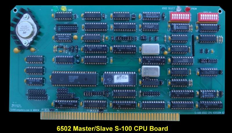
| Jumper |
Function |
| JP4,JP5,JP6,JP7,JP19 |
Used only if the board is
to act as a bus master. Generates Power On reset etc. |
| JP8 |
Use only if no other board
on the bus pulls up the S-100 HOLD signal |
| JP9 |
Use only if no other board
on the bus pulls up the S-100 HLDA signal |
| K2, K3 |
Normally 2-3. Use 1-2 if
board is a bus master. |
| K1 |
Normally 1-2 if slave. 2-3
if master. Controls when 6502 Active LED (D4) lights up |
| K5 |
Normally 1-2. |
| K4 |
Normally 2-3.
Determines how and what S-100 bus interrupts will triggered
the CPU |
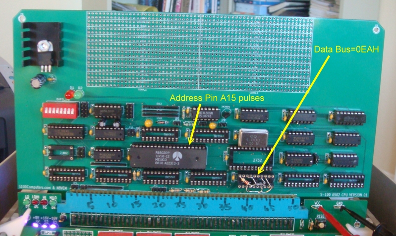
| P11 |
Use only if no other board
generates the S-100 2MHz clock signal when the 6502 is active |
| JP11 |
Use only if no other board
generates the S-100 MWRT signal when the 6502 is active |
| SW1 |
Sets number
of wait states for onboard EEPROM (0-8). I use 0 wait states, so all
switches open for 4MHz CPU |
| SW2 |
Sets number
of wait states for bus I/O and INTA cycles (0-8).
I use 0 wait states, so all
switches open for 4MHz CPU |
| P7 |
Normally set 2-4. Use 1-3
if board is bus master |
| JP12, P13 |
Use only if no other board
on the bus pulls up these signals when board is active |
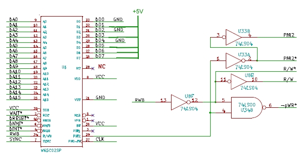
| JP14,P31,JP15 |
These pins must be
carefully selected for different EEPROM and EPROM types. (For
28C64:- Close JP14, P31-2-3, JP15 Open) |
| P30 |
Normally 1-2, This
selects the port bit that activates the CPU in slave mode. If 0,
board is activated. |
| P2 & P3 |
This selects where the
onboard EEPROMS will reside in the CPU's 64K address space |
| P10 |
This selects the S-100 I/O
port that is used to activate the CPU in slave mode. |
| P34, P35, P36 |
These jumpers are to pull
up the S-100 bus Interrupt and DMA lines IF
no other board on the bus pulls them high. Normally they are
not jumper (they are pulled up by the Z80 master CPU). It is
essential multiple boards do not pull them high. |
| P5 |
Determines how
master/slave switchover is accomplished. 1-2 the onboard port, else
another board lowers a DMA line |
|
K7 |
Normally
2-3. Fine tunes when the S-100 bus sSTVAL* is sent |
| JP1,JP2, JP3 |
These are jumpers that
allow you to utilize extra board ground lines as defined in the
IEEE-696 specs. Nor required, do not use with older S-100 systems |